1. Introduction
With the rapid and continuous development of nano-technology, the surface structures in the nanomanufacturing industry are becoming increasingly complex, leading to ever-increasing demands for a large measurement range with high precision in structured surface metrology [
1,
2,
3]. The high precision measurement of critical parameters plays an important role in nanomanufacturing technology. Parameters such as step height, line spacing, tilt angle, surface roughness, etc., are critical for the final performance control of nano-devices like integrated circuits. Atomic force microscope (AFM) has gained attention in micro- and nano-structured surface metrology due to its high resolution, three-dimensional imaging, and nano-scale precision [
4,
5,
6]. Conventional AFM uses piezoelectric ceramics (PZT) to drive the movement of its measurement probe, having the advantage of nano-scale accuracy, but PZT generally possesses a small stroke that makes it difficult to achieve large-scale scanning measurements [
7,
8]. In addition, in order to ensure the accuracy and traceability of the measurement results, the conventional AFM needs to be calibrated regularly [
9,
10]. Generally, standard artifacts are used to calibrate their horizontal and vertical characteristics and
X-
Y orthogonality. However, the calibration process is complex and difficult to achieve full-range calibration. Meanwhile, the standard artifact will also introduce a new source of uncertainty to the measurement system.
In order to overcome the defects of traditional AFM, Gonda et al. [
11,
12,
13,
14] developed a real-time, interferometrically measuring atomic force microscope for direct calibration of standards; the measuring range of the system is 17.5 μm × 17.5 μm × 2.5 μm. In addition, Misumi et al. used this system to research probe tip diameter evaluation and profile surface roughness measurement. Furthermore, Haycocks et al. [
15] used a commercial AFM head and a flexure stage to build a metrological AFM system. The system has a range of 100 μm × 100 μm × 5 μm and was used for measuring step and pitch standards. Dai et al. [
16,
17,
18] constructed a metrological largerange atomic force microscope based on the nano-measuring machine. The system can measure samples up to 25 mm × 25 mm × 5 mm and realize high scan speeds of up to 1000 μm/s. Wei et al. [
19] designed and built a metrological AFM measurement system using four laser interferometers for characterizing nanostructures. The system can realize a displacement range of 50 mm × 50 mm by mounting a nano-stage on an air-bearing two-dimensional displacement platform, but the nano-stage is constructed by PZT, which confronts the problems of nonlinearity and hysteresis. Wang et al. [
10,
20] used a metrological AFM system based on the Danish Micro Engineering A/S atomic force scanning head and nano-measuring machine to measure the step structure. Xiao et al. [
21] built a probe-scanning AFM system for wafer measurement by adopting a macro–micro combination drive mode in the
X-
Y plane. It can realize the detection of 12-inch wafers with a resolution of 0.2 μm, but its scanning range is limited to 40 μm.
Herein, we propose a measurement system with high precision and a large measurement range based on Nanosurf NaniteAFM and the NMM-1 nano-measuring machine [
22,
23]. A mechanical structure with a large movement scale and traceable positioning capability expands the measurement range from 110 μm × 110 μm × 20 μm to 25 mm × 25 mm × 5 mm. Furthermore, a signal amplifier with low noise and a high common mode rejection ratio decreases the noise level of the measurement system to 2 nm.
Section 2 introduces the principle of the measurement system in detail.
Section 3 demonstrates the performance of the system through three experiments, respectively, on the measurement and characterization of an ultrahigh step, an atomic deposition grating, and a tool tip structure. Finally, a discussion and a conclusion are made in
Section 4 and
Section 5, respectively.
2. Principle of the Measurement System
The metrological AFM measurement system mainly includes a positioning system, an atomic force scanning system, a signal amplifier (AMP), a computing system, an AFM controller, and an NMM-1 controller. The positioning and scanning systems are presented in detail in
Section 2.1 and
Section 2.2, respectively.
Section 2.3 introduces the integration of the whole metrological AFM measurement system as well as some important components like AMP and the controllers, along with the signal processing method. Finally,
Section 2.4 introduces the calibration of the metrological AFM measurement system, which is vital to the measurement precision and accuracy.
2.1. High Precision Positioning System
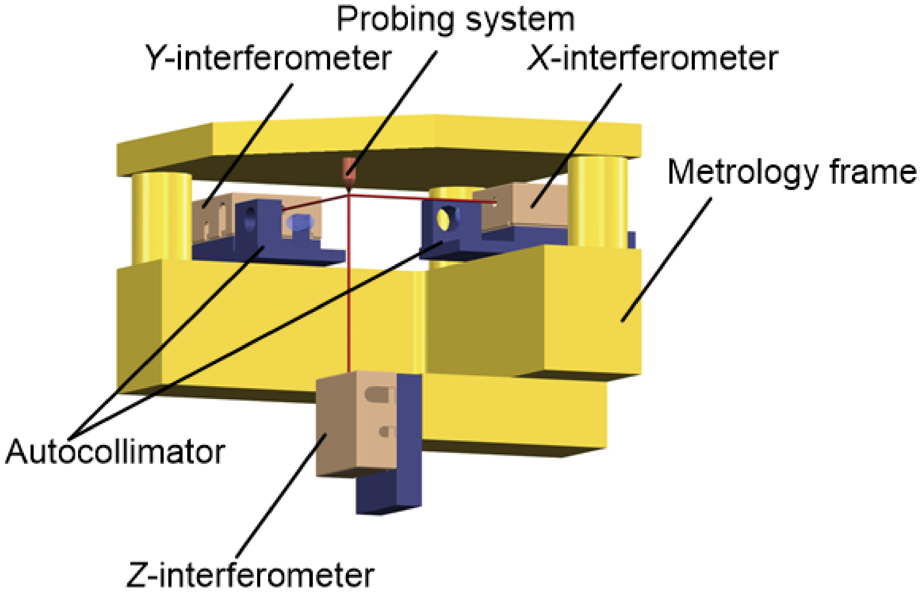
The metrological structure of the positioning system is shown in
Figure 1, consisting mainly of a probing system, autocollimator,
X-interferometer,
Y-interferometer,
Z-interferometer, metrology frame, etc. The
X- and
Y-axis of the positioning platform are driven by a direct current linear motor, the
Z-axis is driven by four groups of voice coil motors, and all the axes use three miniaturized plane mirror laser interferometers as displacement feedback. The SP-DIS series laser interferometers use the frequency-stabilized He-Ne laser and can achieve a resolution of 20 pm. The driven system and metering system are designed separately to ensure positioning accuracy. In order to achieve a zero Abbe error design, the three-axis laser interferometers of the positioning system are arranged in an orthogonal manner, the optical pathed intersect at a point, and two autocollimators are used to correct the pitch, yaw and roll of the moving platform [
24,
25,
26,
27]. Due to the above measures and some unique control algorithms, the positioning system can achieve a resolution of 0.1 nm in all three-axis directions within 25 mm × 25 mm × 5 mm.
The three-axis laser interferometers share a frequency-stabilized laser light source through the beam splitter, and the laser is calibrated by an authoritative metrology agency to ensure the traceability of the measurement results. The calibrated laser wavelength is 632.99124 nm, and the frequency is 4.7361233 × 10⁸ MHz. The software and hardware interface of the platform adopts an open design, which is convenient for the integration and secondary development of different types of probes. The platform controller can receive eight analog signals with a voltage range of ±10 V as the feedback input of the control system, and the input bandwidth is 6.25 kHz. The integrated probe output voltage range and bandwidth shall be within the above range.
2.2. Atomic Force Scanning System
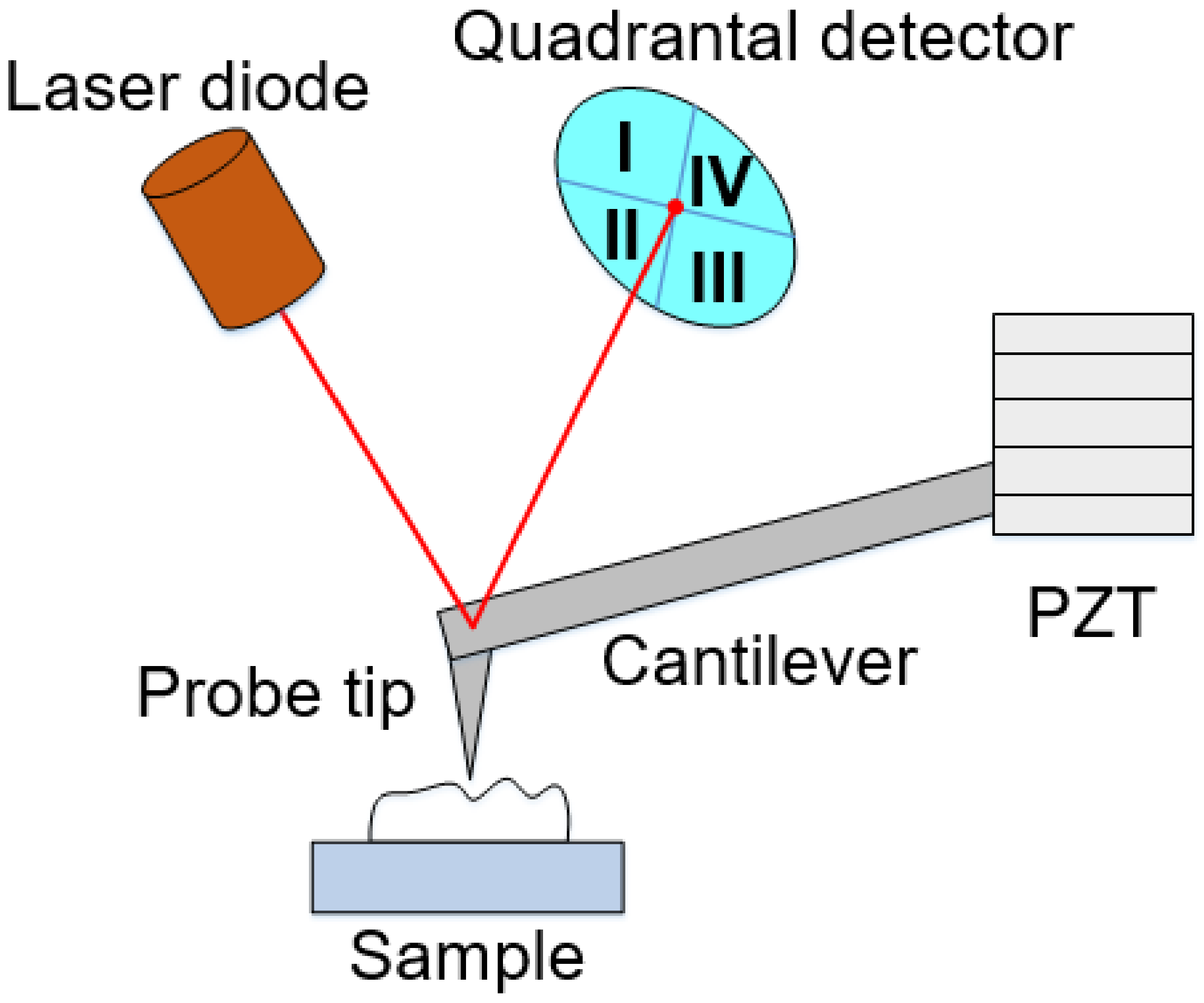
The principle of the scanning head is shown in
Figure 2. It mainly includes the laser diode, the quadrantal detector, and the scanning head. The scanning head possesses a piezoelectric scanner combining a cantilever and a probe tip. Its scanning range is 110 μm × 110 μm × 20 μm, and the linear errors in
X- and
Y-directions are less than 0.6%, respectively. The typical noise level of the
Z-axis is 0.35 nm in static force mode and 0.09 nm in dynamic force mode. The probe’s overall transverse and longitudinal resolution is better than 1 nm. The force between the probe tip and the atoms on the sample surface is realized by the deformation of the detection cantilever.
To facilitate observation and operation, the proposed atomic force scanning system is equipped with lighting LED, overhead, and tilt observation cameras. The overhead camera is used to find the feature area to be measured, and the tilt observation camera is used to observe the proximity of the probe to the sample surface and display the scanning status in real time during scanning. The output signal range of the probe controller is ±1 V. The output signal bandwidth is 740 Hz in the static force mode and 6 kHz in the dynamic force mode, meeting the requirements of the positioning system for the feedback signal range. The scanning system has a compact structure and can be mechanically integrated conveniently.
2.3. System Integration
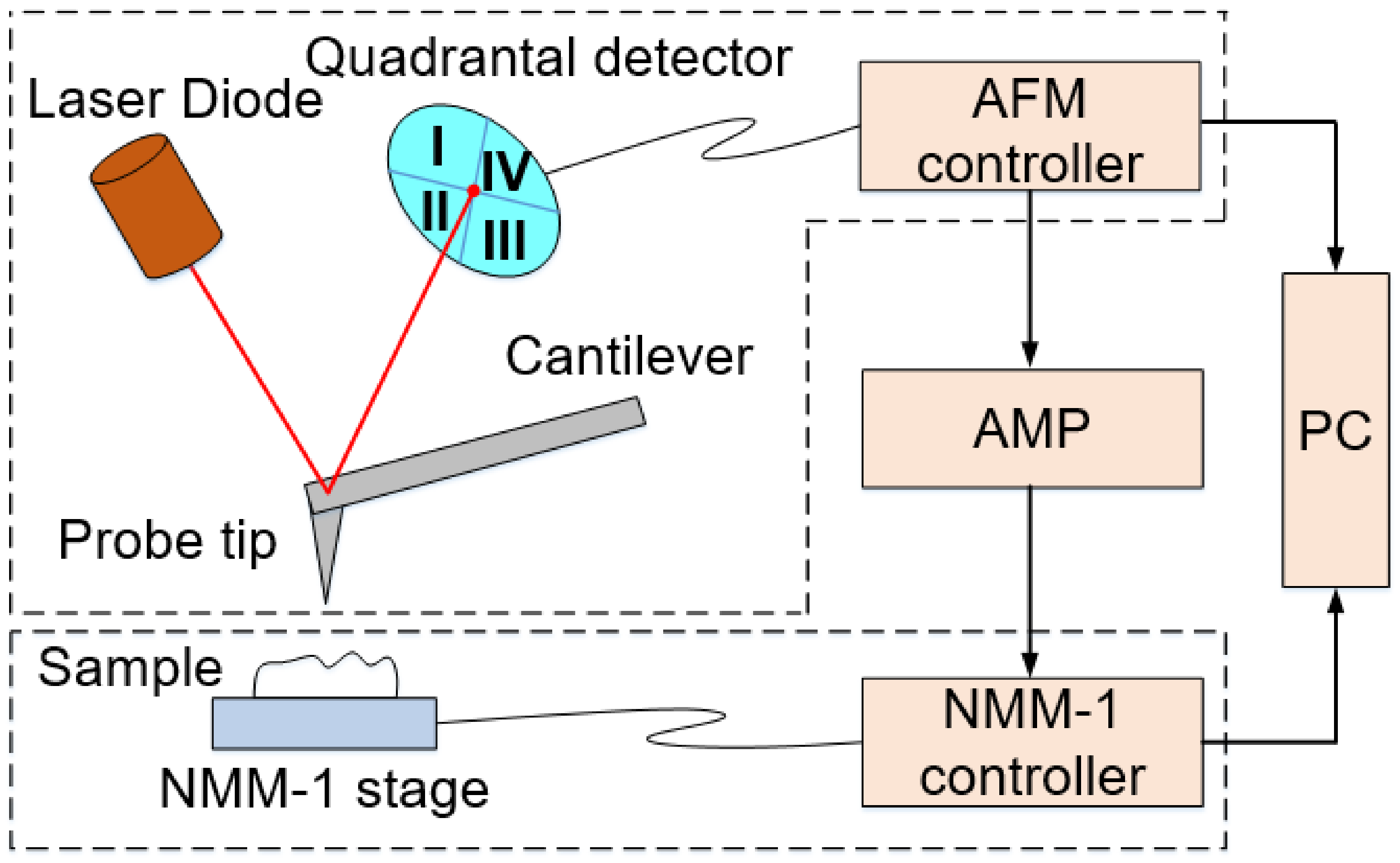
The metrological AFM measurement system mainly includes a positioning system, atomic force scanning system, AMP, computing system, AFM controller, NMM-1 controller, etc., as shown in
Figure 3. In the metrological AFM measurement system, the piezoelectric scanner attached to the scanning system does not work, and the driving and data recording of the sample during measurement is realized by the positioning system. The probe provides feedback signals to the controller of the positioning system. A/D-converters of the digital signal processor (DSP) unit sample the analog signal and calculate the length value
AZ with the following cubic equation:
where
AZ is the displacement-dependent length value calculated from the cubic function,
adc is the value of the A/D-converter, and
k1,
k2,
k3, and
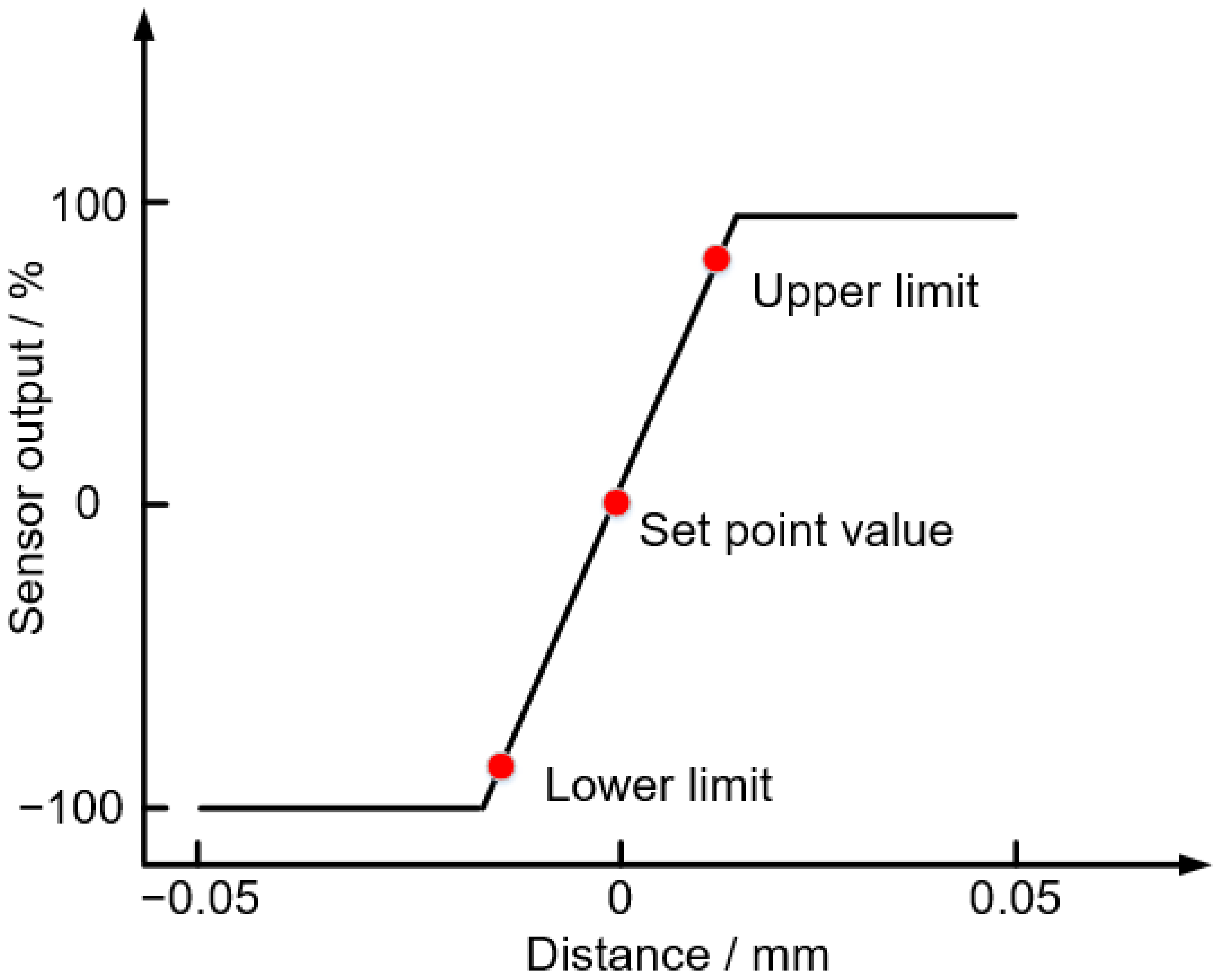
k4 are the coefficients. The coefficients are determined by the characteristic curves of the AFM system. The characteristic curves are obtained by taking a simple set of calibration procedures. The output characteristic curves of the AFM system are recorded by moving the NMM-1 stage up and down ten times. A typical characteristic curve of the AFM system is similar to
Figure 4. During an automatic measuring procedure, the position control is always switched to the set point value when the distance exceeds the upper or lower limit of the sensor output. The
Z value is calculated by the following equation:
where
LZ is the
Z-axis laser interferometer value.
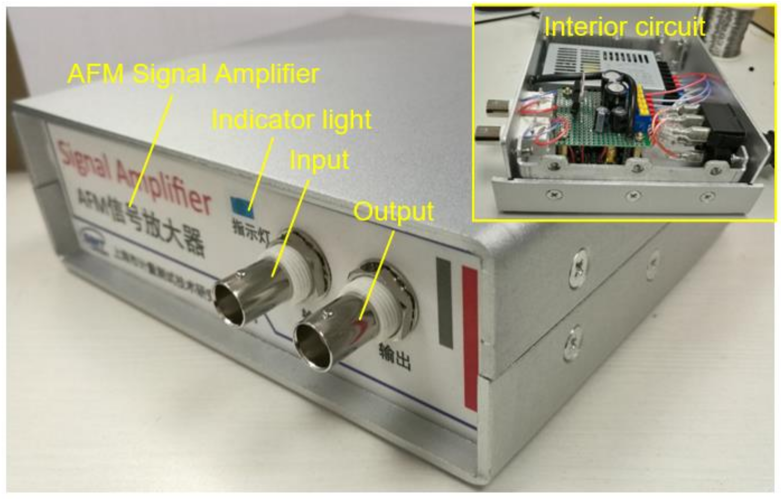
The range of feedback signal output by the AFM controller is ±1 V, but the range of feedback signal received by the NMM-1 controller is ±10 V. To improve the signal-to-noise ratio of the feedback signal and to reduce the noise impact of the NMM-1 controller, it is necessary to amplify the feedback signal output by the AFM controller. An amplifier is designed based on an OP07 high precision operational amplifier with low noise and a high common mode rejection ratio. A series of anti-interference measures are taken to suppress power supply ripple and external noise interference. The circuit uses magnetic ferrite beads to block the interference source to filter the highfrequency noise and peak interference in the signal. The beads distribute at the input and output end of the amplifier circuit. In addition, the root mean square (RMS) noise before and after blocking is 3.875 mV and 1.075 mV, separately. The noise is greatly attenuated. The circuit is encapsulated with a metal shell, and the amplifier panel and signal connection interface are designed, as shown in
Figure 5. The signal is transmitted with a shielded cable of the BNC interface to reduce external electromagnetic interference.
The RMS noise of the signal from the AFM controller and after the low noise amplifier is also tested. The values are 0.313 mV and 1.470 mV, respectively. The noise from the AFM controller is inherent in the AFM electronic system. Although the noise will be amplified synchronously with the measurement signal after passing through the amplifier, it is not dependent on the measurement signal range. Moreover, it can be seen that the noise reduction measures inside the amplifier have a certain effect on reducing the amplified noise of the AFM controller.
2.4. System Calibration
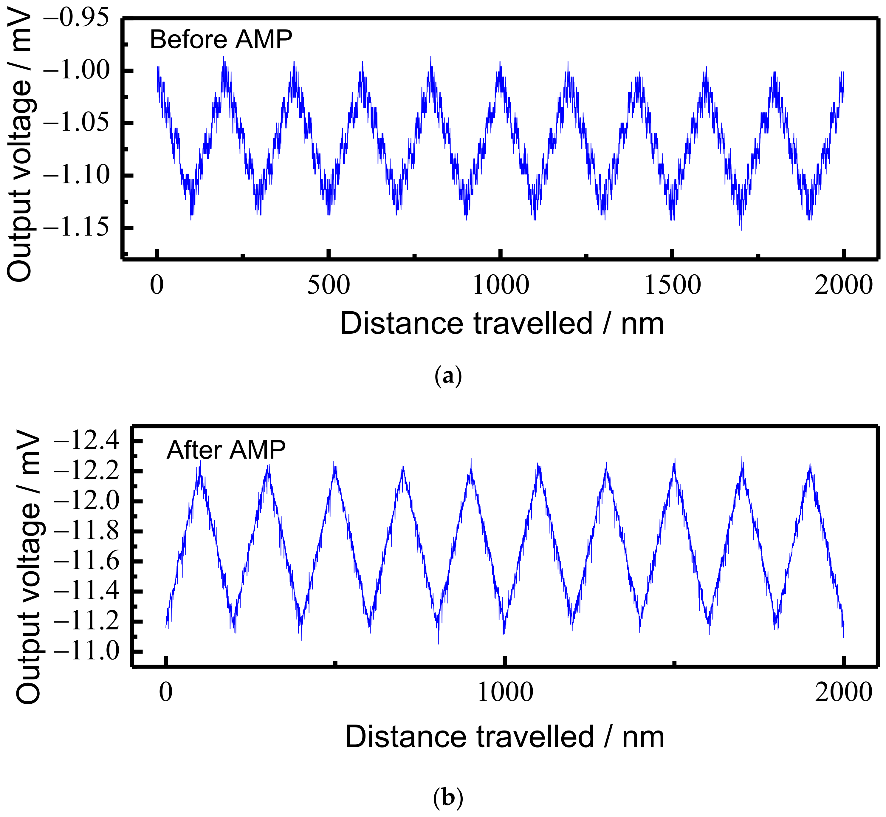
The output signal of the scanning head and the system noise are calibrated and analyzed respectively before measurement. First, make the probe approach the surface of the measurand, then perform the reciprocating movement in the preset interval of NMM-1, record the AFM output signal, and store the calibration results. In order to verify the function of AMP in the whole measurement system, the scanning system is calibrated before and after installing the AMP. The calibration interval is set to 100 nm. The calibration results are shown in
Figure 6. The horizontal axis in the figure is the distance traveled by reciprocating motion, while the vertical axis is the voltage recorded by the A/D converter.
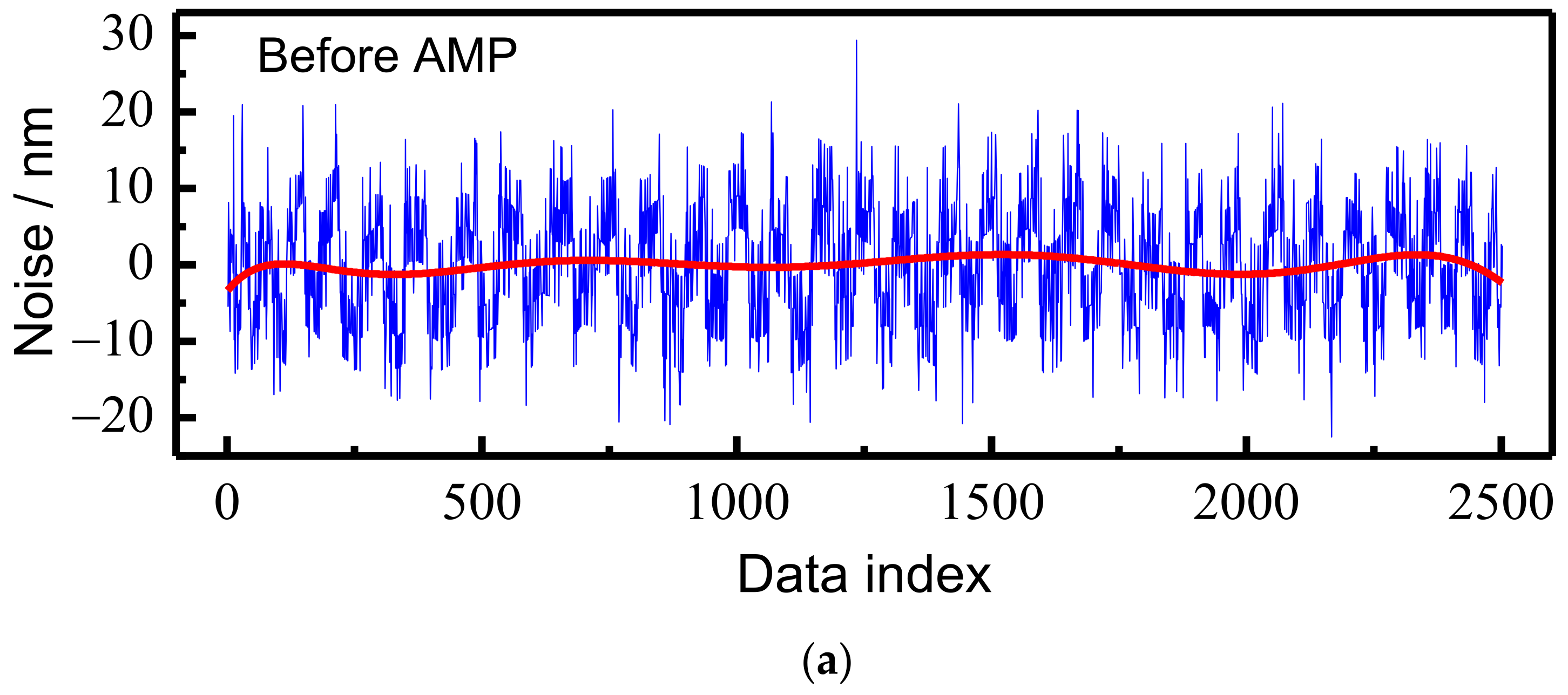
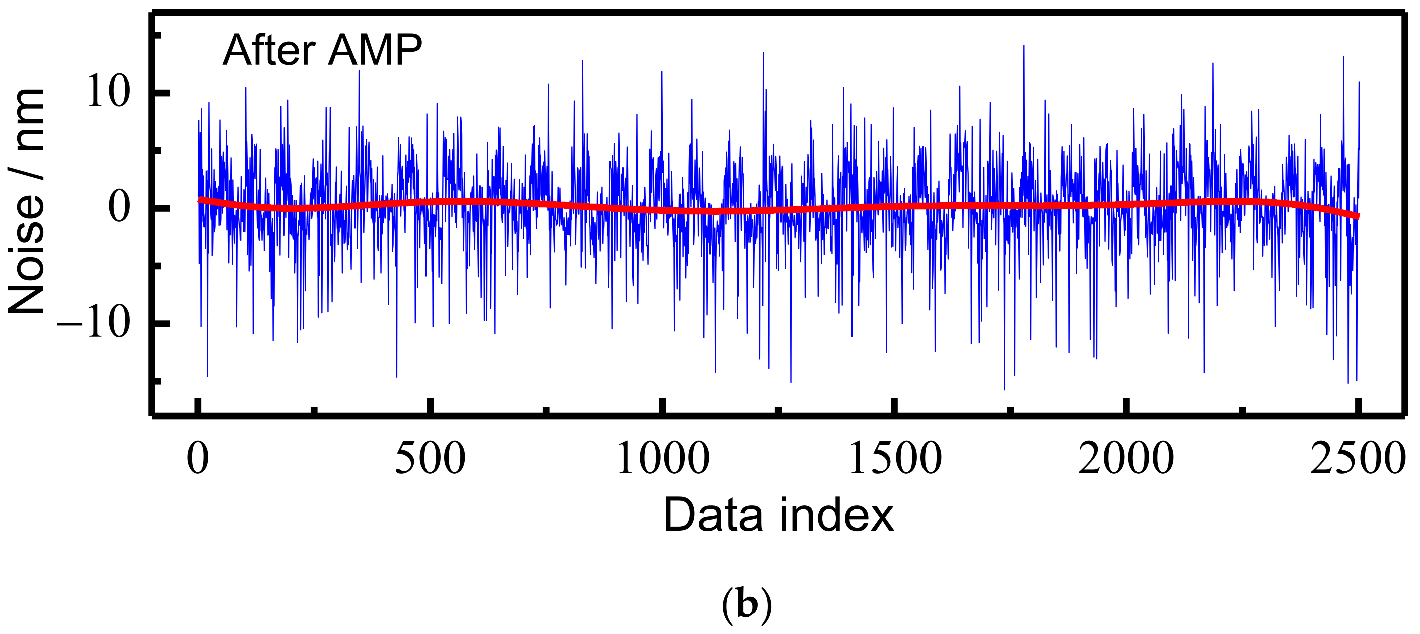
The sources of the noise of the measurement system include not only the AFM controller, the AMP, and the NMM-1 controller but also environmental vibration, temperature change, etc. To characterize the noise level of the whole measurement system, the noise level of the measurement system before and after amplification is tested, and the results are shown in
Figure 7, which indicates that the range of the noise decreases from [−20, 30] to [−10, 10]. The noise peak values before and after amplification are 40 nm and 20 nm, respectively. The noise curve is polynomial fitted using the least squares algorithm, and the fitted noise curve is shown by the red line in
Figure 7. The noise levels before and after amplification are less than 5 nm and 2 nm, respectively. The results demonstrate that our proposed method for noise blocking is valid.
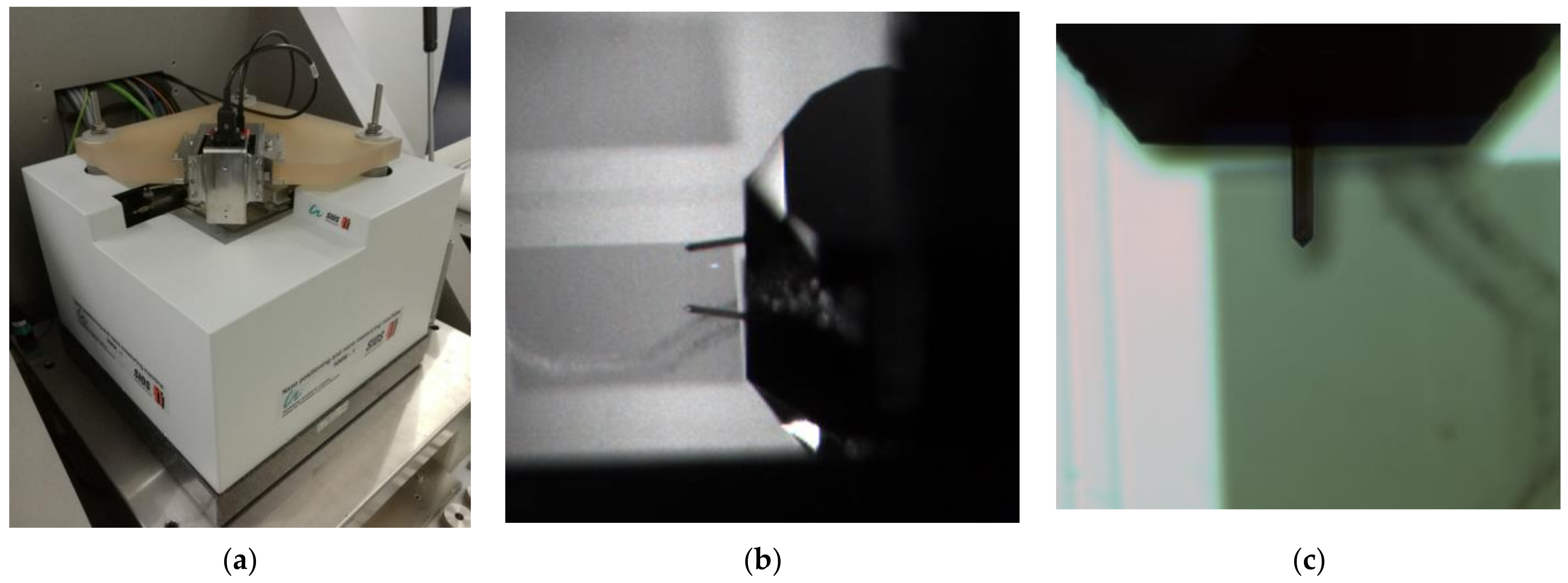
The scanning and positioning systems are integrated using clamping, as shown in
Figure 8a. The clamping is manufactured by invar steel to ensure stiffness and reduce the influence of ambient temperature variation because the invar material has high stiffness and a low temperature coefficient. The electrical connection is also realized with a signal amplifier, as described above. After integration, the measurement range of AFM expanded from the original 110 μm × 110 μm × 20 μm to 25 mm × 25 mm × 5 mm, and the measurement result is traceable. In addition, the AFM probe comes with two cameras for auxiliary observation during measurement. The cameras provide top and side views, as shown in
Figure 8b,c.
3. Experimental Studies
Three-dimensional topography measurement of microstructures is a significant test content for studying micro-processing technology and micro size characteristics. With the progress of processing technology and level, device structures are becoming increasingly complex, and whose accuracy of local parameters on a single device must be higher and higher. However, it is difficult for conventional AFM and optical instruments to have the characteristics of a large range and high accuracy. In this paper, taking the measurement of ultrahigh step, atomic deposition grating, and cutting tool as examples, the application of the ultra-large range metrological atomic force microscope in measuring such structures is described. All experiments are conducted in a thousand-grade clean room ten meters underground. The measurement system is placed on an air-floating vibration isolation platform with an isolation chamber to keep the temperature and humidity stable. The temperature of the environment during measurement is controlled in the range of 20 ± 0.5 °C, and the humidity is 50 ± 5%.
3.1. High Step Measurement
Step structures widely exist in semiconductor and ultraprecision machining. For steps with low height (less than 2 μm), traditional optics or SPM methods can accurately characterize the step height. For ultrahigh steps with a height of more than 2 μm, or even up to the millimeter level, measuring such structures often requires high requirements for the probe and platform, which is difficult to achieve with traditional SPMs. In this paper, the target instrument is used to measure the height of a 4.5 μm step standard sample. The step adopts the SHS-4.5QC standard template of VLSI, and the calibration value of this template is (4.500 ± 0.058) μm.
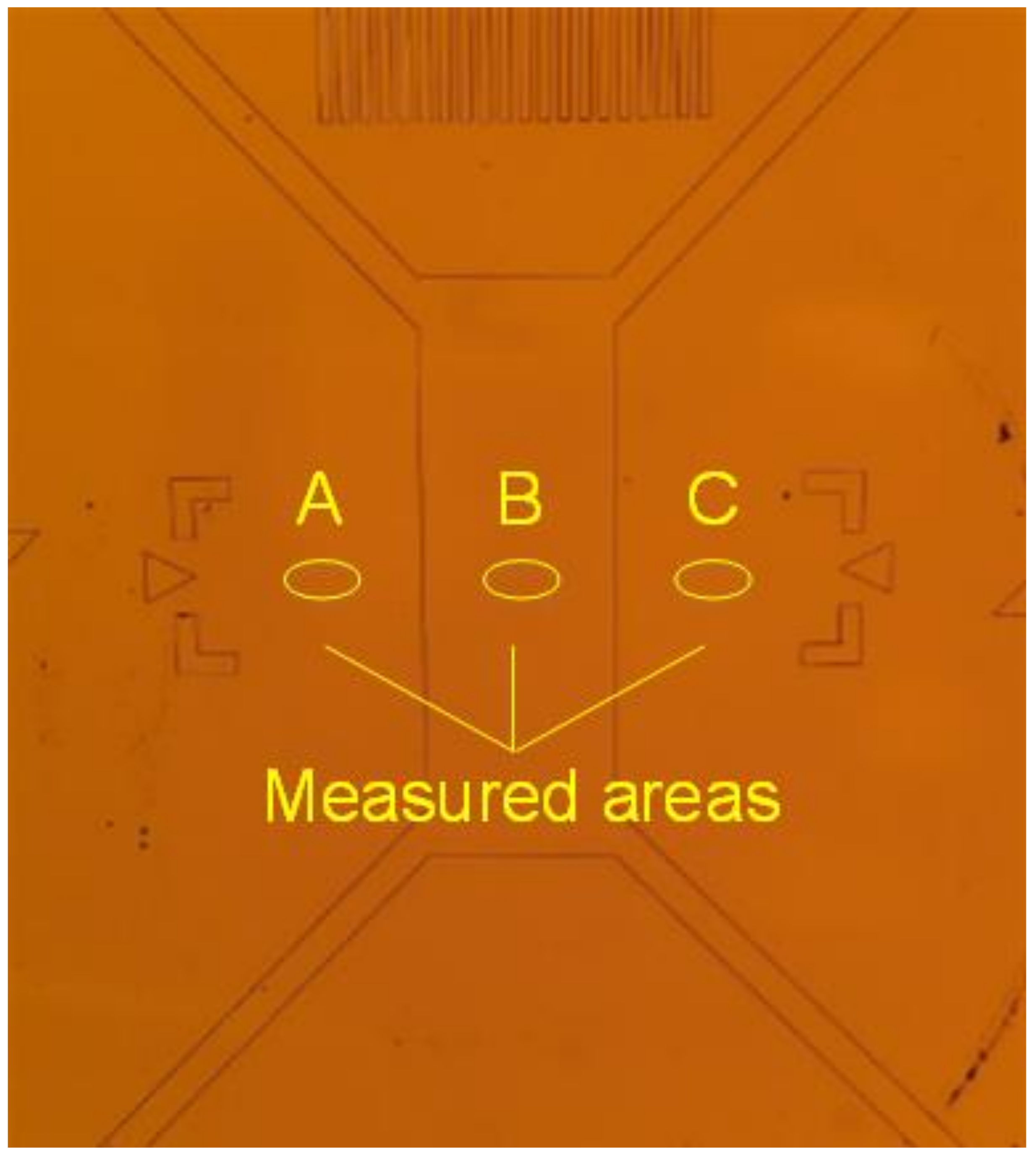
Figure 9 shows the step structure under a BX51 microscope from Olympus with a magnification time of 20.
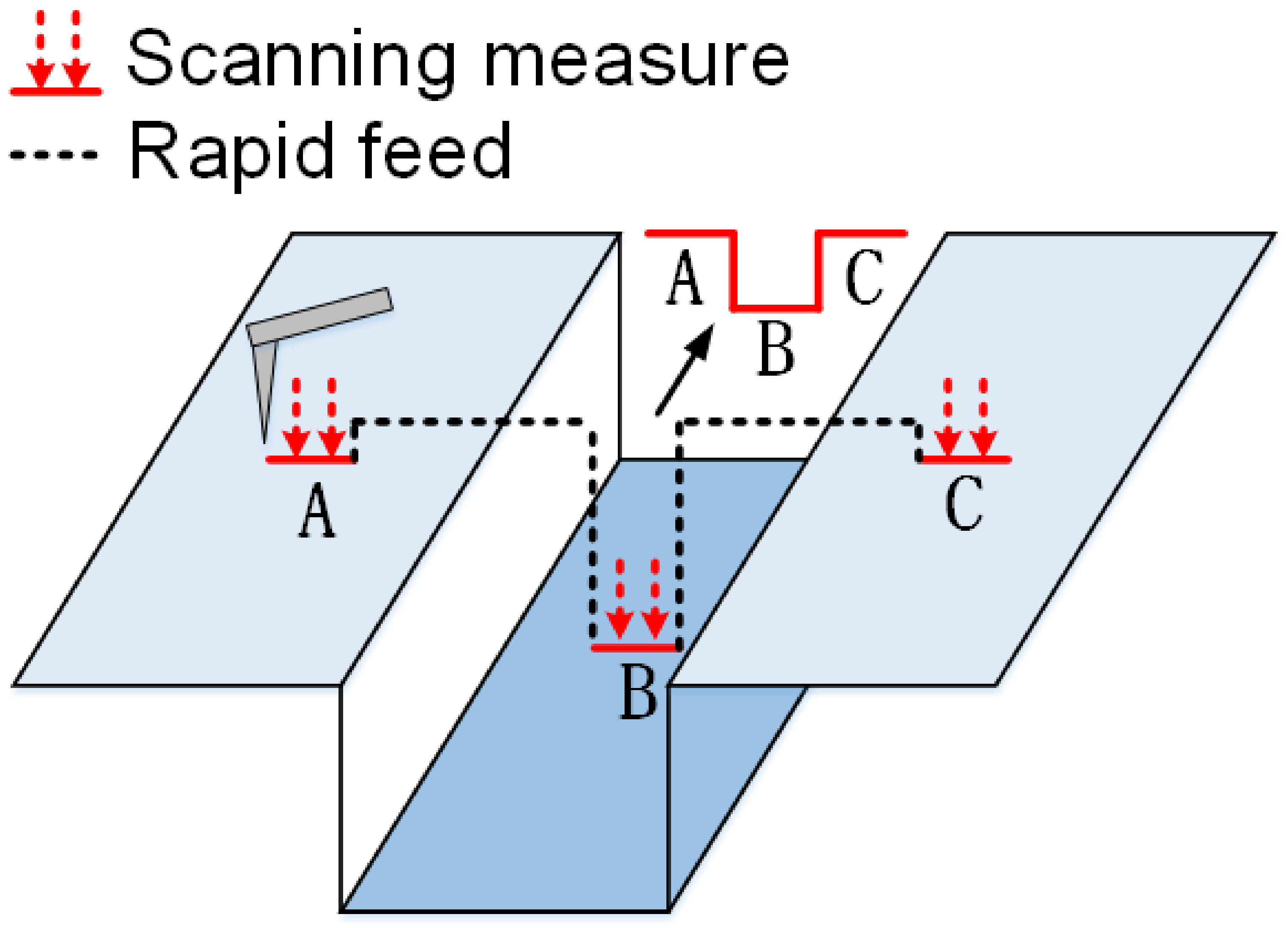
Due to the large size of the measured step, it is difficult to measure the complete structure. Therefore, the method of sectional measurement in this paper is used to measure the A, B, and C positions of the step structure, as shown in
Figure 10. Then, the measurement results are spliced and evaluated using the method defined in ISO5436-1.
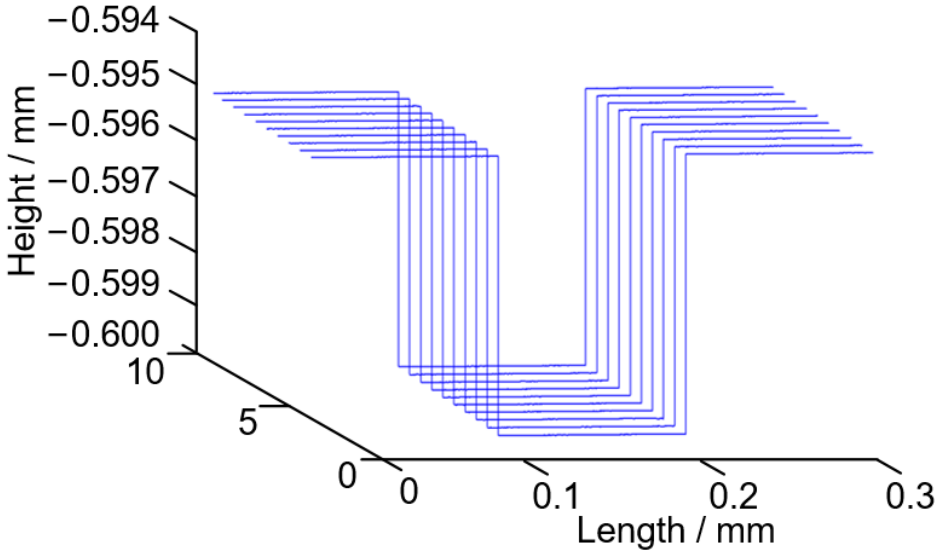
During the measurement, the scanning length of A, B, and C segments is 100 μm, the sampling interval is 0.02 μm, the mean value of ten repeated measurements is 4.553 μm, and the standard deviation is 18 nm. The contour line after splicing is shown in
Figure 11.
Affected by the measuring environment, the instrument noise, and the measurement sample, there is a certain deviation between the measured result and the true value. According to the source of measurement error, the uncertainty mainly consists of the following components: (1) us, the uncertainty introduced by repeatability. (2) uλ, uncertainty introduced by laser interferometer wavelength. (3) uz, the uncertainty introduced by axial motion error of laser interferometer. (4) up, the uncertainty introduced by the AFM system. (5) ut, the uncertainty introduced by temperature change. Based on historical data and experiments, the value of the uncertainty component is as follows.
The combined standard uncertainty can be described as
where
u is the combined standard uncertainty; according to Equation (3) and
Table 1, the combined standard uncertainty of 18.12 nm can be calculated. In addition, the expanded uncertainty is 36.24 nm (
k = 2). Therefore, the measurement result of the step standard is (4.553 ± 0.036) μm (
k = 2).
3.2. Atomic Deposition Grating Measurement
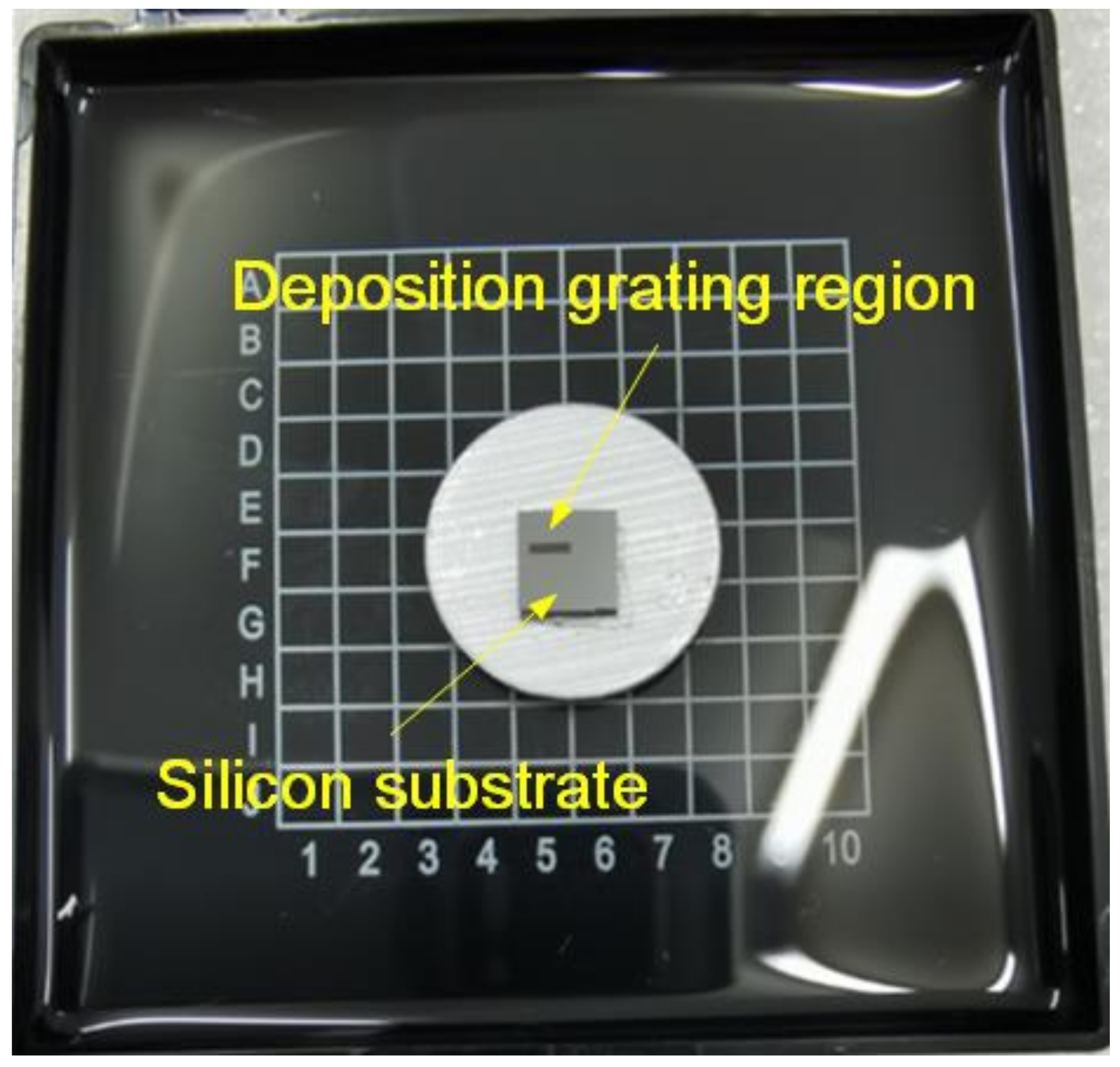
Atomic deposition grating is a new type of nanometer metrological transfer reference material. It is prepared by laser cold atomic deposition technology, which possesses a large deposition range and high accuracy. Therefore, the measuring equipment must have a large range and high precision measurement capability. Optical methods and ordinary AFM can no longer meet the requirements. In this paper, the atomic deposition grating standard template manufactured by Tongji University is measured by the target instrument, which achieves accurate characterization and evaluation of the grating structure up to 1 mm.
Figure 12 shows the atomic deposition grating sample. The standard grating period is 212.8 nm, half the length of a 425.6 nm laser.
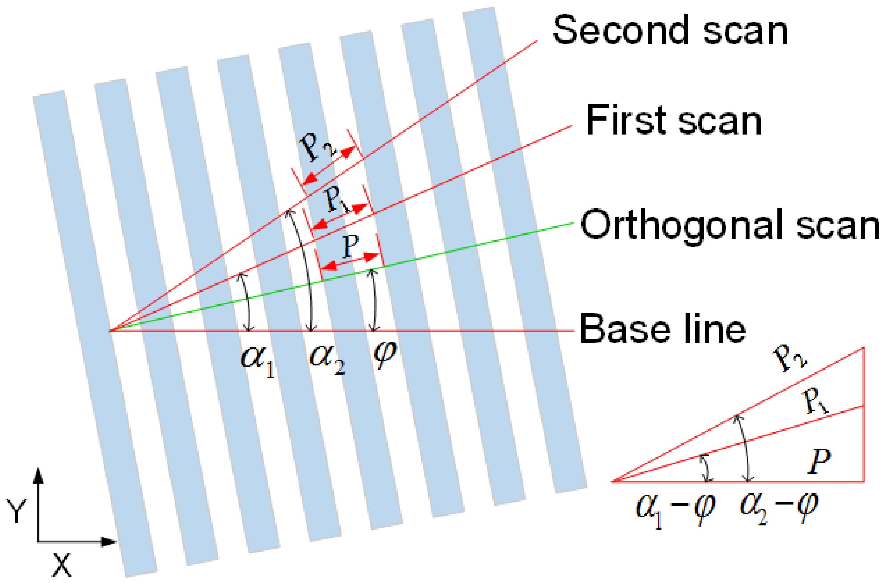
In grating measurement, the scanning angle greatly influences the measurement result. If the scanning angle is not orthogonal, the measurement result will introduce cosine error. In this paper, the method of twice measurement is used to extract the orthogonal angle, and the measurement results are corrected by using the extracted orthogonal angle. The scanning method is shown in
Figure 13.
Place the sample on the table with
α1 angle for the first scan to obtain the cycle value
P1. Rotate the sample with
α2 angle to obtain the cycle value
P2. Then, calculate the orthogonal angle
φ according to Formula (4). Correct
P1 or
P2 with Formulas (5) or (6) to obtain the accurate value of grating period
P.
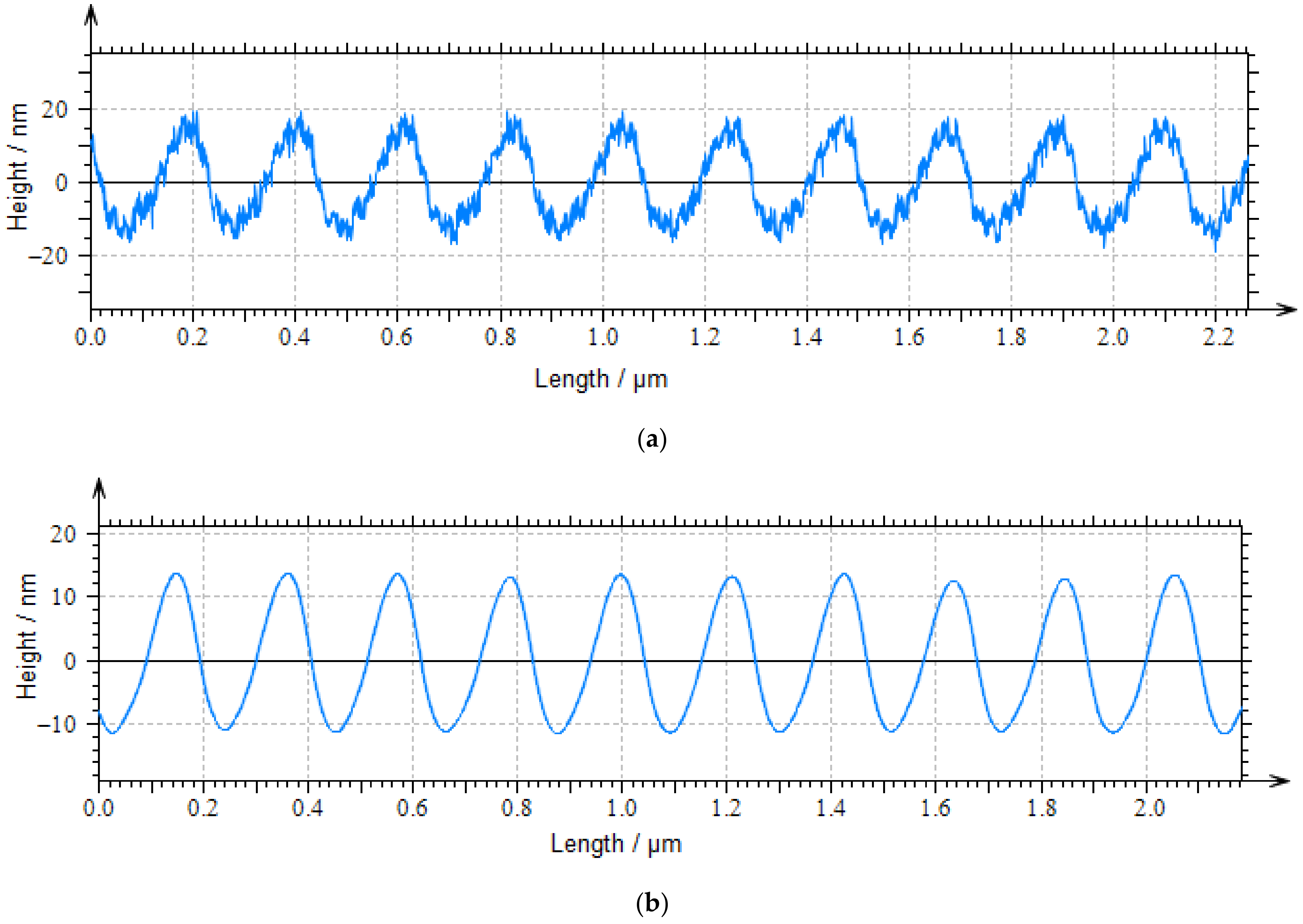
An AR5-NCLR probe with a length diameter ratio of 1:5 is used for grating measurement. The scanning range is 1 mm, the sampling interval is 10 nm, and the scanning speed is 8 μm/s. After ten repeated measurements, the results are calculated using the fast Fourier transform method, which obtains the grating period of 212.7 nm, and the standard deviation is 0.3 nm.
Figure 14 shows the grating profile of ten cycles from the measurement results. The measurement uncertainty is analyzed as follows:
Where ux is the uncertainty introduced by the x direction motion error of the laser interferometer. uz and up can be neglected in transverse dimension measurement.
The combined standard uncertainty can be described as
According to Equation (7) and
Table 2, the combined standard uncertainty of 0.30 nm can be calculated. In addition, the expanded uncertainty is 0.60 nm (
k = 2). The measurement result of the grating sample is (212.7 ± 0.6) nm (
k = 2).
Through the uncertainty analysis results of step and grating, it can be found that the measurement repeatability is the main factor affecting the uncertainty. The low repeatability of the grating measurement is due to the large measurement range and the average effect. The more periods included, the smaller the average deviation was obtained. The pitch is calculated using the full data length of 1 mm by the FFT method. Nearly 4700 periods are included in the calculation. The uncertainty components are derived from our historical data and taken to a conservative value.
3.3. Tool Tip Measurement
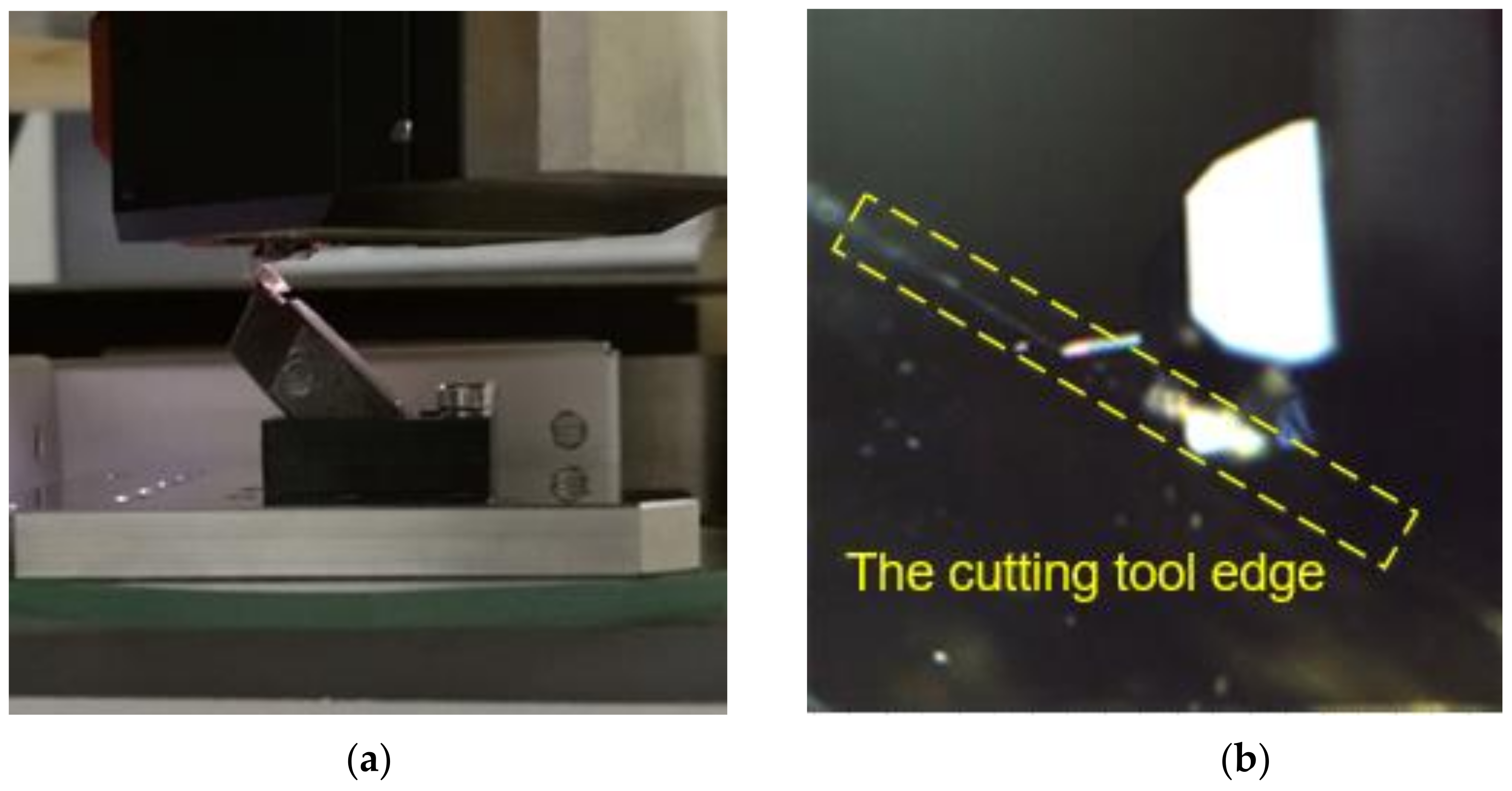
It is a significant ultraprecision machining method that uses hard cutting tools to process nonferrous and non-metallic materials. The quality of the cutting edge and surface of cutting tools directly affects the surface quality integrity of the machined parts. In the cutting process, the tool tip arc profile error will ‘copy’ to the workpiece profile, which has a crucial impact on the workpiece surface accuracy. In this paper, the constructed AFM system is used to measure the profile of the tool edge, and the tool tip profile with a large range of 1.5 mm is characterized.
Figure 15 shows a photo of the measurement process. The cutting tool is fixed on a metal base. The base is clamped at a special angle by a mold manufactured by 3D printing.
During the measurement, set the scanning range to 1.5 mm, the sampling interval to 100 nm, and the scanning speed to 10 μm/s, and obtain the original contour of the tool tip as shown in
Figure 16.
A Gaussian filter with a cut-off frequency of 0.08 mm is used for high-pass filtering to separate the ripple and roughness information of the tool tip. Then a Gaussian filter with a cut-off frequency of 0.025 mm is used for low-pass filtering to separate the circular arc ripple of the tool tip, as shown in
Figure 17. After calculation, the
Ra and
Rz values of the tool tip arc ripple are 29.8 nm and 189 nm, respectively.
5. Conclusions
The measurement range of the metrological atomic force microscope system constructed in this paper covers three scales, i.e., millimeter, micrometer, and nanometer, which can realize the large scale and high precision measurement of microstructure. By designing a low noise amplifier circuit, the noise of the measurement system is effectively reduced, and the measurement accuracy is guaranteed. The system achieves the measurement range of 25 mm × 25 mm × 5 mm, and the noise is lower than 2 nm. The experiments on the ultrahigh step, atomic deposition grating, and cutting tool sample were carried out by the proposed measurement system, which verified the measurement capability in a large range with high precision. The measurement system can meet the surface measurement requirements of most conventional micro/nano standard artifacts and some complex micro structures and devices, which can serve the semiconductor, micro/nanomanufacturing, and other fields. It can provide large scale, high precision, traceable testing, and calibration services for relevant research institutions and enterprises.
