Abstract
The efficiency of thin film photoelectric devices can be improved by redirecting incident electromagnetic radiation along their surface layers. Redirection can be achieved using antireflection coatings made of subwavelength dielectric particle arrays. In this study, we fabricate such coatings, consisting of Ge particles on quartz glass substrates via solid-state dewetting, transforming thin Ge films into compact particles. Using optically transparent substrates, we measure reflection and transmission spectra and determine absorption spectra, showing that substrates coated with Ge particles absorb much more strongly than substrates coated with continuous Ge films. The spectra obtained using objective lenses with different aperture angles indicate that scattered radiation is predominantly directed at glancing angles to the substrate surface. The lateral propagation of scattered radiation is the result of destructive interference, which suppresses both reflected and transmitted radiation.
1. Introduction
Coatings made of continuous dielectric films and/or textured surfaces [1,2,3,4] possess excellent antireflective properties and are an integral part of the majority of optical elements and photoelectric devices [5,6,7,8]. They do not practically alter the direction of incident electromagnetic (EM) radiation propagation in the substrate. Coatings made of compact dielectric particles also exhibit antireflective properties, but can change the direction of incident EM radiation. By directing a part of the scattered EM radiation along the substrate surface layers, they allow the use of thinner functionally active surface layers to achieve the same level of incident radiation absorption as thick layers [9,10,11,12]. The change in the propagation direction of scattered radiation occurs due to the action of several factors. The strongest effect arises from the interference of incident radiation with the fields of magnetic and electric Mie resonances excited in the particles [1,13,14,15,16,17,18,19,20]. This interference can suppress both reflected and transmitted radiation [21,22,23,24,25] and, as a result, direct a significant part of it along the substrate surface layers [26]. In structures with periodic lattices of dielectric particles, this part of scattered radiation can experience collective lattice resonances due to Wood’s anomalies [23,27,28,29,30,31,32]. Experimentally, these resonances are observed as absorption peaks, which quantitatively characterize this part of the radiation [32]. Another effect is associated with the interference of resonance modes excited in particles when they are located close to each other at a distance of ~500 nm or less. In this case, the role of quadrupole resonances, the effect of which can exceed the effect of dipole resonances when the distance between particles becomes less than 200 nm, increases [26].
One of the simplest methods for obtaining coatings consisting of dielectric particles is based on the use of the dewetting phenomenon, in which the deposited film is transformed into an array of compact particles on the nonwettable substrate surface upon annealing. The dewetting phenomenon can be solid-state when it occurs at temperatures well below the melting points of the deposited material. SiO2 surfaces are nonwettable for thin Ge and Si films [33,34,35,36,37,38]. The dewetting forms the particles, which often acquire a shape close to a sphere segment [36,39]. At the same time, Ge particles are characterized by a significantly larger vertical aspect ratio, AR = h/d (≥0.5) [36], than Si particles, where h is the particle height and d is their diameter. This makes Ge particle coatings more effective, since the spectral positions of the magnetic and electric dipole resonance maxima for particles with AR > 0.5 are closer to each other and, at certain AR values, their positions may coincide [19,20,40,41]. In this case, the interference of the resonance modes with the incident radiation leads to a greater suppression of the reflected and transmitted radiation, according to the Kerker conditions [17,18,22].
The reflection spectra of Ge particle coatings, obtained through the solid-state dewetting phenomenon on oxidized Si surfaces, showed broadband antireflection properties depending on the size of Ge particles [42]. The broadband antireflection was achieved due to three factors: (1) a wide particle size distribution, as the particle size determines the spectral positioning of Mie resonances; (2) weak dependence of the resonance position on the size of the particles located on the substrate when the particle size is less than 300 nm [20,42]; and (3) relatively small spatial gaps between particles (200 nm or less), at which the influence of quadrupole resonances increases [26], thus, extending the antireflection properties to the short-wavelength region. Since dielectric particle coatings lead to a change in the direction of scattered radiation, it is of interest to estimate the amount of such EM radiation depending on the particle size. This estimate can be obtained from the dependence of the absorption spectra on the propagation direction of scattered radiation.
In this study, we fabricated coatings consisting of subwavelength Ge particles on fused quartz substrates by exploiting the solid-state dewetting phenomenon. Transparent substrates were chosen to allow transmission spectra to be measured. By measuring the reflection (R) and transmission (T) spectra, the absorption spectra (A = 1 − R − T) were determined. Such formally determined absorption spectra revealed that the absorption in the samples coated with Ge particles was significantly stronger than in samples coated with a film containing the same amount of Ge. The spectra were measured using a microscope-spectrophotometer (MSFU-K, LOMO, Saint Petersburg, Russia). Their dependence on the aperture angle of the objective lens used showed that more than 30% of the incident radiation is scattered at glancing angles to the substrate surface. This part of the scattered radiation can increase the efficiency of photoelectric devices based on the use of thin surface layers.
2. Experimental
Quartz glass plates 0.5 mm thick were used as substrates. After the chemical cleaning of the quartz surface, the Ge deposition was carried out in an ultrahigh vacuum chamber, with a base pressure of about 1 × 10⁻⁸ Pa, manufactured by Omicron NanoTechnology GmbH (Limburg, Germany). A Knudsen cell with a BN crucible was used for the Ge deposition at a rate of ~0.6 nm/min, the same as in [42]. After the substrate degassing by the heating in the growth chamber at about 350 °C, the Ge deposition was performed without substrate annealing, i.e., at room temperature (RT). To initiate the solid-state dewetting process, the sample was annealed in the vacuum chamber to a temperature of about 500 °C for 1 h by the radiation from a heater located from the rear substrate side. The substrates coated at RT with Ge films of various thicknesses were also prepared.
The sample surface morphology was studied with a Raith Pioneer system (Raith GmbH, Dortmund, Germany) operated in a scanning electron microscope (SEM) mode. The SEM images of the samples obtained at a normal electron beam incidence were used to determine the particle size distributions using the ImageJ software (version 1.53e). The particle shape was observed at glancing electron beam incident angles, similar to that in [42]. The reflection (R) and transmission (T) spectra at a normal light incidence were measured with the microscope-spectrophotometer MSFU-K in the spectral range from 400 to 1100 nm. To obtain information about the angular distribution of scattered light, we used objectives with magnifications of 5, 10, 20, 40 and 100×, and numerical apertures (N.A.) of 0.1, 0.3, 0.45, 0.65 and 0.8, respectively, which have aperture angles (α) of about 5.7, 17.4, 27.7, 40.5 and 53.1 degrees calculated from the ratio N.A. = sin α. When measuring the transmission spectra, the incident light beam divergence was limited by collimation diaphragms and did not exceed 2 degrees. The spectra presented in the figures were measured using an objective with N.A. = 0.3, except for the figure showing the dependence of the spectra on the aperture angle.
3. Experimental Results
The Ge deposition on the SiO2 surface at elevated temperatures results in the formation of compact particles without the creation of a wetting layer. The solid-state dewetting phenomenon also occurs during the annealing of thin Ge films initially deposited on SiO2 at relatively low temperatures (<300 °C). The minimum temperature required for the formation of compact Ge particles is about 350 °C [42]. In this work, to complete the dewetting process and compact particle formation, the annealing of Ge films was performed at 500 °C in a vacuum chamber right after the Ge deposition (Figure 1). It should be noted that compact particles are formed by the decomposition of initial Ge films with a thickness of about 40 nm or less. During the decomposition of thicker films, some of the formed Ge particles are interconnected by bridges (Figure 1c).
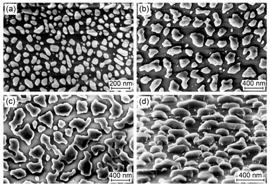
Figure 1.
SEM images of Ge particles formed by annealing Ge films deposited on quartz glass surfaces. The Ge film thickness was 15, 40, 50 and 31 nm in (a–d), respectively. The SEM images were taken for (a–c) at an e-beam incident angle of 90 degrees and for (d) at an angle of ~10 degrees to the substrate surfaces.
The Ge particle formation was studied previously on Si substrates coated with a thin SiO2 film. The SEM images obtained there showed that the Ge particle shape is close to spherical or hemispherical [42]. The formation of Ge particles on quartz substrates occurs in a similar way. The SEM images in Figure 1 show that the Ge particles acquire a rounded shape, while the shape of some relatively smaller particles is also close to spherical and hemispherical. At the same time, the particles of a relatively large size have some deviations from this shape. This is due to the atomic smoothness of the quartz surface, which is less than that of the Si substrate surface coated with a SiO2 film. Particles of rounded shape occupy the smallest area on the substrate and are less likely to merge with neighboring particles. The SEM images of the particles taken at the normal electron beam incidence angle give the particle shape projections onto the substrate. Their use for estimating the total substrate surface area occupied by the particles allows us to obtain somewhat larger values than the area occupied by particle bases. This also applies when determining the size of particles to obtain their size distributions, examples of which are shown in Figure 2.
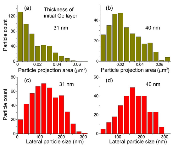
Figure 2.
Distributions of Ge particles as a function of (a,b), the area they occupy on the substrate, and (c,d), their diameter. The particles were obtained by annealing Ge films with a thickness of 31 and 40 nm, as noted in the corresponding graphs.
The size distributions of the areas occupied by each particle on the substrate surface, obtained from SEM images, are shown in Figure 2a,b. The distribution of particles as a function of the lateral size of their projection on substrates (Figure 2c,d) was determined under the assumption that it has a round shape, that is, it was calculated as the particle projection diameter. The obtained data show that the particle diameter distribution is characterized by a broad maximum. This means that particles of different sizes are formed, from a diameter of several tens to hundreds of nanometers, depending on the Ge amount in the initial film. Due to the difference in the atomic smoothness of the surface of fused quartz and Si coated with a thin SiO2 film, the size distribution of Ge particles on quartz substrates is wider than on the SiO2 films [42].
When Mie resonances are excited in Ge particles, the absorption occurs by the Ge itself. To estimate the portion of incident radiation that was not transmitted but absorbed by Ge, the reflection and transmission spectra of Ge films were measured. The samples coated with the films exhibit a strong reflection, which was about 50% (Figure 3a). The strong reflection significantly reduces the sample transmission, which for this reason only partially characterizes the Ge transmission (Figure 3b). To eliminate the influence of reflection on the transmission, the transmission spectra must be normalized to the amount of non-reflected radiation as Tfilm = T/(1 − R).
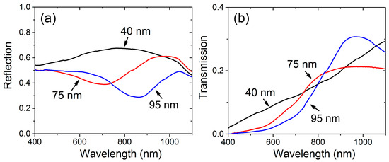
Figure 3.
(a) Reflection and (b) transmission spectra of Ge films deposited on quartz glass substrates at RT. The Ge film thicknesses were 40, 75 and 95 nm, marked in the figure for each spectrum.
The reflection and transmission spectra of the substrates coated with Ge particles are shown in Figure 4a,b. These samples are characterized by a much lower reflection (~0.15) compared to the reflection of Ge films. However, they are more reflective than Ge particle coatings obtained on the oxidized Si substrates [42]. In addition, these reflection spectra do not contain well-defined minima caused by the spectral positions of the Mie resonances. This is due to the wider size distribution of Ge particles on quartz substrates (Figure 2). Despite the lower reflection of Ge particle coatings than that of Ge films, it remains higher compared to the reflection of the bare quartz surface, which was about 4% and corresponded to [43].
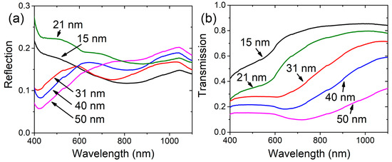
Figure 4.
(a) Reflection and (b) transmission spectra of samples with coatings made of particles obtained by the annealing of Ge films with thicknesses 15, 21, 31, 40 and 50 nm, marked in the figure for each spectrum.
The transmission spectra have a stronger dependence on the particle size. They differ significantly from the spectra obtained from coatings as continuous Ge films (Figure 3b). The Ge particles obtained as a result of the implementation of dewetting phenomenon are located at small distances from each other, which is 100–200 nm, depending on the particle size (Figure 1). At such small distances, the role of interaction between the fields of resonance modes excited in neighboring particles increases. In this case, the influence of quadrupole resonances, which are located in a shorter wavelength region than dipole resonances, becomes strong [26]. This explains the presence of stronger effects associated with Mie resonances in short-wavelength regions, despite the increase in the size of Ge particles obtained from thicker Ge films. Note that the reduction in the transmission due to the absorption by the quartz substrate itself is insignificant, since after excluding the contribution of reflection from the quartz surface for our samples it is about 2% and is consistent with [44].
The absorption spectra of coatings consisting of Ge particles, formally obtained from the reflection and transmission spectra as A = 1 − R − T, are shown in Figure 5. They exhibit strong absorption, which is associated mainly with both absorption by the Ge particles themselves and with a change in the scattered light direction due to the interference of the incident radiation with the fields of dipole and quadrupole resonance modes. The part of the scattered radiation propagating at glancing angles to the substrate surface does not enter the detector and is recorded as absorbed.
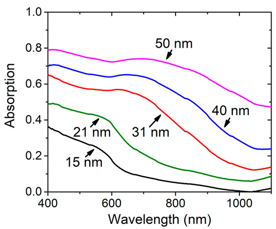
Figure 5.
Absorption spectra of quartz glass substrates coated with Ge particles obtained by the annealing of Ge films with thicknesses 15, 21, 31, 40 and 50 nm, marked in the figure for each spectrum.
To obtain the data on the propagation direction of the scattered radiation, the reflection and transmission spectra were measured depending on the aperture angle of the objective lens (Figure 6a,b). The measured spectra turned out to be practically independent of the α value; for α up to ~53 degrees, the absorption decreases by less than 5% in a wide spectral range (Figure 6). This only slightly exceeds the scatter in the measured values, which is about 3%, and is mainly determined by the inhomogeneity of particle distribution over the substrate surface, since the surface area used in the measurements does not remain the same after changing the objective lens. The spectra in Figure 6 show the data for a Ge particle coating obtained by annealing a 40 nm thick Ge film. The spectra of coatings obtained from Ge films of other thicknesses exhibit similar dependences on α.
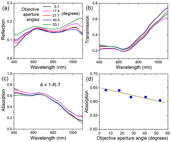
Figure 6.
Objective aperture angle dependence of (a) reflection, (b) transmission and (c) absorption spectra, and (d) absorption at a wavelength of 600 nm of a quartz glass substrate coated with Ge particles obtained by annealing a 40 nm thick Ge film. The angle values for the corresponding spectra are shown in (a).
The coatings consisting of Ge particles absorb significantly stronger than films containing the same amount of Ge (Figure 7). Using SEM images, it was determined that the Ge particles obtained from the 31 nm thick Ge film occupy 34% of the substrate surface. This corresponds to an average thickness of Ge in particles of about 91 nm, since Ge does not evaporate from the substrate surface at the annealing temperature of 500 °C and completely transforms into particles. This average thickness corresponds well to the 95 nm thick Ge film, which we can use to compare absorption properties. This film must occupy ~33% of the substrate surface to contain the same amount of Ge as the particles obtained from the 31 nm thick Ge film, while the rest of the substrate surface must remain uncoated with Ge.
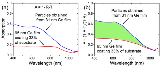
Figure 7.
Absorption spectra of the quartz glass substrates coated with Ge particles obtained by annealing a 31 nm thick Ge film and partly coated with a 95 nm thick Ge film, marked in the figure at the corresponding spectra. The spectra in (a) show the absorption obtained as A = 1 − R − T and the spectra in (b)—as A = (1 − R − T)/(1 − R).
The reflection of the samples coated with Ge films is much stronger than the reflection of the samples coated with particles (Figure 3a and Figure 4a). To eliminate the difference in reflection, the absorption spectra were normalized to the unreflected radiation intensity. The comparison of the spectra in Figure 7b shows that, in the range of 400–700 nm, the coating consisting of Ge particles absorbs approximately twice as much EM radiation as the same amount of Ge in the form of a film. This difference is not only due to the stronger absorption of Ge in the particles. This is also the result of the difference in the direction of the scattered radiation propagation, at which the significant part of radiation scattered by Ge particle coatings does not enter the objective lens. It is scattered at angles greater than the objective aperture angles. The data obtained show that the significant part of the incident radiation is scattered at angles close to the grazing angles or along the substrate surface layers.
The particles obtained from a 31 nm thick Ge film have an average diameter (d) size of about 130 nm (Figure 2c). The position of the reflection minimum of coatings consisting of Ge particles associated with dipole Mie resonances is determined by the relation λdip = neffd, where neff is the effective refractive index of the particle material, which depends on the particle size [20]. In our case, the maximum scattering, which can be attributed to dipole excitations, is in the wavelength range of about 650 nm (Figure 7). This corresponds to neff ≈ 5. This is consistent with the previously obtained data that, for particles of up to 300 nm in size, neff has a value greater than the refractive index of the particle material [20,42]. In the shorter wavelength range, scattering is determined by the excitation of quadrupole resonances, the action of which becomes stronger than that of dipole ones when the distance between them is less than 200 nm [26]. Such distances between particles are observed in our case (Figure 1). This determines the strong scattering of incident radiation in the short wavelength range (Figure 7).
Resonances in particles made of high-n materials are characterized by higher quality factors and larger extinction values [45,46,47]. Among single-element materials widely used in the conventional Si technology, Si and Ge have high refractive indexes, and the n value of Ge in the visible and IR regions is higher than the n value of Si. This allows the use of smaller Ge particles to produce Mie resonances at given wavelengths. In this case, smaller particles occupy less substrate surface area. These properties make coatings made of Ge particles promising for use not only in the IR, but also in the visible region, where Ge is characterized by a rather high absorption coefficient.
The spatial distribution of Mie resonance scattering was measured for single Si particles in the millimeter range [12]. In the visible range, the radiation spectra were obtained for the forward and backscattering for single Si particles [15,48], as well as Mie resonance-based coatings [1,22,24,42,49,50,51]. However, the spatial distribution of scattered radiation for nanosized dielectric particles was not measured, and information on the direction of scattered radiation for coatings is limited. Most theoretical studies are focused on the calculation of spatial distribution of magnetic and electric fields around the particles and the spectral position of magnetic and electric Mie resonance modes [21,23,25]. From the experimental results obtained here (Figure 7b), we can conclude that about 35% of the incident radiation propagates in the original direction, no more than 35% is scattered at angles less than 35 degrees to the substrate surface, and the remaining part of at least 30% is absorbed by Ge. Recently, when studying the Ge particle lattice, a surface lattice resonance was observed in which about 10% of the incident radiation participated. This part of scattered radiation propagates exclusively in the plane of the substrate surface layers [32]. In this case, a larger part of the incident radiation than here propagated at small angles to the substrate surface due to denser Ge particle arrays in the lattices. This part of scattered radiation can also be increased by using an additional protective antireflection coating, such as a Si3N4 film [1], which further reduces the reflection, as well as by utilizing a particle material that absorbs less than Ge and has a higher refractive index.
4. Numerical Simulation
Numerical simulation of the optical properties of Ge particle coatings on a quartz glass substrate was performed using the free dimensional finite difference time domain (3D FDTD) method by the commercial software package FullWave 2020.09-1 from RSoft-SYNOPSYS (Sunnyvale, CA, USA) [52]. The built-in material editor of the 3D FDTD method used the known data for the Ge refractive index [53], which are shown as a graph in [26]. The particles have a hemispherical shape and are distributed over the substrate surface, forming a rectangular lattice (inset in Figure 8a). Their size varies randomly with an average diameter d = 5 × HGe, where HGe is the thickness of initial Ge films.
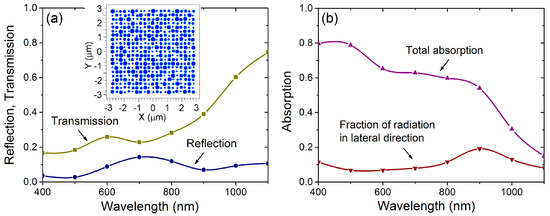
Figure 8.
Results of modeling by 3D FDTD. (a) The reflection and transmission spectra corresponding to the Ge particle coating obtained from a 40 nm thick Ge film. (b) The total absorption (A = 1 − R − T) and fraction of scattered radiation in the lateral direction. The insert in (a) is the scheme of the particle distribution over the substrate surface. This corresponds to 32% filling of the substrate with particles.
A plane wave is used to illuminate a rectangular area covered with particles. The simulation area in the X and Y coordinates is twice the area occupied by the particles to observe the full scattering field. The Z-direction simulation domain is selected so that the FDTD monitors can measure the transmitted and reflected power to collect the power flux within the scattering angle corresponding to the objective with N.A. = 0.65. The simulation also allows one to obtain the fraction of radiation in lateral directions (Figure 8b), which is determined by subtracting the internal absorption by Ge particles, also calculated, from the total absorption. It can be noted that this lateral radiation fraction corresponds well to the direct numerical measurement of the total lateral scattering using multiple power monitors placed at the X and Y boundaries of the simulation domain.
The results of numerical simulation generally agree well with the experimental data. It should be noted that the shape of real and simulated Ge particles is rather different, so the current simulation does not fully match the experiments. However, it is an effective tool for studying the general properties of experimental structures. For example, the simulations confirm the experimental data that the absorption varies smoothly over a wide wavelength range and decreases only at longer wavelengths. The simulation also confirms that the absorption decreases with decreasing particle size, and the edge of the strong change in absorption shifts toward shorter wavelengths, similar to the experimental data in Figure 5. The simulations show that the lateral scattering is strong and varies up to 19% of incident radiation. This value is close to 10%, which was previously estimated from experimental results [32]. This part of scattered radiation, along with the scattered radiation propagating at glancing angles, can contribute to a significant increase of the optical absorption in the substrate surface layers, which is very promising for practical applications.
5. Conclusions
The coatings consisting of subwavelength-sized Ge particles were prepared using the solid-state dewetting process that transforms Ge films into compact particles on fused quartz substrates. These coatings increase the scattering of incident EM radiation due to its interference with the magnetic and electric Mie resonance modes excited in the particles. The significant part of scattered radiation does not come to the detector of the microscope-spectrophotometer, since it is directed at angles greater than the aperture angle of its objective. This is the part of the incident radiation propagating in the direction along the substrate surface or at glancing angles less than 37 degrees. The scattered radiation is broadband, due to the wide size distribution of Ge particles. In the short-wavelength range, it additionally originates from the excitation of quadrupole resonances, the role of which becomes significant at distances between particles less than 200 nm. The ability to increase the intensity of scattered radiation directed along the substrate surface layers makes it possible to increase the efficiency of thin film photoelectronic devices by creating conditions in them for a greater absorption of incident EM radiation.
Author Contributions
A.A.S. fabricated the structures and carried out the experiments. D.E.U. performed SEM measurements. Z.Z. carried out optical measurement. A.V.T. performed the numerical simulation. All authors discussed the results and analyzed the data. A.A.S. wrote the paper. All authors have read and agreed to the published version of the manuscript.
Funding
The work is supported by the Ministry of Science and Higher Education of the Russian Federation (project 075-15-2020-797 (13.1902.21.0024)).
Data Availability Statement
The data that support the findings of this study are available from the author upon reasonable request.
Acknowledgments
The authors acknowledge the Shared Equipment Centers CKP “NANOSTRUKTURY” of the Rzhanov Institute of Semiconductor Physics SB RAS and CKP “VTAN” (ATRC) of the NSU Physics Department for the instrumental and technological support.
Conflicts of Interest
The authors declare no conflict of interest.
References
- Spinelli, P.; Verschuuren, M.A.; Polman, A. Broadband omnidirectional antireflection coating based on subwavelength surface Mie resonators. Nat. Commun. 2012, 3, 692. [Google Scholar] [CrossRef]
- Duttagupta, S.; Ma, F.; Hoex, B.; Mueller, T.; Aberle, A.G. Optimised antireflection coatings using silicon nitride on textured silicon surfaces based on measurements and multidimensional modelling. Energy Procedia 2012, 15, 78. [Google Scholar] [CrossRef]
- Yelisseyev, A.; Fedyaj, V.; Simonov, V.; Isaenko, L.; Lobanov, S.; Shklyaev, A.; Simanchuk, A.; Babin, S.; Dostovalov, A. Femtosecond Laser Direct Writing of Antireflection Microstructures on the Front and Back Sides of a GaSe Crystal. Photonics 2022, 9, 774. [Google Scholar] [CrossRef]
- Sayed, H.; Al-Dossari, M.; Ismail, M.A.; Abd El-Gawaad, N.S.; Aly, A.H. Theoretical Analysis of Optical Properties for Amorphous Silicon Solar Cells with Adding Anti-Reflective Coating Photonic Crystals. Photonics 2022, 9, 813. [Google Scholar] [CrossRef]
- Chattopadhyay, S.; Huang, Y.F.; Jen, Y.J.; Ganguly, A.; Chen, K.H.; Chen, L.C. Anti-reflecting and photonic nanostructures. Mater. Sci. Eng. R Rep. 2010, 69, 1–35. [Google Scholar] [CrossRef]
- Keshavarz Hedayati, M.; Elbahri, M. Antireflective Coatings: Conventional Stacking Layers and Ultrathin Plasmonic Metasurfaces, A Mini-Review. Materials 2016, 9, 497. [Google Scholar] [CrossRef] [PubMed]
- Zhou, Z.X.; Ye, M.J.; Yu, M.W.; Yang, J.H.; Su, K.L.; Yang, C.C.; Lin, C.Y.; Babicheva, V.E.; Timofeev, I.V.; Chen, K.P. Germanium Metasurfaces with Lattice Kerker Effect in Near-Infrared Photodetectors. ACS Nano 2022, 16, 5994. [Google Scholar] [CrossRef]
- Ji, C.; Liu, W.; Bao, Y.; Chen, X.; Yang, G.; Wei, B.; Yang, F.; Wang, X. Recent Applications of Antireflection Coatings in Solar Cells. Photonics 2022, 9, 906. [Google Scholar] [CrossRef]
- Spinelli, P.; Polman, A. Light Trapping in Thin Crystalline Si Solar Cells Using Surface Mie Scatterers. IEEE J. Photovolt. 2014, 4, 554. [Google Scholar] [CrossRef]
- Amalathas, A.P.; Alkaisi, M.M. Nanostructures for Light Trapping in Thin Film Solar Cells. Micromachines 2019, 10, 619. [Google Scholar] [CrossRef]
- Zhu, B.; Chen, L.; Ye, S.; Luo, W. The Light-Trapping Character of Pit Arrays on the Surface of Solar Cells. Photonics 2023, 10, 855. [Google Scholar] [CrossRef]
- Lee, N.; Xue, M.; Hong, J.; van de Groep, J.; Brongersma, M.L. Multi-Resonant Mie Resonator Arrays for Broadband Light Trapping in Ultrathin c-Si Solar Cells. Adv. Mater. 2023, 35, 2210941. [Google Scholar] [CrossRef]
- Gomez-Medina, R.; Garcia-Camara, B.; Suarez-Lacalle, I.; Gonzalez, F.; Moreno, F.; Nieto-Vesperinas, M.; Saenz, J.J. Electric and magnetic dipolar response of germanium nanospheres: Interference effects, scattering anisotropy, and optical forces. J. Nanophotonics 2011, 5, 053512. [Google Scholar] [CrossRef]
- Geffrin, J.M.; García-Cámara, B.; Gómez-Medina, R.; Albella, P.; Froufe-Pérez, L.S.; Eyraud, C.; Litman, A.; Vaillon, R.; González, F.; Nieto-Vesperinas, M.; et al. Magnetic and electric coherence in forward- and back-scattered electromagnetic waves by a single dielectric subwavelength sphere. Nat. Commun. 2012, 3, 1171. [Google Scholar] [CrossRef] [PubMed]
- Evlyukhin, A.B.; Novikov, S.M.; Zywietz, U.; Eriksen, R.L.; Reinhardt, C.; Bozhevolnyi, S.I.; Chichkov, B.N. Demonstration of Magnetic Dipole Resonances of Dielectric Nanospheres in the Visible Region. Nano Lett. 2012, 12, 3749. [Google Scholar] [CrossRef]
- Moitra, P.; Slovick, B.A.; Li, W.; Kravchencko, I.I.; Briggs, D.P.; Krishnamurthy, S.; Valentin, J. Large-scale all-dielectric metamaterial perfect reflectors. ACS Photonics 2015, 2, 692. [Google Scholar] [CrossRef]
- Baryshnikova, K.V.; Petrov, M.I.; Babicheva, V.E.; Belov, P.A. Plasmonic and silicon spherical nanoparticle antireflective coatings. Sci. Rep. 2016, 6, 22136. [Google Scholar] [CrossRef]
- Babicheva, V.E.; Evlyukhin, A.B. Resonant lattice Kerker effect in metasurfaces with electric and magnetic optical responses. Laser Photon. Rev. 2017, 11, 1700132. [Google Scholar] [CrossRef]
- Visser, D.; Basuvalingam, S.B.; Desieres, Y.; Anand, S. Optical properties and fabrication of dielectric metasurfaces based on amorphous silicon nanodisk arrays. Opt. Express 2019, 27, 5354. [Google Scholar] [CrossRef]
- Utkin, D.E.; Anikin, K.V.; Veber, S.L.; Shklyaev, A.A. Dependence of light reflection of germanium Mie nanoresonators on their aspect ratio. Opt. Mater. 2020, 109, 110466. [Google Scholar] [CrossRef]
- Babicheva, V.E.; Evlyukhin, A.B. Resonant suppression of light transmission in high-refractive-index nanoparticle metasurfaces. Opt. Lett. 2018, 43, 5186. [Google Scholar] [CrossRef] [PubMed]
- Tian, J.; Luo, H.; Li, Q.; Pei, X.; Du, K.; Qiu, M. Near-Infrared super-absorbing all-dielectric metasurface based on single-layer germanium nanostructures. Laser Photon. Rev. 2018, 12, 1800076. [Google Scholar] [CrossRef]
- Zhang, X.; Li, J.; Donegan, J.F.; Bradley, A.L. Constructive and destructive interference of kerker-type scattering in an ultrathin silicon Huygens metasurface. Phys. Rev. Mater. 2020, 4, 125202. [Google Scholar] [CrossRef]
- Shklyaev, A.A.; Tsarev, A.V. Broadband antireflection coatings made of resonant submicron- and micron-sized SiGe particles grown on Si substrates. IEEE Photon. J. 2021, 13, 2200212. [Google Scholar] [CrossRef]
- Gerasimov, V.S.; Ershov, A.E.; Bikbaev, R.G.; Rasskazov, I.L.; Isaev, I.L.; Semina, P.N.; Kostyukov, A.S.; Zakomirnyi, V.I.; Polyutov, S.P.; Karpov, S.V. Plasmonic lattice Kerker effect in ultraviolet-visible spectral range. Phys. Rev. B 2021, 103, 035402. [Google Scholar] [CrossRef]
- Shklyaev, A.A.; Utkin, D.E.; Tsarev, A.V.; Kuznetsov, S.A.; Anikin, K.V.; Latyshev, A.V. Interdisk spacing effect on resonant properties of Ge disk lattices on Si substrates. Sci. Rep. 2022, 12, 8123. [Google Scholar] [CrossRef]
- Zakomirnyi, V.I.; Ershov, A.E.; Gerasimov, V.S.; Karpov, S.V.; Ågren, H.; Rasskazov, I.L. Collective lattice resonances in arrays of dielectric nanoparticles: A matter of size. Opt. Lett. 2019, 44, 5743. [Google Scholar] [CrossRef]
- Zakomirnyi, V.I.; Karpov, S.V.; Ågren, H.; Rasskazov, I.L. Collective lattice resonances in disordered and quasi-random all-dielectric metasurfaces. J. Opt. Soc. Am. B 2019, 36, E21. [Google Scholar] [CrossRef]
- Utyushev, A.D.; Zakomirnyi, V.I.; Ershov, A.E.; Gerasimov, V.S.; Karpov, S.V.; Rasskazov, I.L. Collective lattice resonances in all-dielectric nanostructures under oblique incidence. Photonics 2020, 7, 24. [Google Scholar] [CrossRef]
- Zhao, X.; Xiong, L.; Zhang, Z.; Li, G. High-Q out-of-plane Mie electric dipole surface lattice resonances in silicon metasurfaces. Opt. Express 2022, 30, 34601. [Google Scholar] [CrossRef]
- Zhang, Z.; Liu, P.; Lu, W.; Bai, P.; Zhang, B.; Chen, Z.; Maier, S.A.; Rivas, J.G.; Wang, S.; Li, X. High-Q collective Mie resonances in monocrystalline silicon nanoantenna arrays for the visible light. Fundam. Res. 2023, 3, 822. [Google Scholar] [CrossRef]
- Shklyaev, A.A.; Utkin, D.E.; Tsarev, A.V.; Latyshev, A.V. Effect of Mie resonances in coatings consisting of dielectric particles on the light propagation in substrate surface layers. Opt. Mater. 2023, 143, 114171. [Google Scholar] [CrossRef]
- Cheynis, F.; Bussmann, E.; Leroy, F.; Passanante, T.; Müller, P. Stress effects on solid-state dewetting of nano-thin films. Int. J. Nanotechnol. 2012, 9, 396. [Google Scholar] [CrossRef]
- Cheynis, F.; Leroy, F.; Passanante, T.; Müller, P. Agglomeration dynamics of germanium islands on a silicon oxide substrate: A grazing incidence small-angle X-ray scattering study. Appl. Phys. Lett. 2013, 102, 161603. [Google Scholar] [CrossRef]
- Ye, J.; Zuev, D.; Makarov, S. Dewetting mechanisms and their exploitation for the large-scale fabrication of advanced nanophotonic systems. Int. Mater. Rev. 2019, 64, 439. [Google Scholar] [CrossRef]
- Shklyaev, A.A.; Latyshev, A.V. Dewetting behavior of Ge layers on SiO2 under annealing. Sci. Rep. 2020, 10, 13759. [Google Scholar] [CrossRef]
- Lozovoy, K.A.; Korotaev, A.G.; Kokhanenko, A.P.; Dirko, V.V.; Voitsekhovskii, A.V. Kinetics of epitaxial formation of nanostructures by Frank–van der Merwe, Volmer–Weber and Stranski–Krastanow growth modes. Surf. Coat. Technol. 2020, 384, 125289. [Google Scholar] [CrossRef]
- Toliopoulos, D.; Fedorov, A.; Bietti, S.; Bollani, M.; Bonera, E.; Ballabio, A.; Isella, G.; Bouabdellaoui, M.; Abbarchi, M.; Tsukamoto, S.; et al. Solid-state dewetting dynamics of amorphous Ge thin films on silicon dioxide substrates. Nanomaterials 2020, 10, 2542. [Google Scholar] [CrossRef]
- Shklyaev, A.A.; Budazhapova, A.E. Submicron- and micron-sized SiGe island formation on Si(100) by dewetting. Thin Solid Film. 2017, 642, 345. [Google Scholar] [CrossRef]
- Staude, I.; Miroshnichenko, A.E.; Decker, M.; Fofang, N.T.; Liu, S.; Gonzales, E.; Dominguez, J.; Luk, T.S.; Neshev, D.N.; Brener, I.; et al. Tailoring Directional Scattering through Magnetic and Electric Resonances in Subwavelength Silicon Nanodisks. ACS Nano 2013, 7, 7824–7832. [Google Scholar] [CrossRef]
- Moitra, P.; Slovick, B.A.; Yu, Z.G.; Krishnamurthy, S.; Valentine, J. Experimental demonstration of a broadband all-dielectric metamaterial perfect reflector. Appl. Phys. Lett. 2014, 104, 171102. [Google Scholar] [CrossRef]
- Shklyaev, A.A. Coatings consisting of Ge particles on nonwettable Si oxide surfaces and their resonance reflection spectra. Thin Solid Film. 2023, 768, 139720. [Google Scholar] [CrossRef]
- Pfeiffer, K.; Schulz, U.; Tünnermann, A.; Szeghalmi, A. Antireflection Coatings for Strongly Curved Glass Lenses by Atomic Layer Deposition. Coatings 2017, 7, 118. [Google Scholar] [CrossRef]
- Zhao, Y.; Li, Q.; Wang, Z.; Dai, Z.; Chen, T. Microchannel Fabrication in Fused Quartz by Backside Laser-Induced Plasma Ablation Using 248 nm KrF Excimer Laser. Appl. Sci. 2019, 9, 5320. [Google Scholar] [CrossRef]
- Wang, Z.; Luk’yanchuk, B.; Yue, L.; Yan, B.; Monks, J.; Dhama, R.; Minin, O.V.; Minin, I.V.; Huang, S.; Fedyanin, A.A. High order Fano resonances and giant magnetic fields in dielectric microspheres. Sci. Rep. 2019, 9, 20293. [Google Scholar] [CrossRef] [PubMed]
- Tian, J.; Li, Q.; Belov, P.A.; Sinha, R.K.; Qian, W.; Qiu, M. High-Q all-dielectric metasurface: Super and suppressed optical absorption. ACS Photonics 2020, 7, 1436. [Google Scholar] [CrossRef]
- Babicheva, V.E.; Evlyukhin, A.B. Multipole lattice effects in high refractive index metasurfaces. J. Appl. Phys. 2021, 129, 040902. [Google Scholar] [CrossRef]
- Fu, Y.H.; Kuznetsov, A.I.; Miroshnichenko, A.E.; Yu, Y.F.; Luk’yanchuk, B. Directional visible light scattering by silicon nanoparticles. Nat. Commun. 2013, 4, 1527. [Google Scholar] [CrossRef]
- Xu, R.; Takahara, J. All-dielectric perfect absorber based on quadrupole modes. Opt. Lett. 2021, 46, 3596–3599. [Google Scholar] [CrossRef] [PubMed]
- Liu, L.; Zhang, F.; Murai, S.; Tanaka, K. Loss Control with Annealing and Lattice Kerker Effect in Silicon Metasurfaces. Adv. Photonics Res. 2022, 3, 2100235. [Google Scholar] [CrossRef]
- Yezekyan, T.; Zenin, V.A.; Thomaschewski, M.; Malureanu, R.; Bozhevolnyi, S.I. Germanium metasurface assisted broadband detectors. Nanophotonics 2023, 12, 2171–2177. [Google Scholar] [CrossRef]
- RSoft Photonic Device Tools. Version 2020-09-1. Available online: https://www.synopsys.com/photonic-solutions/rsoft-photonic-device-tools.html (accessed on 23 October 2020).
- Palik, E.D. Handbook of Optical Constants of Solids; Academic Press: Cambridge, MA, USA, 1998; pp. 1–999. [Google Scholar]
Disclaimer/Publisher’s Note: The statements, opinions and data contained in all publications are solely those of the individual author(s) and contributor(s) and not of MDPI and/or the editor(s). MDPI and/or the editor(s) disclaim responsibility for any injury to people or property resulting from any ideas, methods, instructions or products referred to in the content. |
© 2023 by the authors. Licensee MDPI, Basel, Switzerland. This article is an open access article distributed under the terms and conditions of the Creative Commons Attribution (CC BY) license (https://creativecommons.org/licenses/by/4.0/).