Bound States in the Continuum and Induced Resonances in a Simple Plasmonic Waveguide with Sensing Application

 , , , ,
Abstract
:1. Introduction
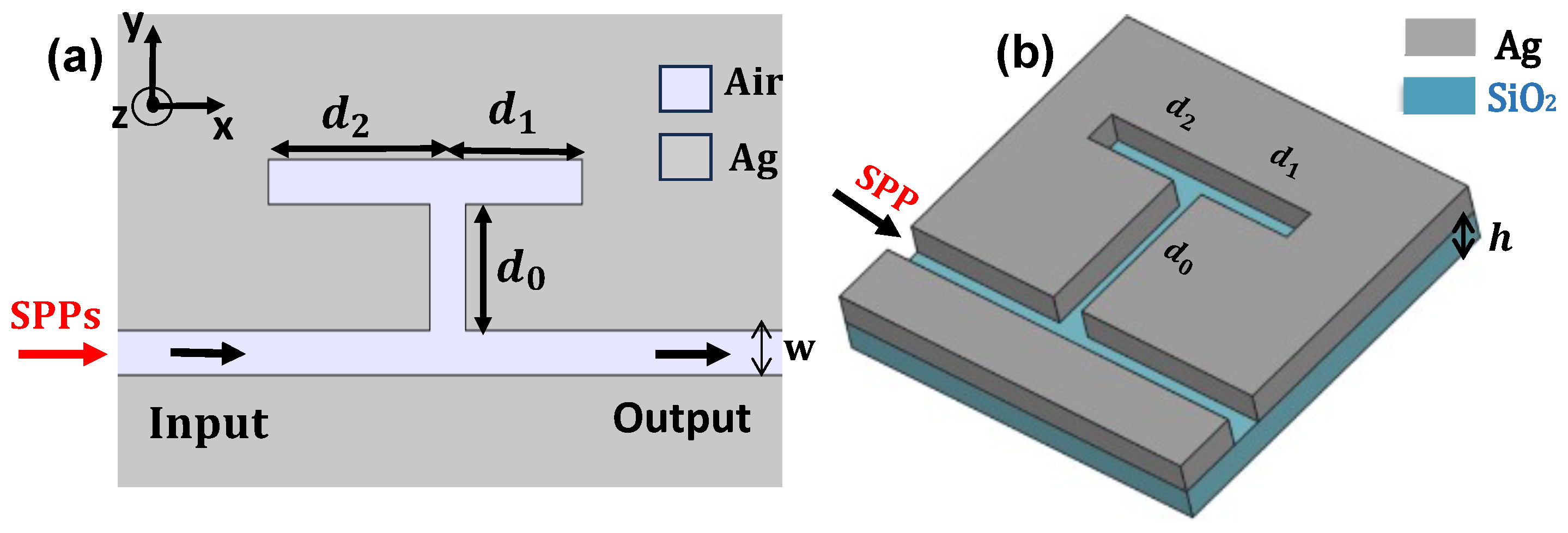
2. Basic Model and Theoretical Study
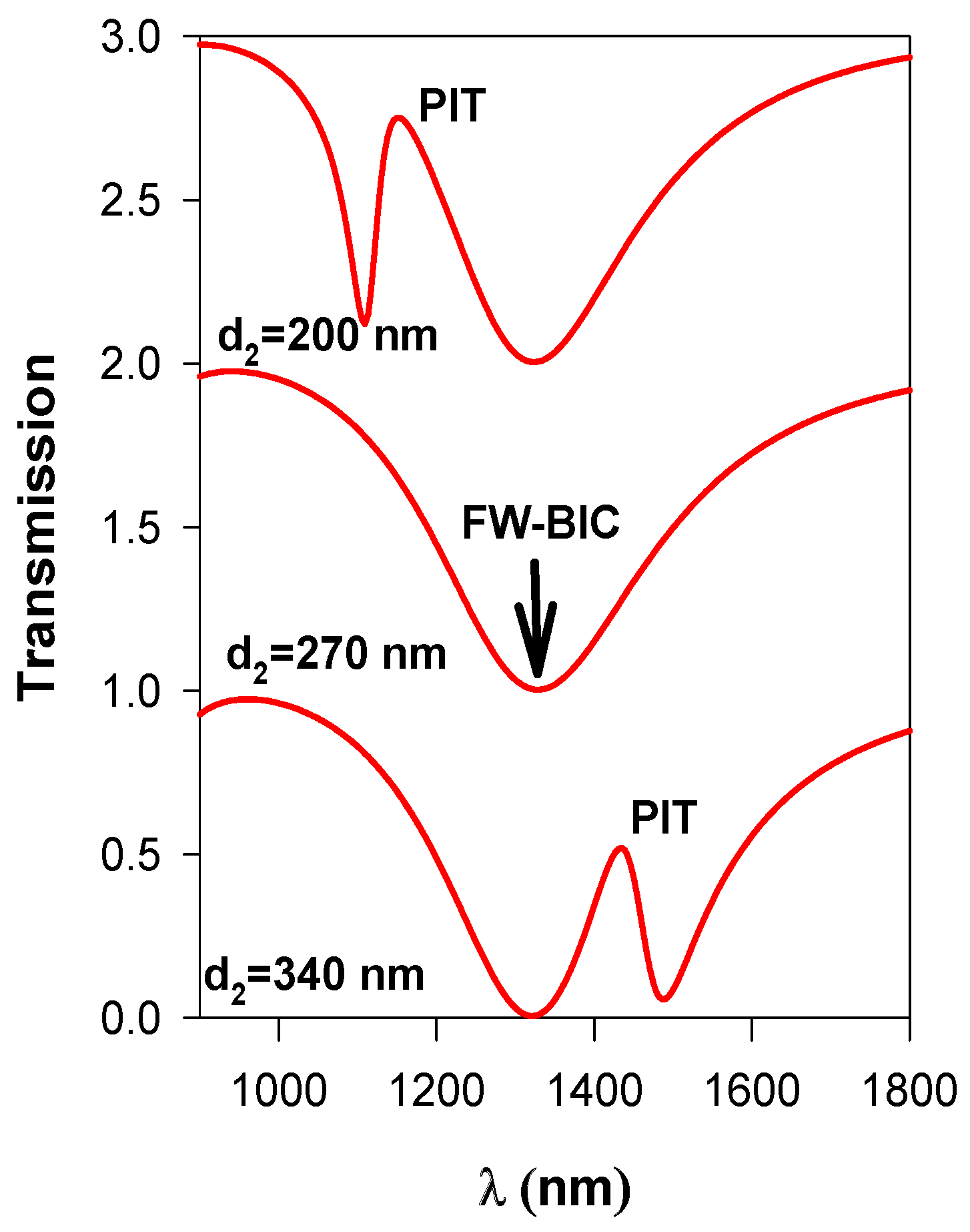
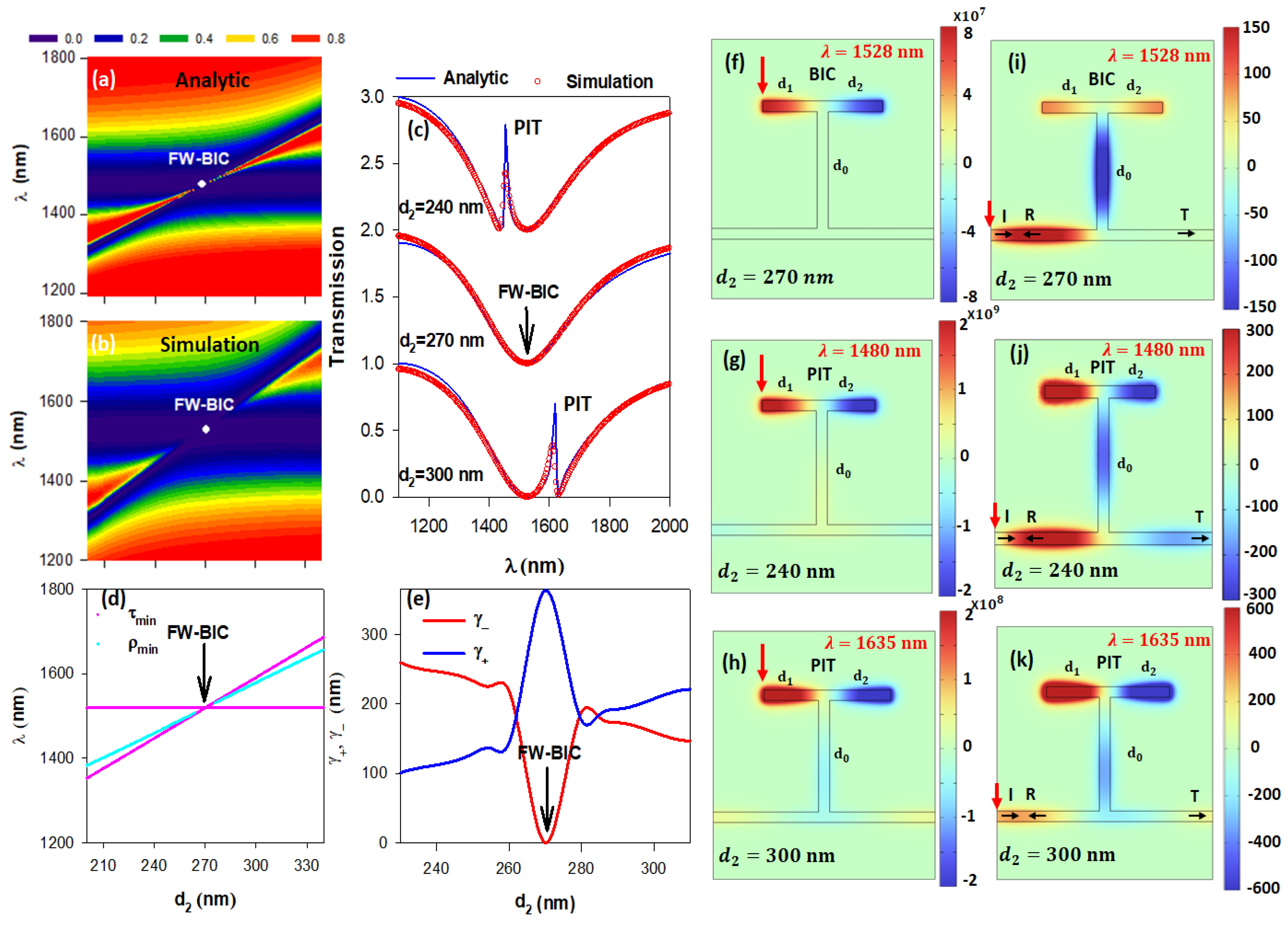
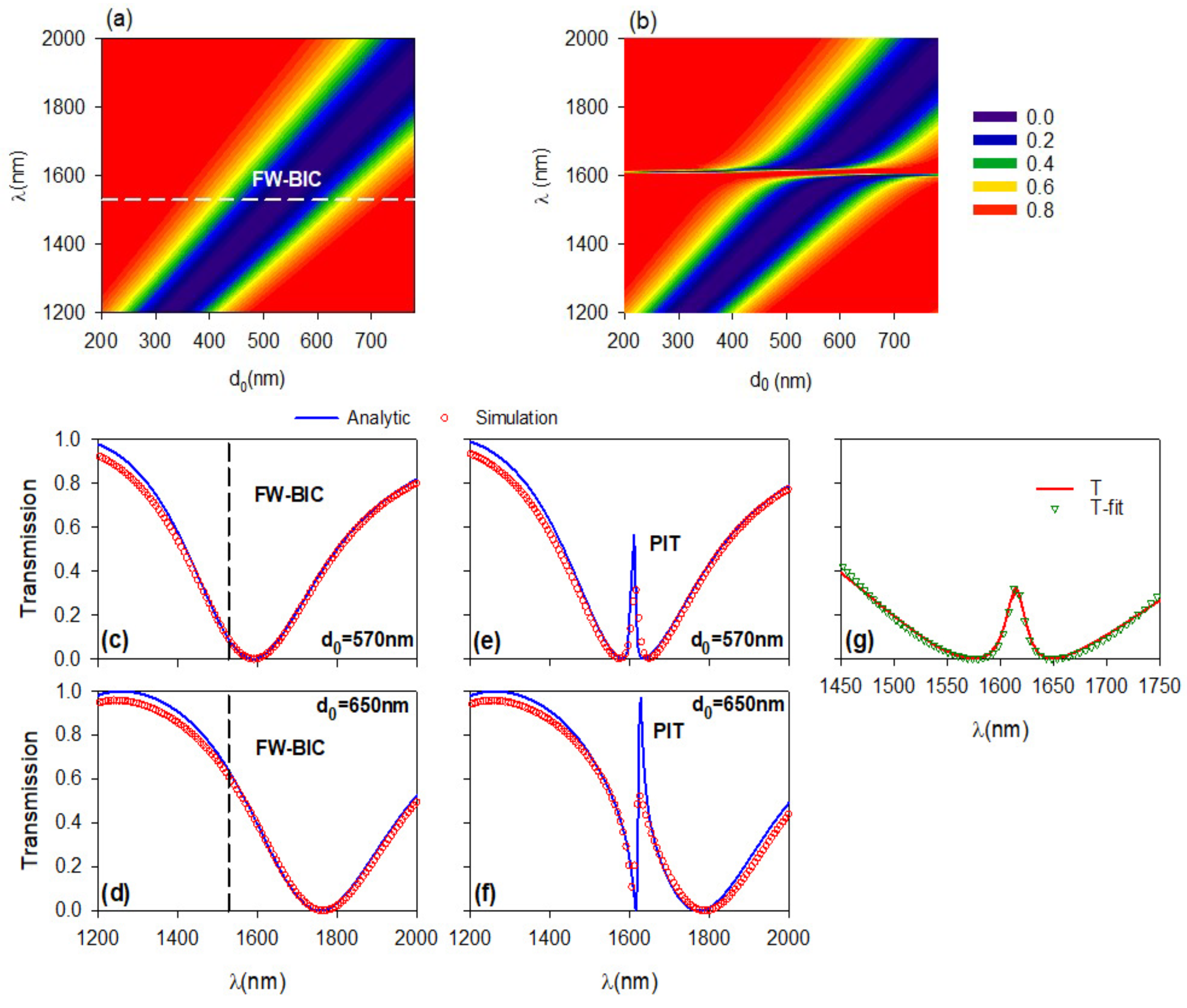
3. Numerical Analysis
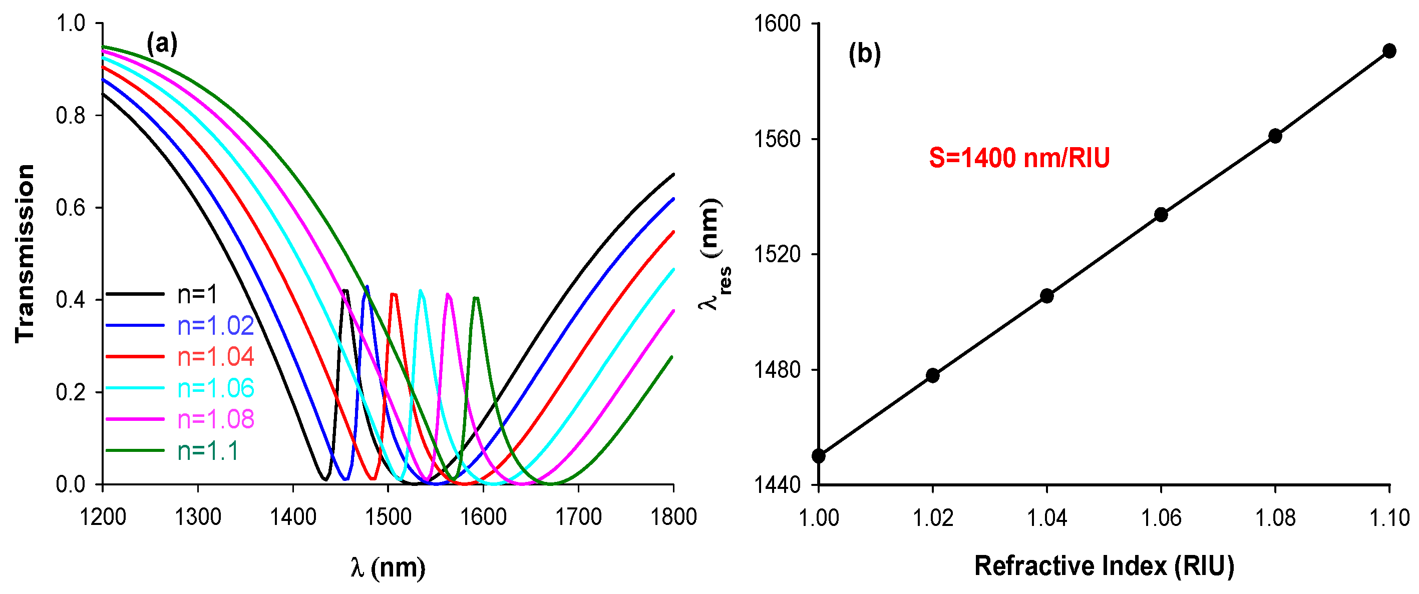
4. Sensing Applications
4.1. Gas Sensing
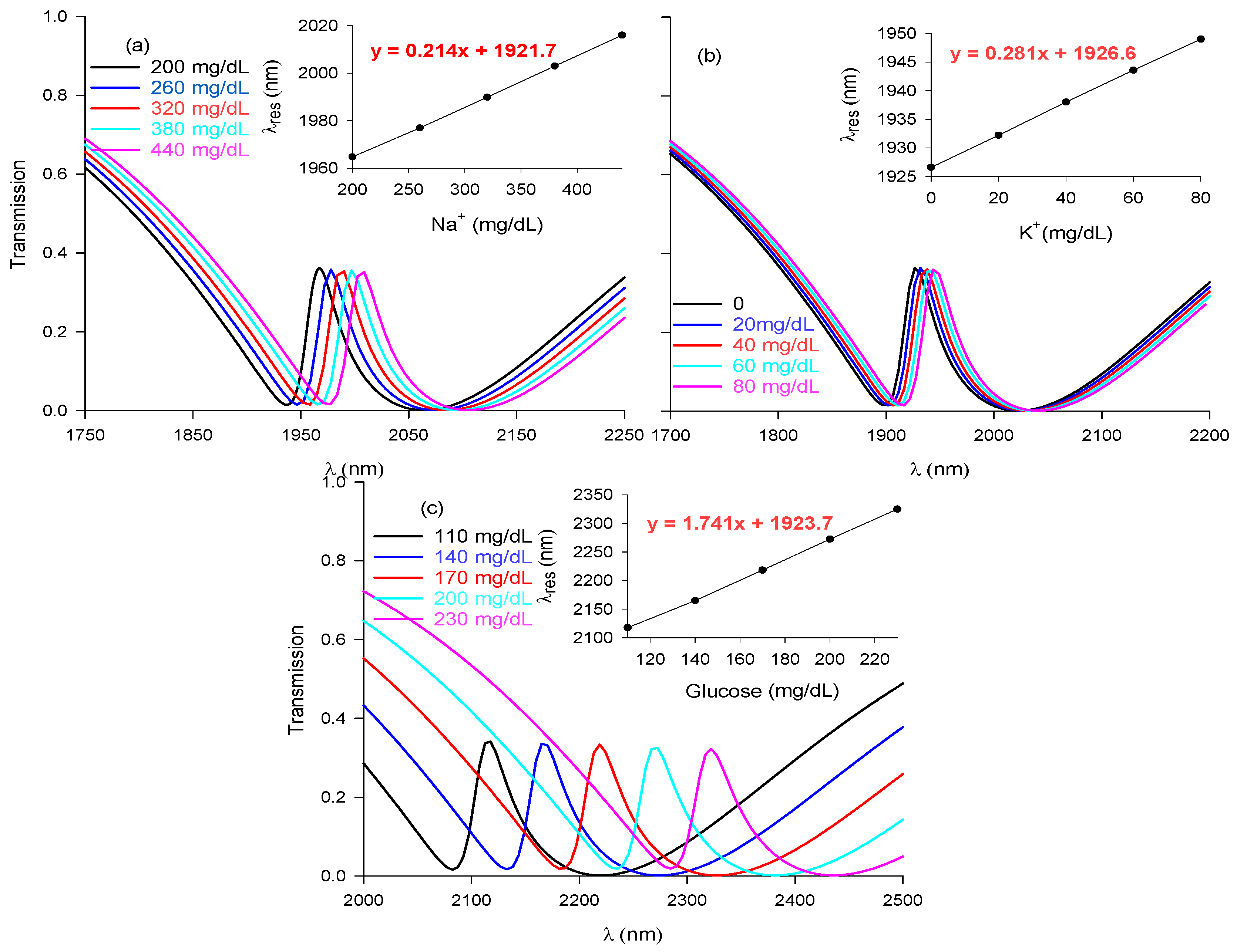
4.2. Biosensing
5. Conclusions
Author Contributions
Funding
Institutional Review Board Statement
Informed Consent Statement
Data Availability Statement
Conflicts of Interest
Appendix A. Numerical Results Based on Gold as a Metal
References
- Maier, S.A. Plasmonics: Fundamentals and Applications; Springer: New York, NY, USA, 2007. [Google Scholar]
- Ohashi, K.; Nishi, K.; Shimizu, T.; Nakada, M.; Fujikata, J.; Ushida, J.; Torii, S.; Nose, K.; Mizuno, M.; Yukawa, H.; et al. On-chip optical interconnect. Proc. IEEE 2009, 97, 1186–1198. [Google Scholar] [CrossRef]
- Barnes, W.L.; Dereux, A.; Ebbesen, T.W. Surface plasmon subwavelength optics. Nature 2003, 424, 824–830. [Google Scholar] [CrossRef] [PubMed]
- Oo, S.Z.; Silva, G.; Carpignano, F.; Noual, A.; Pechstedt, K.; Mateos, L.; Grant-Jacob, J.A.; Brocklesby, B.; Horak, P.; Charlton, M.; et al. A nanoporous gold membrane for sensing applications. Sens.-Bio-Sens. Res. 2016, 7, 133–140. [Google Scholar] [CrossRef] [PubMed]
- Saada, T.N.; da Silva, A.G.M.; Subramanian, P.; Pang, L.; Noual, A.; Djafari-Rouhani, B.; Mishyn, V.; Meziane, D.; Melinte, S.; Sandu, G.; et al. Plasmon-enhanced electrocatalytic oxygen reduction in alkaline media on gold nanohole electrodes. J. Mater. Chem. A 2020, 8, 10395–10401. [Google Scholar] [CrossRef]
- Fan, X. Sensitive surface plasmon resonance label-free biosensor on a fiber end-facet. Light Sci. Appl. 2022, 11, 325. [Google Scholar] [CrossRef] [PubMed]
- Dombi, P.; Pápa, Z.; Vogelsang, J.; Yalunin, S.V.; Sivis, M.; Herink, G.; Schàfer, S.; GroB, P.; Ropers, C.; Lienau, C. Strong-field nano-optics. Rev. Mod. Phys. 2020, 92, 025003. [Google Scholar] [CrossRef]
- Smirnov, V.; Stephan, S.; Westphal, M.; Emmrich, D.; Beyer, A.; Golzhauser, A.; Christoph, L.; Silies, M. Transmitting surface plasmon polaritons across nanometer-sized gaps by optical near-field coupling. ACS Photonics 2021, 8, 832–840. [Google Scholar] [CrossRef]
- Dionne, J.A.; Sweatlock, L.A.; Atwater, H.A.; Polman, A.J.P.R.B. Plasmon slot waveguides: Towards chip-scale prop-agation with subwavelength-scale localization. Phys. Rev. B 2006, 73, 035407. [Google Scholar] [CrossRef]
- Neutens, P.; Van Dorpe, P.; De Vlaminck, I.; Lagae, L.; Borghs, G. Electrical detection of confined gap plasmons in metal–insulator–metal waveguides. Nat. Photon. 2009, 3, 283–286. [Google Scholar] [CrossRef]
- Han, Z.; Forsberg, E.; He, S. Surface plasmon Bragg gratings formed in metal-insulator-metal waveguides. IEEE Photonics Technol. Lett. 2007, 19, 91–93. [Google Scholar] [CrossRef]
- Wen, K.; Yan, L.; Pan, W.; Luo, B.; Guo, Z.; Guo, Y.; Luo, X. Design of plasmonic comb-like filters using loop-based resonators. Plasmonics 2013, 8, 1017–1022. [Google Scholar] [CrossRef]
- Al Mahmud, R.; Sagor, R.H.; Khan, M.Z.M. Surface plasmon refractive index biosensors: A review of optical fiber, multilayer 2D material and gratings, and MIM configurations. Opt. Laser Technol. 2023, 159, 108939. [Google Scholar] [CrossRef]
- Zegaar, I.; Hocini, A.; Harhouz, A.; Khedrouche, D.; Salah, H.B. Design of a double-mode Plasmonic wavelength filter using a defective circular nano-disk resonator coupled to two MIM waveguides. Prog. Electromagn. Res. Lett. 2022, 104, 67–75. [Google Scholar] [CrossRef]
- Luo, M.; Zhou, Y.; Zhao, X.; Li, Y.; Guo, Z.; Yang, X.; Zhang, M.; Wang, Y.; Wu, X. Label-Free Bound-States-in-the-Continuum Biosensors. Biosensors 2022, 12, 1120. [Google Scholar] [CrossRef] [PubMed]
- Amrani, M.; Khattou, S.; Rezzouk, Y.; Mouadili, A.; Noual, A.; El Boudouti, E.H.; Djafari-Rouhani, B. Analytical and numerical study of T-shaped plasmonic demultiplexer based on Fano and induced transparency resonances. J. Phys. D Appl. Phys. 2021, 55, 075106. [Google Scholar] [CrossRef]
- Karki, B.; Pal, A.; Sharma, S. Analysis of all-optical priority encoder using plasmonics waveguide. J. Comput. Electron. 2021, 20, 1884–1890. [Google Scholar] [CrossRef]
- Wu, Y.; Zhao, X.; Hu, J.; Xu, H. Low threshold optical bistability based on coupled graphene Tamm states. Results Phys. 2021, 21, 103824. [Google Scholar] [CrossRef]
- Chiam, S.Y.; Singh, R.; Rockstuhl, C.; Lederer, F.; Zhang, W.; Bettiol, A.A. Analogue of electromagnetically induced transparency in a terahertz metamaterial. Phys. Rev. B 2009, 80, 153103. [Google Scholar] [CrossRef]
- Fano, U. Effects of configuration interaction on intensities and phase shifts. Phys. Rev. 1961, 124, 1866. [Google Scholar] [CrossRef]
- Yang, X.; Hu, X.; Yang, H.; Gong, Q. Ultracompact all-optical logic gates based on nonlinear plasmonic nanocav-ities. Nanophotonics 2017, 6, 365–376. [Google Scholar] [CrossRef]
- Chai, Z.; Hu, X.; Zhu, Y.; Sun, S.; Yang, H.; Gong, Q. Ultracompact chip-integrated electromagnetically induced transparency in a single plasmonic composite nanocavity. Adv. Opt. Mater. 2014, 2, 320–325. [Google Scholar] [CrossRef]
- Kamada, S.; Okamoto, T.; El-Zohary, S.E.; Haraguchi, M. Design optimization and fabrication of Mach-Zehnder interferometer based on MIM plasmonic waveguides. Opt. Express 2016, 24, 16224–16231. [Google Scholar] [CrossRef] [PubMed]
- Hsu, C.W.; Zhen, B.; Stone, A.D.; Joannopoulos, J.D.; Soljačić, M. Bound states in the continuum. Nat. Rev. Mater. 2016, 1, 16048. [Google Scholar]
- Mesli, S.; Yala, H.; Hamidi, M.; BelKhir, A.; Baida, F.I. High performance for refractive index sensors via sym-metry-protected guided mode resonance. Optics Express 2021, 29, 21199–21211. [Google Scholar] [CrossRef] [PubMed]
- Wang, Q.; Jiang, J.X.; Wang, L.; Yin, X.Y.; Yan, X.; Zhu, A.; Fengmei, Q.; Zhang, K.K. An asymmetric grating refractive index sensor generating quasi-bound states in the continuum with high figure of merit and temperature self-compensation. J. Phys. D Appl. Phys. 2022, 55, 155103. [Google Scholar] [CrossRef]
- Maksimov, D.N.; Gerasimov, V.S.; Bogdanov, A.A.; Polyutov, S.P. Enhanced sensitivity of an all-dielectric refractive index sensor with an optical bound state in the continuum. Phys. Rev. A 2022, 105, 033518. [Google Scholar] [CrossRef]
- Liang, Y.; Koshelev, K.; Zhang, F.; Lin, H.; Lin, S.; Wu, J.; Jia, B.; Kivshar, Y. Bound states in the continuum in anisotropic plasmonic metasurfaces. Nano Lett. 2020, 20, 6351–6356. [Google Scholar] [CrossRef]
- Maksimov, D.N.; Gerasimov, V.S.; Romano, S.; Polyutov, S.P. Refractive index sensing with optical bound states in the continuum. Opt. Express 2020, 28, 38907–38916. [Google Scholar] [CrossRef]
- Tang, S.; Chang, C.; Zhou, P.; Zou, Y. Numerical Study on a Bound State in the Continuum Assisted Plasmonic Refractive Index Sensor. Photonics 2022, 9, 224. [Google Scholar] [CrossRef]
- Liu, X.; Li, F.; Li, Y.; Tang, T.; Liao, Y.; Lu, Y.; Wen, Q. Terahertz metasurfaces based on bound states in the continuum (BIC) for high-sensitivity refractive index sensing. Optik 2022, 261, 169248. [Google Scholar] [CrossRef]
- Von Neumann, J.; Wigner, E.P. Über merkwürdige diskrete Eigenwerte. Phys. Z. 1929, 30, 465. [Google Scholar]
- Sadrieva, Z.F.; Belyakov, M.A.; Balezin, M.A.; Kapitanova, P.V.; Nenasheva, E.A.; Sadreev, A.F.; Bogdanov, A.A. Experimental observation of a symmetry-protected bound state in the continuum in a chain of dielectric disks. Phys. Rev. A 2019, 99, 053804. [Google Scholar] [CrossRef]
- Friedrich, H.; Wintgen, D. Interfering resonances and bound states in the continuum. Phys. Rev. A 1985, 32, 3231. [Google Scholar] [CrossRef]
- Marinica, D.C.; Borisov, A.G.; Shabanov, S.V. Bound states in the continuum in photonics. Phys. Rev. Lett. 2008, 100, 183902. [Google Scholar]
- Huang, L.; Jia, B.; Pilipchuk, A.S.; Chiang, Y.; Huang, S.; Li, J.; Miroshnichenko, A.E. General Framework of Bound States in the Continuum in an Open Acoustic Resonator. Phys. Rev. Appl. 2022, 18, 054021. [Google Scholar] [CrossRef]
- Rybin, M.V.; Koshelev, K.L.; Sadrieva, Z.F.; Samusev, K.B.; Bogdanov, A.A.; Limonov, M.F.; Kivshar, Y.S. High-Q supercavity modes in subwavelength dielectric resonators. Phys. Rev. Lett. 2017, 119, 243901. [Google Scholar] [PubMed]
- Chen, H.; Zhang, Z.; Zhang, X.; Han, Y.; Zhou, Z.; Yang, J. Multifunctional plasmon-induced transparency devices based on hybrid metamaterial-waveguide systems. Nanomaterials 2022, 12, 3273. [Google Scholar]
- Rezzouk, Y.; El Ghafiani, M.; Khattou, S.; Amrani, M.; El Boudouti, E.H.; Talbi, A.; Djafari-Rouhani, B. High-Q Resonant Modes in Periodic Stubbed Structure. In Proceedings of the International Conference on Electronic Engineering and Renewable Energy Systems, Saidia, Morocco, 20–22 May 2022; Springer: Singapore, 2022; pp. 223–230. [Google Scholar]
- Koshelev, K.; Lepeshov, S.; Liu, M.; Bogdanov, A.; Kivshar, Y. Asymmetric metasurfaces with high-Q resonances governed by bound states in the continuum. Phys. Rev. Lett. 2018, 121, 193903. [Google Scholar]
- Liu, Y.; Zhou, W.; Sun, Y. Optical refractive index sensing based on high-Q bound states in the continuum in free-space coupled photonic crystal slabs. Sensors 2017, 17, 1861. [Google Scholar] [CrossRef]
- Wang, M.; Tian, H.; Liu, X.; Li, J.; Liu, Y. Multiparameter sensing based on tunable Fano resonances in MIM waveguide structure with square-ring and triangular cavities. Photonics 2022, 9, 291. [Google Scholar] [CrossRef]
- Zafar, R.; Salim, M. Enhanced figure of merit in Fano resonance-based plasmonic refractive index sensor. IEEE Sens. J. 2015, 15, 6313–6317. [Google Scholar]
- Wang, L.; Zeng, Y.P.; Wang, Z.Y.; Xia, X.P.; Liang, Q.Q. A refractive index sensor based on an analogy T shaped metal–insulator–metal waveguide. Optik 2018, 172, 1199–1204. [Google Scholar] [CrossRef]
- Yi, X.; Tian, J.; Yang, R. Tunable Fano resonance in MDM stub waveguide coupled with a U-shaped cavity. Eur. Phys. J. D 2018, 72, 1–9. [Google Scholar] [CrossRef]
- Adhikari, R.; Sbeah, Z.; Gupta, R.; Chauhan, D.; Nunzi, J.M.; Prakash Dwivedi, R. Compact and sensitive H-shaped metal–dielectric–metal waveguide plasmonic sensor. Plasmonics 2022, 17, 1593–1606. [Google Scholar]
- Kazanskiy, N.L.; Khonina, S.N.; Butt, M.A. Plasmonic sensors based on Metal-insulator-metal waveguides for re-fractive index sensing applications: A brief review. Physica E Low Dimens. Syst. Nanostruct. 2020, 117, 113798. [Google Scholar]
- Hassan, M.F.; Sagor, R.H.; Amin, M.R.; Islam, M.R.; Alam, M.S. Point of care detection of blood electrolytes and glucose utilizing nano-dot enhanced plasmonic biosensor. IEEE Sens. J. 2021, 21, 17749–17757. [Google Scholar]
- Rohimah, S.; Tian, H.; Wang, J.; Chen, J.; Li, J.; Liu, X.; Cui, J.; Hao, Y. Tunable multiple Fano resonances based on a plasmonic metal-insulator-metal structure for nano-sensing and plasma blood sensing applications. Appl. Opt. 2022, 61, 1275–1283. [Google Scholar]
- Chen, J.; Lian, X.; Zhao, M.; Xie, C. Multimode Fano Resonances Sensing Based on a Non-Through MIM Waveguide with a Square Split-Ring Resonance Cavity. Biosensors 2022, 12, 306. [Google Scholar] [CrossRef]
- Karki, B.; Vasudevan, B.; Uniyal, A.; Pal, A.; Srivastava, V. Hemoglobin detection in blood samples using a gra-phene-based surface plasmon resonance biosensor. Optik 2022, 270, 169947. [Google Scholar]
- Singh, R.R.; Kumari, S.; Gautam, A.; Priye, V. Glucose sensing using slot waveguide-based SOI ring resonator. IEEE J. Sel. Top Quantum. Electron. 2018, 25, 1–8. [Google Scholar] [CrossRef]
- Amrani, M.; Khattou, S.; El Boudouti, E.H.; Talbi, A.; Akjouj, A.; Dobrzynski, L.; Djafari-Rouhani, B. Frie-drich-Wintgen bound states in the continuum and induced resonances in a loop laterally coupled to a waveguide. Phys. Rev. B 2022, 106, 125414. [Google Scholar] [CrossRef]
- Zhou, T.; Gou, X.; Xu, W.; Li, Y.; Zhai, X.; Li, H.; Wang, L. Dynamically tunable plasmon-induced transparency in a T-shaped cavity waveguide based on bulk Dirac semimetals. Plasmonics 2021, 16, 323–332. [Google Scholar]
- Kamari, M.; Hayati, M.; Khosravi, S. Tunable infrared wide band-stop plasmonic filter using T-shaped resonators. Mater. Sci. Semicond. 2021, 133, 105983. [Google Scholar]
- Dobrzynski, L.; Akjouj, A.; El Boudouti, E.H.; Lèveque, G.; Al-Wahsh, H.; Pennec, Y.; Ghouila-Houri, C.; Talbi, A.; Djafari-Rouhani, B.; Jin, Y. Photonics; Elsevier: Amsterdam, The Netherlands, 2020. [Google Scholar]
- Yang, H.U.; D’Archangel, J.; Sundheimer, M.L.; Tucker, E.; Boreman, G.D.; Raschke, M.B. Optical dielectric function of silver. Phys. Rev. B 2015, 91, 235137. [Google Scholar] [CrossRef]
- Niu, L.; Xiang, Y.; Luo, W.; Cai, W.; Qi, J.; Zhang, X.; Xu, J. Nanofocusing of the free-space optical energy with plasmonic Tamm states. Sci. Rep. 2016, 6, 39125. [Google Scholar] [PubMed]
- Naghizadeh, S.; Kocabaş, Ş.E. Guidelines for designing 2D and 3D plasmonic stub resonators. J. Opt. Soc. Am. B 2017, 34, 207–217. [Google Scholar] [CrossRef]
- Zhang, K.; Li, D.; Chang, K.; Zhang, K.; Li, D. Electromagnetic Theory for Microwaves and Optoelectronics; Springer: Berlin/Heidelberg, Germany, 2008. [Google Scholar]
- Djafari-Rouhani, B.; El Boudouti, E.H.; Akjouj, A.; Dobrzynski, L.; Vasseur, J.O.; Mir, A.; Fettouhi, N.; Zemmouri, J. Surface states in one-dimensional photonic band gap structures. Vacuum 2001, 63, 177–183. [Google Scholar]
- Rezzouk, Y.; Amrani, M.; Khattou, S.; El Boudouti, E.H.; Djafari-Rouhani, B. Plasmonic Tamm states in periodic stubbed MIM waveguides: Analytical and numerical study. JOSA B 2022, 3, 600–610. [Google Scholar]
- White, I.M.; Fan, X. On the performance quantification of resonant refractive index sensors. Opt. Express 2008, 16, 1020–1028. [Google Scholar] [CrossRef]
- Bria, D.; Djafari-Rouhani, B.; Akjouj, A.; Dobrzynski, L.; Vigneron, J.P.; El Boudouti, E.H.; Nougaoui, A. Band structure and omnidirectional photonic band gap in lamellar structures with left-handed materials. Phys. Rev. E 69 2004, 69, 066613. [Google Scholar] [CrossRef]
- Gollub, J.N.; Smith, D.R.; Vier, D.C.; Perram, T.; Mock, J.J. Experimental characterization of magnetic surface plasmons on metamaterials with negative permeability. Phys. Rev. B 2005, 7, 195402. [Google Scholar] [CrossRef]
- Liu, S.; Du, J.; Lin, Z.; Wu, R.X.; Chui, S.T. Formation of robust and completely tunable resonant photonic band gaps. Phy. Rev. B 2008, 78, 155101. [Google Scholar]
- Liu, S.; Lu, W.; Lin, Z.; Chui, S.T. Magnetically controllable unidirectional electromagnetic waveguiding devices designed with metamaterials. Appl. Phys. Lett. 2010, 97, 20. [Google Scholar] [CrossRef]
- Zhao, L.; Wen, G.; Zhang, L.; Tong, J.; You, Y.; Ba, Q.; Luo, Q.; Liu, S. Reconfigurable unidirectional propagation of electromagnetic waves in photonic crystal waveguides. JOSA B 2022, 39, 2443–2449. [Google Scholar] [CrossRef]
- Chai, Z.; Hu, X.; Yang, H.; Gong, Q. Chip-integrated all-optical diode based on nonlinear plasmonic nanocavities covered with multicomponent nanocomposite. Nanophotonics 2017, 6, 329–339. [Google Scholar] [CrossRef]
- Bozhevolnyi, S.I.; Volkov, V.S.; Devaux, E.; Laluet, J.Y.; Ebbesen, T.W. Channel plasmon subwavelength waveguide components including interferometers and ring resonators. Nature 2006, 440, 508–511. [Google Scholar] [CrossRef]
- Johnson, P.B.; Christy, R.W. Optical constants of the noble metals. Phys. Rev. B 1972, 6, 4370. [Google Scholar] [CrossRef]

| Design Structure | Sensitivity (nm/RIU) | Resonance Wavelength (nm) | Reference |
|---|---|---|---|
| MIM waveguide with two stubs | 1060 | 1000 | [43] |
| T-shaped MIM waveguide | 680 | 682 | [44] |
| U-shaped cavity MIM waveguide | 1000 | 1064 | [45] |
| H-shaped MIM waveguide | 1007.78 | 1313 | [46] |
| Our design | 1400 | 1480 | - - |
Disclaimer/Publisher’s Note: The statements, opinions and data contained in all publications are solely those of the individual author(s) and contributor(s) and not of MDPI and/or the editor(s). MDPI and/or the editor(s) disclaim responsibility for any injury to people or property resulting from any ideas, methods, instructions or products referred to in the content. |
© 2023 by the authors. Licensee MDPI, Basel, Switzerland. This article is an open access article distributed under the terms and conditions of the Creative Commons Attribution (CC BY) license (https://creativecommons.org/licenses/by/4.0/).
Share and Cite
Rezzouk, Y.; Khattou, S.; Amrani, M.; Noual, A.; El Boudouti, E.H.; Talbi, A.; Djafari-Rouhani, B. Bound States in the Continuum and Induced Resonances in a Simple Plasmonic Waveguide with Sensing Application. Photonics 2023, 10, 1284. https://doi.org/10.3390/photonics10111284
Rezzouk Y, Khattou S, Amrani M, Noual A, El Boudouti EH, Talbi A, Djafari-Rouhani B. Bound States in the Continuum and Induced Resonances in a Simple Plasmonic Waveguide with Sensing Application. Photonics. 2023; 10(11):1284. https://doi.org/10.3390/photonics10111284
Chicago/Turabian StyleRezzouk, Yamina, Soufyane Khattou, Madiha Amrani, Adnane Noual, El Houssaine El Boudouti, Abdelkrim Talbi, and Bahram Djafari-Rouhani. 2023. "Bound States in the Continuum and Induced Resonances in a Simple Plasmonic Waveguide with Sensing Application" Photonics 10, no. 11: 1284. https://doi.org/10.3390/photonics10111284
APA StyleRezzouk, Y., Khattou, S., Amrani, M., Noual, A., El Boudouti, E. H., Talbi, A., & Djafari-Rouhani, B. (2023). Bound States in the Continuum and Induced Resonances in a Simple Plasmonic Waveguide with Sensing Application. Photonics, 10(11), 1284. https://doi.org/10.3390/photonics10111284