Article

A Semi-Analytical Method for the S-Parameter Calculations of an N × M Multimode Interference Coupler

1
Department of Nanotechnology and Microsystem Techniques, Faculty of Physics, Perm State University, 15 Bukireva Str., 614068 Perm, Russia
2
Department of General Physics, Perm National Research Polytechnic University, 29, Komsomolsky Prospekt, 614990 Perm, Russia
3
Laser Measurement and Navigation Systems Department, Electrotechnical University “LETI”, 197022 St. Petersburg, Russia
*
Author to whom correspondence should be addressed.
Photonics 2023, 10(11), 1260; https://doi.org/10.3390/photonics10111260
Submission received: 4 October 2023 / Revised: 4 November 2023 / Accepted: 8 November 2023 / Published: 14 November 2023
(This article belongs to the Special Issue Photonic Devices for Optical Signal Processing)

Abstract

:
A semi-analytical method for the S-parameter calculations of an N × M multimode interference coupler (MMI coupler) is presented. The proposed semi-analytical method is based on the mode decomposition and utilizes an effective index method to approximate the channel waveguide using an equivalent slab waveguide whose modes are described by exact analytic expressions. In comparison to the commonly used beam propagation method (BPM) and finite difference time domain method, which require significant time and computational resources, the proposed method accelerates the design process of photonic integrated circuits and basic building blocks such as an MMI coupler. The simulation results obtained using the developed method and the BPM were compared and showed very similar outcomes for different topologies of the MMI coupler. The key advantage of the proposed semi-analytical method over other analytical models is its ability to accurately simulate MMI couplers with an arbitrary position and number of input and output waveguides. In addition, this method can be extended using the theory of local coupled modes by taking into account the reflections from the end face of the MMI box.

1. Introduction

Photonic integrated circuits (PICs) are composed of many building blocks, such as straight and bent waveguides, couplers, ring resonators, (de)multiplexers, and others. To provide the required functionality of the PIC, each integrated optical building block and the whole optical circuit must be appropriately modeled and designed [1,2,3,4]. The scattering matrix (S-matrix) method is utilized for the simulation of complex photonic integrated circuits. The S-parameters (the elements of the S-matrix) can be calculated using accurate and universal methods, such as the finite-difference frequency-domain (FDFD) or finite-difference time-domain (FDTD) methods, which are based on finite elements (finite-element frequency domain (FEFD)) or finite-element time domain (FETD)) [5,6,7,8]. These methods allow us to solve the entire range of problems related to the modeling and design of the basic integrated optical building blocks and S-parameter calculations. However, these methods require significant time and computational resources, as well as complicated programming. In addition, the PIC design process involves multiple simulation iterations to find the optimal parameters of the building blocks [8,9]. This leads to a significant increase in the simulation time for the PIC design process. To simplify and accelerate the design process of the integrated optical building blocks, various less computationally demanding methods have been developed, including semi-analytical modeling methods and semi-analytical models of the building blocks [10,11,12,13]. Such semi-analytical methods and models provide the opportunity to quickly find the appropriate parameter ranges of the building blocks for the specific application. Some of these semi-analytical methods can be used for the S-parameter calculations and, as a result, the evaluation of the spectral characteristics of the PIC without long calculations.
One of the most widely used basic building blocks in PICs is the multimode interference coupler (MMI coupler). In general, an MMI is composed of N input waveguides, an MMI box (multimode region), and M output waveguides (Figure 1).
The input and output waveguides can be tapered, that is, they have a variable width (shown in Figure 2).
The advantages of an MMI coupler over other types of optical couplers are as follows: compactness, the absence of restrictions on the number of input and output waveguides, and the stability of the optical characteristics despite possible variations in geometric topology parameters due to manufacturing errors. An MMI can be used as a coupler, mirror, taper for the arrayed waveguide grating (AWG), or the basis for creating optical hybrids [14,15,16,17].
Commonly, MMI couplers are modeled and their S-parameters are calculated using the beam propagation method (BPM). The BPM allows for modeling the extended waveguide structures, considering the radiation scattering at ‘the integrated element–environment’ interfaces (at planes AB, FC, AF, and BC in Figure 2). The BPM can be based on solving the vector wave equation if the considered waveguide structure is characterized by a high hybridization degree of the guided modes [18,19]. However, this method ignores the radiation back reflections, which can be critical for some applications of PICs.
There are BPM realizations that take into account the radiation back reflection in the waveguide structure, but they require complicated programming [20,21]. The FDTD (FETD) and FDFD (FEFD) methods are often redundant for modeling the radiation propagation in classical MMI couplers; however, they are widely used when the MMI coupler is represented as a subwavelength grating or in meta-waveguides [22,23,24,25]. In addition to the numerical methods (BPM, FDTD, FDFD, etc.), there are analytical methods for modeling MMI couplers that are based on various approaches [22,26,27]. The analytical method presented in [26] allows for modeling only a symmetrical MMI coupler with one central input waveguide, which limits the applicability of the method to this specific MMI coupler configuration only. Furthermore, in this method, the mode field distributions in the MMI box are approximated by a cosine function and do not consider the evanescent field outside the waveguide region. A model that relies on using the elliptic theta function, describing the transfer function between the input and output waveguides, was presented in [27]. The authors approximated the mode field distributions inside the MMI box of the MMI coupler using a sine function. In this case, the mode field distributions are entirely limited by the effective width of the MMI box [27]. In addition, the authors made the assumption that the excitation of the higher-order modes was negligible in the input and output waveguides. A method based on transfer matrices, discussed in [28], enables the creation of complex integrated optical circuit models but does not consider the influence of the spatial distributions of the input and output modes.
The purpose of this work is to develop a semi-analytical method for the S-parameter calculations of an N × M MMI coupler, with an arbitrary position of the input and output waveguides and the option to select between the fundamental mode, high-order modes, or a combination of them as an input field. The proposed method is based on the well-known property of the orthogonality of all modes in the optical waveguide (in the case of lossless materials).
The novelty of the proposed method consists of implementing the effective index method (EIM) to represent a channel optical waveguide as an equivalent optical planar waveguide, with effective refractive indices of the waveguide and the background. The proposed method allows for representing the distribution of fundamental and high-order modes as analytical functions. In turn, the analytical representation of the mode distribution makes it possible to obtain analytical formulas for calculating the results of the overlap integrals of the modes of the input and output waveguides with the modes propagating in the MMI box.
The proposed method does not impose restrictions on the position and number of the input and output waveguides, but it requires that the modes propagating in the considered waveguides be strongly polarized along the transverse axes. This requirement is imposed due to the application of the EIM, which is based on the assumption that the transverse components of the electromagnetic field are independent. Since the proposed semi-analytical method considers the mode field distributions over the entire cross-section, the contribution of the evanescent field at the boundaries of the MMI coupler is taken into account in the simulation results.

2. Materials and Methods

According to the conjugate Lorentz reciprocal theorem, all modes (guided and radiation) are orthogonal to each other [29]. For guided modes, the orthogonality condition has the form (1):
( β j β k ) ( E j × H k + E k × H j ) z d A = 0 ,
where β j and β k are the propagating constants of the j t h and k t h guiding modes. We assume that all modes are orthonormal and the permittivity tensor is a real function.
The orthogonality of the guided and radiation modes allows for decomposing an arbitrary electromagnetic field in terms of forward- and backward-propagating guided modes, as well as in terms of the total radiation field (2):
E t ( x , y ) = j ( a j + b j ) E j + E r a d , H t ( x , y ) = j ( a j b j ) H j + H r a d ,
where E t and H t are the transverse components of the electric and magnetic fields; E r a d and H r a d are the total radiation electric and magnetic fields; and a j and b j are the decomposition coefficients defined by the integrals (3):
a j = ( E t × H j + E j × H t ) d A , b j = ( E t × H j E j × H t ) d A .
The coefficients a j and b j characterize the amplitude and phase of each guiding mode, excited in the waveguide by the field E t . Hence, the total power carried by the field is the sum of the powers carried by each guided mode and the power carried by the radiation modes (Equation (4)) [29]:
P = ( a j a j b j b j ) + P r a d .
According to the classical method of the analysis of MMI couplers, the backpropagating modes reflected from the end face (BC plane in Figure 2) are neglected [14]:
E t ( x , y ) j a j E j , H t ( x , y ) j a j H j .
Then, the propagation of radiation in the MMI coupler can be represented as follows. The mode of the input waveguide E i n c at the ‘input waveguide–MMI box’ interface (AF plane in Figure 2) separates into a sum of forward-propagating guided modes of the MMI box.
Since the modes are orthogonal to each other, there is no power exchange between them, but they interfere with each other due to different propagation constants. The resulting field at each point of the MMI box takes the form (6):
U ( x , y , z ) = j a j U j ( x , y ) exp ( i β j z ) ,
where U j is either the electric or magnetic field of the j t h waveguide mode.
The resulting field U ( x , y , z ) at the ‘MMI box–output waveguides’ interface (BC plane in Figure 2) can be represented as (7):
U o u t ( x , y , z ) = k a k U ( x , y , z ) ,
where the summation is carried out over the guided modes of the output waveguides [14].
In general, a channel optical waveguide supports the propagation of hybrid modes characterized by six non-zero components of the electromagnetic field. However, quasi-TE and quasi-TM modes can propagate in the optical waveguide if they are far from the cutoff (if the light is well confined in the waveguide) and the electric field vector is polarized along one of the transverse axes of the waveguide [29]. The meaning of this approximation is that the waveguide modes are isolated from each other and do not mix. Therefore, the x and y field components can be separated.
The opportunity to separate the x and y field components makes it possible to apply the EIM to model the characteristics of the optical radiation propagating in the channel waveguides [30]. The EIM calculation procedure can be summarized as follows:
  • Firstly, as shown in Figure 3, the 2D channel waveguide (Figure 3, Step 1) should be replaced with a combination of 1D waveguides (Figure 3 step 2);
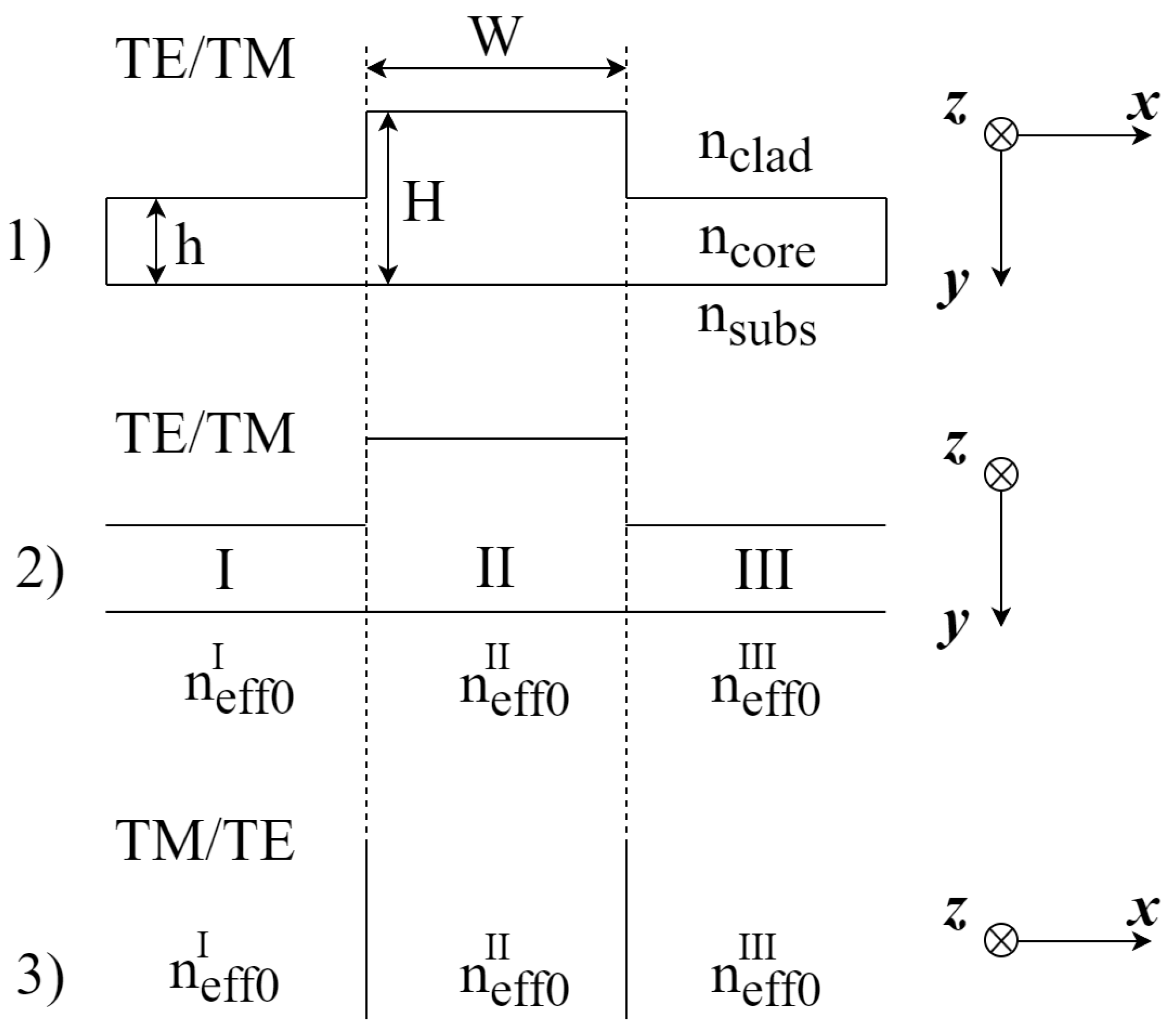
  • Then, the effective index of the fundamental mode should be calculated for each 1D waveguide (Figure 3, Step 2). This way, the effective refractive indices of the background (I and III regions) and waveguide (region II) will be calculated;
  • Next, the waveguide is presented as a planar waveguide with thickness W (Figure 3, Step 3) using the effective indices calculated in Step 2 (Figure 3, Step 3);
  • Finally, the effective index should be calculated by simulating the planar waveguide obtained in Step 3.
It should be noted that for the calculation of the effective index of the TE mode propagating in the 2D channel waveguide, firstly, TE mode analysis (Step 2) and then TM mode analysis (Steps 3–4) should be performed. For the effective index calculation of the TM mode, the steps should carried out in the following order: TM mode analysis (Step 2) and then TE mode analysis (Steps 3–4).
In cases where a deep-etched waveguide (h = 0) or planar waveguides (in regions I and III) do not guide the fundamental mode, n e f f 0 I and n e f f 0 I I I are equal to the refractive indices of n c l a d .
One of the key advantages of this method is the ability to represent the channel optical waveguide as an equivalent planar waveguide characterized by the refractive indices in the form of effective material parameters [30,31,32]. In this case, the mode field distribution in the equivalent planar waveguide can be described using the analytical Formula (8a–c):
U ( x ) = C (8a) cos u 2 ϕ exp v 2 + v x d for x < d 2 , (8b) cos u x d + ϕ for | x | d 2 , (8c) cos u 2 + ϕ exp w 2 w x d for x > d 2 .
where U ( x ) is either an electric or magnetic field and C is a normalization factor (9):
C = 2 d 1 + cos ( u 2 ϕ ) 2 ν + cos ( u ) cos ( 2 ϕ ) ν + cos ( u 2 + ϕ ) 2 w 1 2 ,
where u, ν , and w are the attenuation constants described using Equation (10):
ν = k 0 d N 2 n 2 2 , u = k 0 d n 1 2 N 2 , w = k 0 d N 2 n 0 2 ,
where k 0 is the wavenumber in vacuum, d is the thickness of the planar waveguide, N is the effective refractive index of the mode, n 1 is the refractive index of the waveguide core, n 2 is the refractive index of the substrate, n 0 is the refractive index of the cladding, and ϕ is the phase addend determined by the order and polarization of the mode (11):
ϕ = 1 2 arctan ( u w ) arctan ( ν u ) + m π for TE polarization , arctan ( n 1 2 n 2 2 w u ) arctan ( ν u ) + m π for TM polarization ,
where m is the mode order [12]. The mode decomposition coefficients a k and a j for the modes guided in the planar waveguide can be written as overlap integrals for the orthonormal modes (12):
a j k = U k ( x ) U j ( x ) d x .
The validity of Formula (12) follows from the assumption that the modes in the optical waveguide can be represented as quasi-TE and quasi-TM modes [29].
Hence, the problem of developing the analytical method to model an MMI coupler is separated into a number of sub-problems: the analytical calculation of the overlap integral for the modes propagating in the optical planar waveguide (12), described by Equations (8a–c)–(11); the derivation of the interference field (7) in the MMI box; and the analytical calculation of the overlap integrals (12) for the mode in the output waveguide and the interference field in the MMI box (at the BC plane in Figure 2). There are no restrictions on the number of modes in the MMI box or the number of input and output waveguides.

3. Results

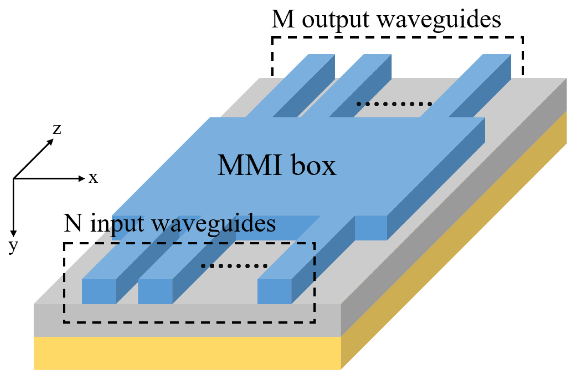
3.1. Model Building of an N × M MMI Coupler

The mode field distribution in the input or output waveguide is defined as U w g , and the mode field distribution in the MMI box is U m m i . Since the mode field distributions U w g and U m m i are piecewise-specified functions, the overlap integral (12) can be written as a sum of integrals, as expressed in (13):
a w g , m m i = D 2 U w g U m m i d x + D 2 d 2 + s U w g U m m i d x + d 2 + s d 2 + s U w g U m m i d x + + d 2 + s D 2 U w g U m m i d x + D 2 U w g U m m i d x ,
where D is the width of the MMI box, d is the width of the input or output waveguide, and s is the offset of the center of the input or output waveguide relative to the center of the MMI box along the end face (planes AF or BC in Figure 2). The first integral in Equation (13) describes the overlap of the evanescent fields at the ‘input waveguide–MMI box’ interface (AF plane in Figure 2) of the U w g and U m m i mode fields defined by Equation (8a). All constants are moved outside the integral sign, the product of the exponents is represented as an exponent of the sum of powers, and the final expression is integrated within the given limits:
I 1 = D 2 U w g U m m i d x = A 1 e x p ( D ν w g + d ν m m i 2 d ) , A 1 = C w g C m m i cos ( u w g 2 ϕ w g ) cos ( u m m i 2 ϕ m m i ) · · exp ( ν w g 2 + ν m m i 2 ν w g s d ) d D D ν w g + d ν m m i .
In cases where the input or output waveguides are located far from the edge of the MMI box (far from the AB and FC planes in Figure 2), the contribution of this integral to the total value of the overlap integral (13) is minimal. However, when the waveguide is located near the edge of the MMI box (near the AB and FC planes in Figure 2), the contribution described by Equation (14) cannot be neglected, and the larger the mode order, the larger its contribution.
The second integral in Equation (13) describes the overlap of the evanescent fields of the mode guided in the input or output waveguide and the portion of the mode guided in the MMI box, defined using Equation (8b). To calculate this integral, the method of integration by parts according to the formula u d v = u v v d u should be applied. For integration by parts, we move all constants outside the integral sign and choose the cosine as the function f and the exponent as the differential d g :
D 2 d 2 + s U w g U m m i d x = A 2 D 2 d 2 + s exp ( u w g 2 x ) cos ( u m m i D x + ϕ m m i ) d x , A 2 D 2 d 2 + s f ( x ) d g ( x ) = A 2 [ f ( x ) g ( x ) ] d 2 + s D 2 D 2 d 2 + s g ( x ) d f ( x ) , A 2 = C w g C m m i cos ( u w g 2 ϕ w g ) exp ( ν w g 2 ν w g d s ) , f ( x ) = cos ( u m m i D x + ϕ m m i ) , d g ( x ) = exp ( ν w g d x ) d x , d f ( x ) = U m m i D sin ( u m m i D x + ϕ m m i ) d x , g ( x ) = d ν w g exp ( ν w g d x ) .
Then, we can see that there is the product of the exponent and the sine function on the right side under the integral sign:
D 2 d 2 + s g ( x ) d f ( x ) = U m m i D d ν w g D 2 d 2 + s exp ( ν w g d x ) sin ( u m m i D x + ϕ m m i ) d x
Now, if we re-apply the integration by parts formula to the integral on the right side, we obtain the product f g as a product of the sine function and the exponent, and the original integral, multiplied by a constant, will be under the integral sign:
D 2 d 2 + s g ( x ) d f ( x ) = U m m i D d ν w g [ f ( x ) g ( x ) ] D 2 d 2 + s + D 2 d 2 + s g ( x ) d f ( x ) , f ( x ) = sin ( u m m i D x + ϕ m m i ) , d g ( x ) = exp ( ν w g d x ) d x , d f ( x ) = U m m i D cos ( u m m i D x + ϕ m m i ) d x , g ( x ) = d ν w g exp ( ν w g d x ) .
Then, we may carry the integral from the right side to the left, simplify the expression, and as a result, obtain the value of the original integral:
I 2 = D 2 d 2 + s U w g U m m i d x = A 2 exp ( η ( s d 2 ) η 2 + ξ 2 { η cos ( ξ [ s d 2 ] + ϕ m m i ) + + ξ sin ( ξ [ s d 2 ] + ϕ m m i ) } exp ( η ( d 2 ) ) η 2 + ξ 2 { η cos ( ξ D 2 + ϕ m m i ) + + η sin ( ξ D 2 + ϕ m m i ) }
A 2 = C w g C m m i cos u w g 2 ϕ w g exp ν w g 2 ν w g s d ,
where η = ν w g / d and ξ = u m m i / D . The third integral in (13) describes the overlap of the mode guided in the core of the input or output waveguide and the mode guided in the MMI box, defined using Equation (8b). Its integrand is the product of cosine functions, which can be represented as cos ( α ) cos ( β ) = 1 2 [ cos ( α + β ) + cos ( α β ) ] .
I 3 = d 2 + s d 2 + s U w g U m m i d x = C w g C m m i d 2 + s d 2 + s cos u w g d ( x s ) + ϕ w g cos u m m i D x + ϕ m m i d x , I 3 = C w g C m m i 2 ( I 31 + I 32 ) , I 31 = d 2 + s d 2 + s cos u w g d ( x s ) + ϕ w g + u m m i D x + ϕ m m i d x , I 32 = d 2 + s d 2 + s cos u w g d ( x s ) + ϕ w g u m m i D x ϕ m m i d x .
After rearranging the terms into I 31 and I 32 , the integrals can be obtained:
I 31 = d D D U w g + d U m m i sin D U w g + d U m m i d D x u w g d s + ϕ w g + ϕ m m i d 2 + s d 2 + s , I 32 = d D D U w g d U m m i sin D U w g d U m m i d D x u w g d s + ϕ w g ϕ m m i d 2 + s d 2 + s ,
Now, we can combine the sum of the sine functions into I 31 and I 32 and represent them as the product of the cosine and sine functions according to sin ( α ) + cos ( β ) = 2 [ sin ( ( α + β ) / 2 ) ] cos ( ( α β ) / 2 ) ] . As a result, the following equation is obtained:
I 3 = d 2 s d 2 + s U w g U m m i d x = n = 1 2 C m m i C w g d D ( 1 ) n d u m m i + D u w g · · sin ( 1 ) n d u m m i + D u w g 2 D cos ( 1 ) n ϕ w g + ϕ m m i + u m m i D s ,
The fourth integral is calculated similarly to the second one in (13):
I 4 = d 2 + s D 2 U w g U m m i d x = A 4 exp ( ζ ( s + d 2 ) ζ 2 + ξ 2 { ζ cos ( ξ [ s + d 2 ] + ϕ m m i ) ξ sin ( ξ [ s + d 2 ] + ϕ m m i ) } + exp ( ζ D 2 ) ζ 2 + ξ 2 { ξ sin ( ξ D 2 + ϕ m m i ) ζ cos ( ξ D 2 + ϕ m m i ) } ,
A 4 = C w g C m m i cos u w g 2 + ϕ w g exp w w g 2 w w g s d ,
where ζ = w w g / d . The fifth integral is calculated similarly to the first one:
I 5 = D 2 U w g U m m i d x = A 5 e x p ( D w w g + d w m m i 2 d ) , A 5 = C w g C m m i cos ( u w g 2 + ϕ w g ) cos ( u m m i 2 + ϕ m m i ) · · exp ( w w g 2 + w m m i 2 + w w g s d ) d D D w w g + d w m m i .
The propagation of radiation over the MMI box is described by Equation (6). Therefore, modes reach the output end face of the MMI box with a phase shift (determined by the length of the MMI box and the propagation constant), and their phase and amplitude are weighted by the value of the overlap integral a w g , m m i . To calculate the overlap integral between the modes propagating in the output waveguides and the field in the MMI box, the overlap integrals between each mode propagating in the MMI box and the modes propagating in the output waveguides should be calculated. Then, the forward S-parameters can be obtained as:
S i j = m m i a w g _ o u t , m m i ( a w g _ i n exp ( j β m m i L m m i ) ) ,
where summation occurs over all modes in the MMI box. a w g i n , m m i is the overlap integral of the mode in the input waveguide and the mode in the MMI box, a w g o u t , m m i is the overlap integral of the mode in the output waveguide and the mode in the MMI box, β m m i is the propagation constant of the mode in the MMI box, and L m m i is the length of the MMI box. The parameters S i j link the input port j and output port i of the MMI coupler. It should be noted that the ports i and j can represent modes of different orders and polarizations. In addition, the forward S-parameters do not consider phase differences in the input and output tapers according to the developed analytical method (phase shift of optical radiation in the input and output tapered waveguides is the same). Otherwise, the propagation of radiation within the tapers should be modeled separately.
The proposed method allows for the simulation of MMI couplers for both TE and TM polarizations. The effective indices must be calculated using the EIM for the chosen polarization. In the analytical Equations (18)–(25), the polarization defines the parameters ϕ m m i and ϕ w g according to Equation (11).

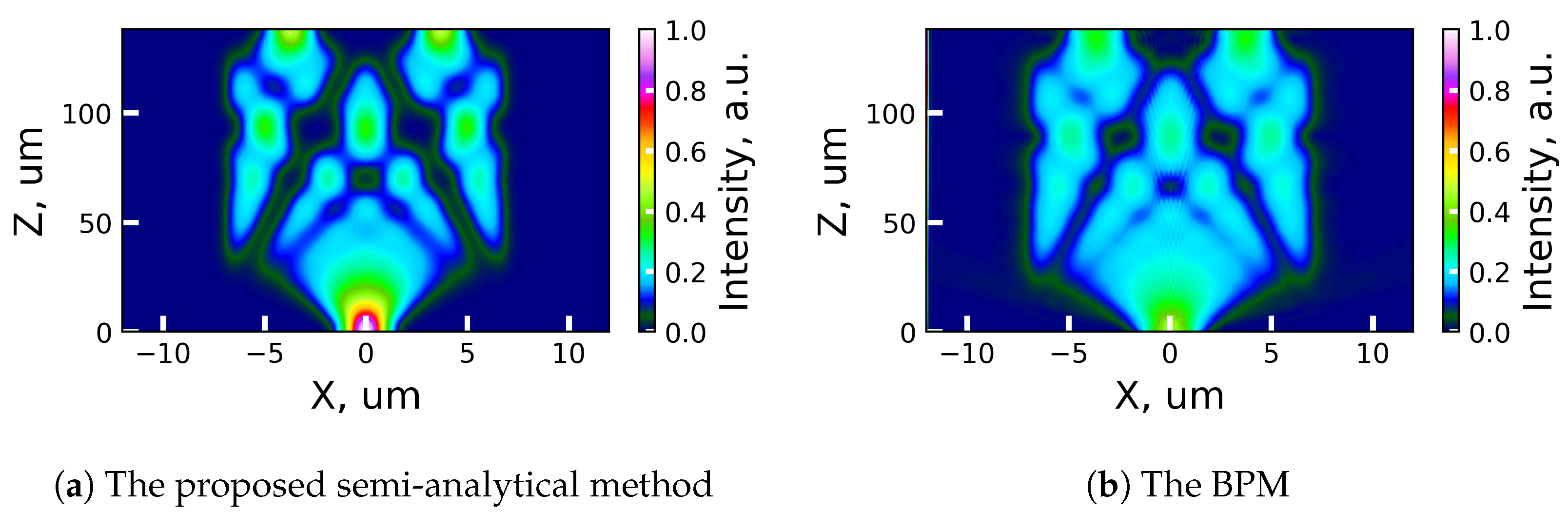
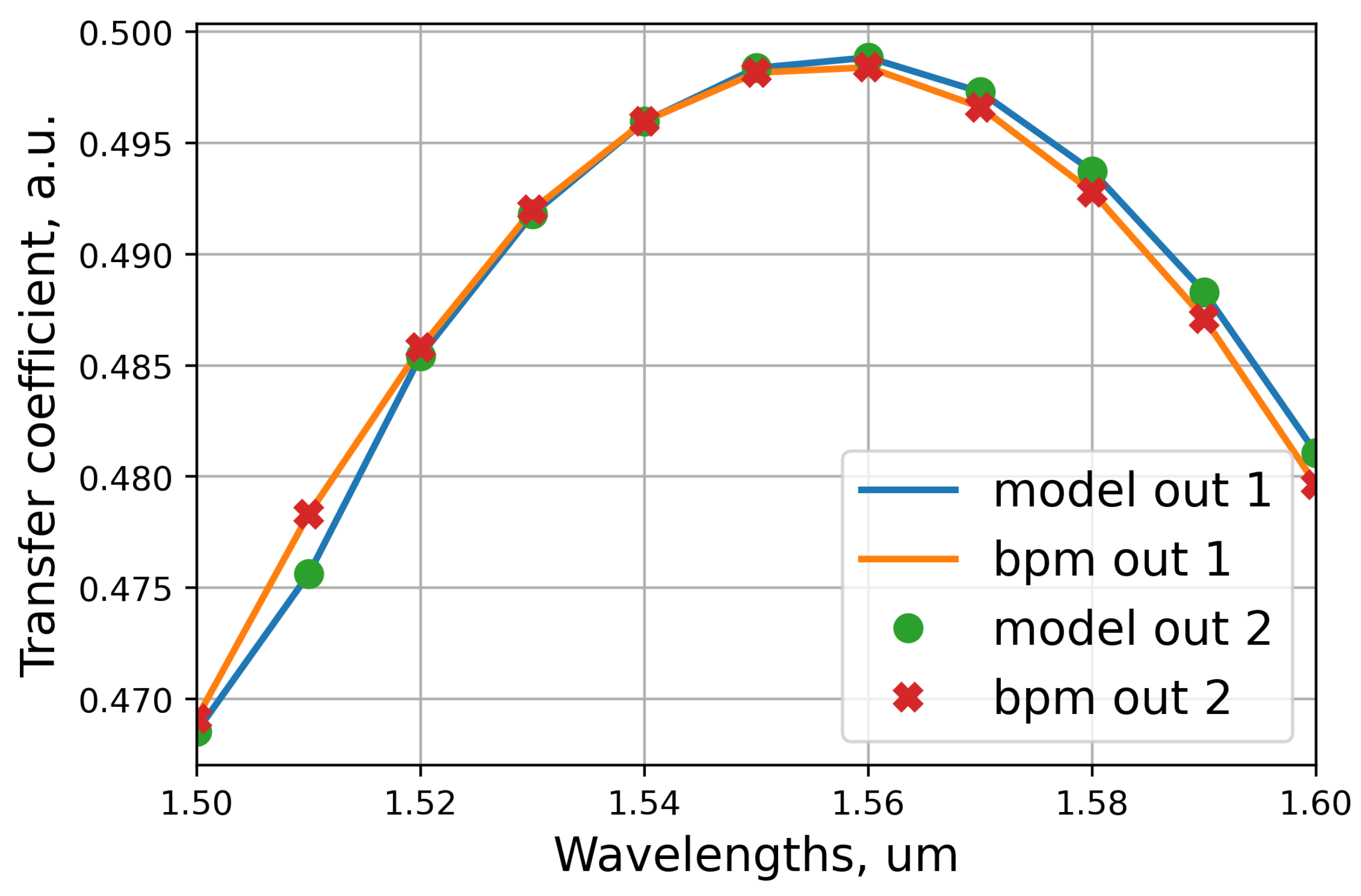
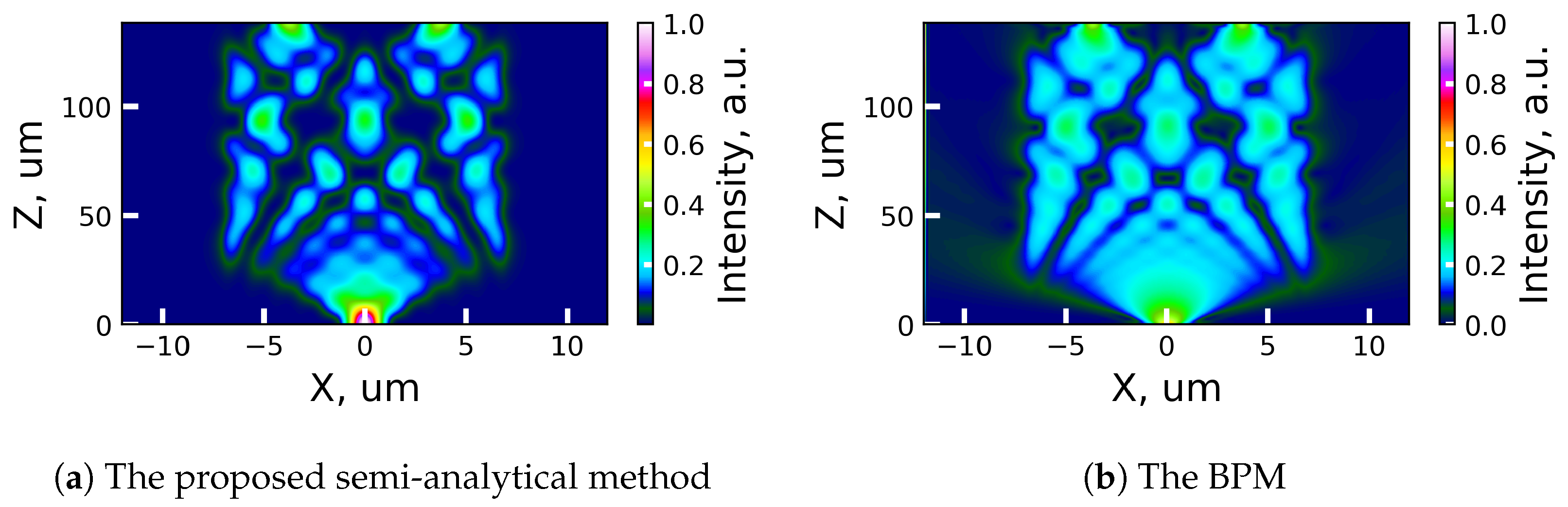
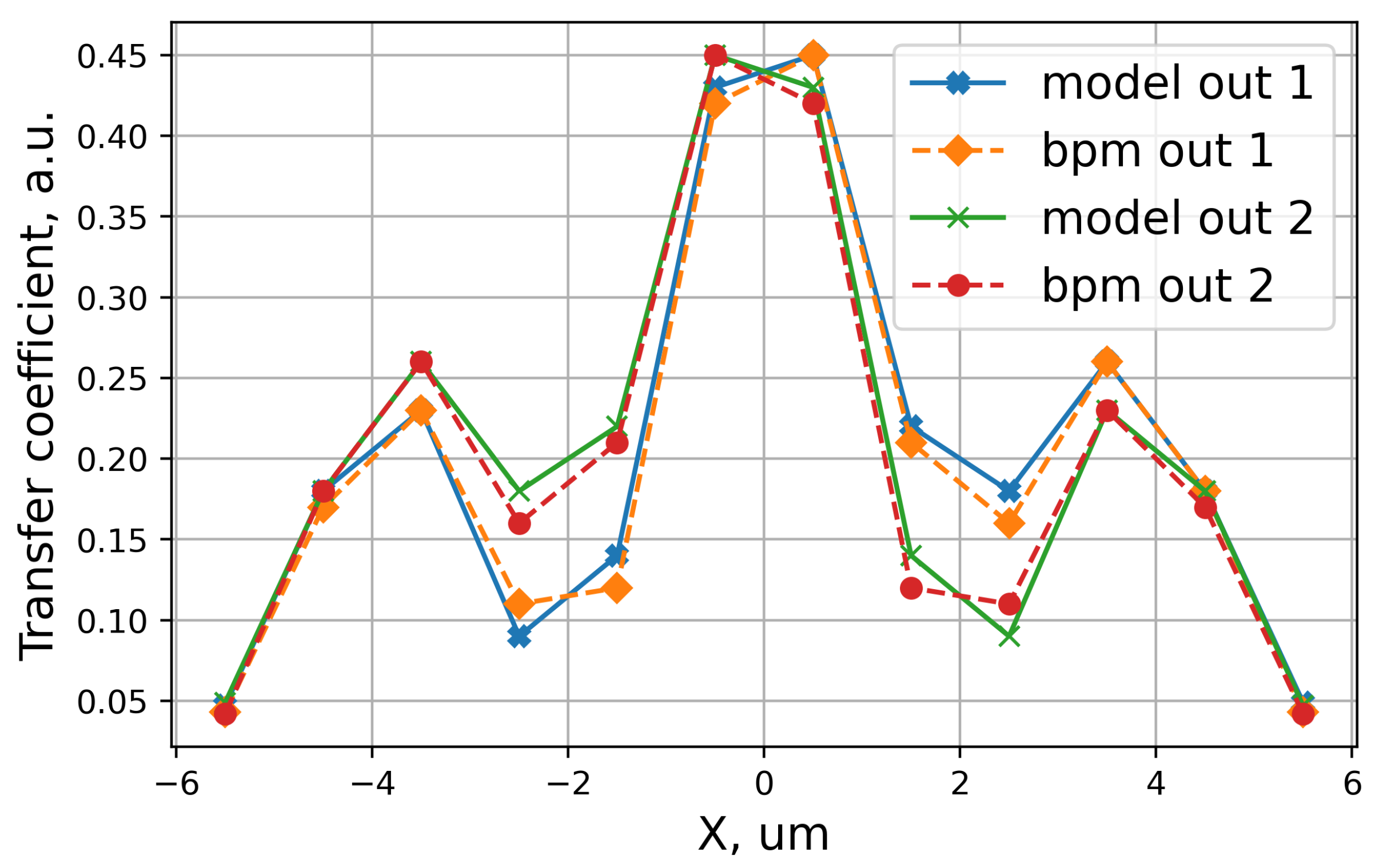
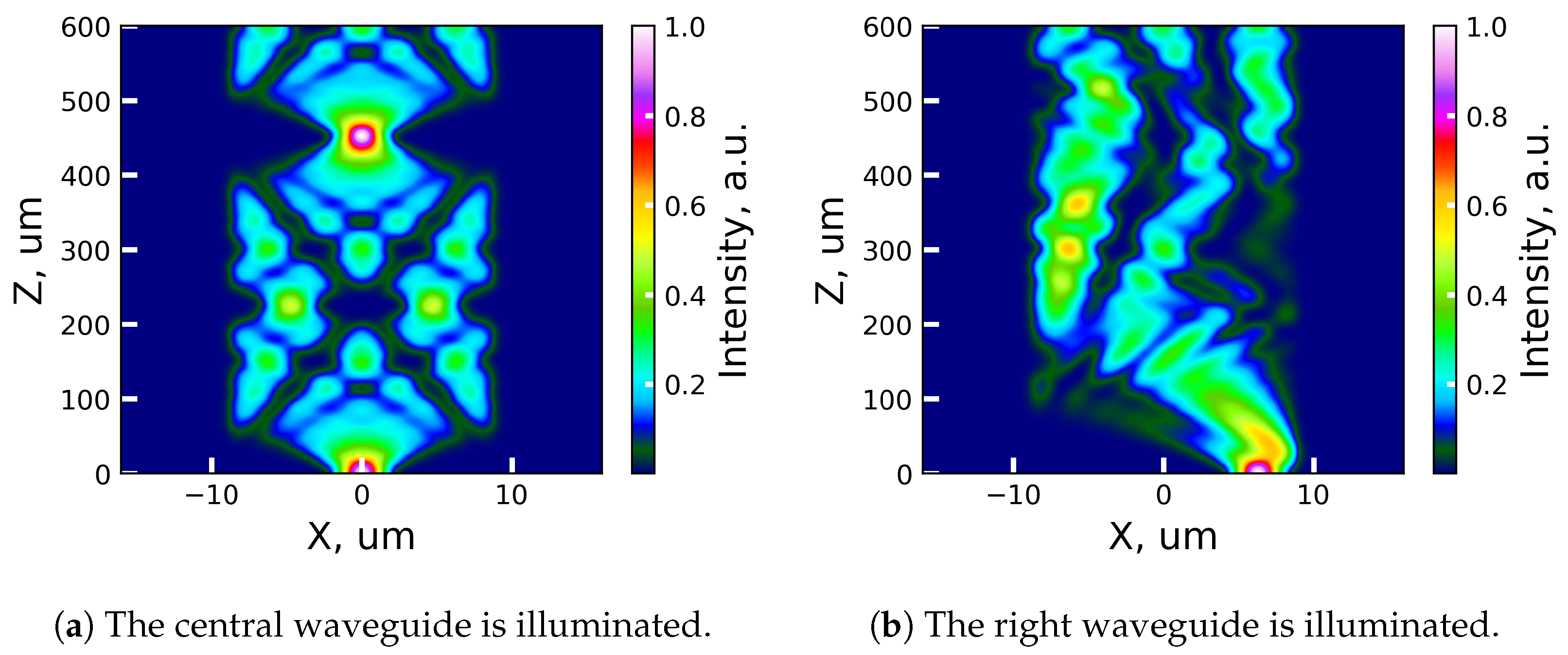
3.2. The Validation of the Proposed Semi-Analytical Method

The developed method for MMI coupler modeling and S-parameter calculations is entirely analytical, whereas the calculation of the effective indices by the EIM is semi-analytical; it enables the computation of the distribution of the electromagnetic field over the topology. No assumptions were made about the configuration of the MMI coupler or the position of the input and output waveguides in the deriving model equations, as well as about the distribution of the mode fields in the MMI box (except the assumptions made by the EIM).
For the validation of the developed analytical method, the obtained results were compared with the simulation results found using the numerical two-dimensional BPM.
The MMI coupler can be modeled using the BPM with high accuracy since this photonic building block is an extended structure, where the electromagnetic field substantially propagates along the z-axis of the MMI coupler with minimal back reflections, which is ensured by the input and output tapered waveguides. Several variations of a 1 × 2 MMI coupler based on an X-cut of thin-film lithium niobate ( T F L N ) were simulated. It was assumed that the waveguide used silicon oxide as the substrate, the thickness of the lithium niobate (LN) waveguide layer was 600 nm, and air was used as cladding. The modeling was performed using the following refractive indices of the waveguide: n L N = 2.20 , n a i r = 1.00 , and n S i O 2 = 1.45 at a wavelength of 1.55 μ m. Shallow-etched waveguides with an etching depth of 300 nm and a sidewall slope angle of 70 degrees were considered. Previously, it was shown in [33,34] that the EIM can be applied for simulating waveguides of the described configuration. The transfer coefficient of optical power from the input waveguide to the output waveguides was chosen as the main quantitative parameter characterizing the correctness of the developed semi-analytical method. This coefficient was calculated as the square of the modulus of the forward S-parameter. In addition, the similarity of the interference patterns in the MMI box obtained using the semi-analytical method and the BPM was evaluated. Using the EIM, the three-dimensional MMI coupler modeling problem was represented as an equivalent two-dimensional one through the introduction of the effective refractive indices of the waveguide and backgrounds, which were 1.95707 and 1.85367, respectively. Both values were obtained for the TE polarization of the electromagnetic field propagating in an MMI box with a width of 14 μ m. The value of the effective refractive index of the background was determined using the methods proposed in [33,35,36] to reduce the approximation error of the three-dimensional structure by applying the EIM in two dimensions.
The discretization parameters that ensured the convergence of the 2D BPM results were determined through gradual mesh densification, continuing until the change in the overlap integrals in the output waveguides did not exceed 0.001 with each densification iteration. For a computational window with a length of 240 μ m and width of 24 μ m, the discretization steps were 0.01 μ m along the x-axis and 0.1 μ m along the z-axis for the BPM calculations. As boundary conditions, a perfectly matched layer with a thickness of 1 μ m and a reflectivity of 10 6 was used for the BPM.
A 1 × 2 MMI coupler with tapered input and output waveguides was simulated using both the BPM and the proposed analytical method. This simulation was carried out to check the values of the transfer coefficients obtained through the analytical method. The topology parameters of the 1 × 2 MMI coupler were as follows: the length of the MMI box, corresponding to a 50% to 50% division, was 136 μ m; the width of the MMI box was 14 μ m; the width of the tapers was 3 μ m; the width of the input and output waveguides was 1 μ m; the length of the tapers was 25 μ m; and the distance between the centers of the output tapers was 3.68 μ m.
Both the BPM and the proposed semi-analytical method showed similar simulation results: the 1 × 2 MMI coupler with the above-described topology parameters was characterized by minimal scattering and back-reflection losses, and the values of the transfer coefficients were 0.497. The field intensity distributions over the topology of the 1 × 2 MMI coupler obtained using the BPM and the semi-analytical method also appeared similar (Figure 4):
Another crucial parameter for MMI couplers is the spectral dependence of the S-parameters. For the considered 1 × 2 MMI coupler, the S-parameters were calculated using the proposed model and the BPM for wavelengths ranging from 1.5 to 1.6 μ m (Figure 5). To properly evaluate the forward S-parameters, the EIM was applied to the optical waveguides propagating the radiation of each considered wavelength.
The accuracy of the representation of the mode field distribution over the MMI box is determined by the number of decomposition terms in Equation (5). When the proposed semi-analytical method was built, it was assumed that the guided modes should be taken into account and that the radiation modes could be ignored. To validate this assumption, the 1 × 2 MMI coupler without tapers was modeled.
In this case, the results obtained using the BPM showed the appearance of radiation modes at the output end face of the MMI box, and the values of the transfer coefficients were 0.453 in each output waveguide. Using the semi-analytical method, similar values of the transfer coefficients were obtained: 0.446 in each output waveguide. The field intensity distributions over the MMI box of the 1 × 2 MMI coupler without tapers obtained using the BPM and the semi-analytical method are shown in Figure 6. The radiation modes arising from the radiation propagation over the MMI box are demonstrated in the field intensity distribution obtained using the BPM.
As can be seen from the above results, the power fraction of the radiation modes turned out to be small: the transfer coefficients obtained using the BPM decreased by 0.044 (from 0.497 to 0.453) when the design of the MMI was made without tapers. Further, to increase the optical losses in the structure, the length of the MMI box was increased by 27 μ m (to 163 μ m). In this configuration, the resulting field reached the end of the MMI box in a mismatched form without pronounced interference maxima, so most of the power was converted into radiation modes. The field intensity distributions over the 163 μ m length MMI box are shown in Figure 7.
The transfer coefficients for the MMI coupler with a 163 μ m length MMI box obtained using the BPM and the semi-analytical method were 0.160 and 0.162, respectively. Therefore, it can be concluded that the decomposition of the resulting field into guided modes only provided a sufficiently accurate result for calculating the overlap integrals between the resulting field in the MMI box and the mode fields in the output waveguides.
However, it should be noted that in the case of the 163 μ m length MMI box, radiation modes occurred at the output of the MMI box, which may have affected the modes propagating in the output waveguides and the values of the S-parameters.
The simulation results obtained using the developed semi-analytical method were independent of the position of the input and output waveguides. This was determined by the capability to accurately calculate the overlap integrals between the modes for an arbitrary configuration (quantity and position) of the input and output waveguides and the absence of restrictions on their positions in the final formulas of the presented semi-analytical method.
However, the accuracy of the S-parameter calculations may decrease in cases where the waveguides are notably displaced relative to the optimal positions that ensure a 50% to 50% division between the output waveguides and the absence of radiation modes in the mode decomposition described by Equation (5).
To verify the independence of the calculation results from the position of the waveguides in the 1 × 2 MMI coupler, the input tapered waveguide was shifted from the lower edge of the MMI box (point F in Figure 2) to the upper one (point A in Figure 2) with a step of 1 μ m, and the transfer coefficient was calculated for each position. As can be seen in Figure 8, the difference in the values of the transfer coefficients obtained using the BPM and the developed semi-analytical method is insignificant in the absence of radiation modes. Calculations were carried out for the 138 μ m length MMI box.
Further, a 3 × 3 MMI coupler was simulated to demonstrate that the proposed method could be used for more complex MMI couplers (Figure 9). The effective refractive indices of the waveguide and the background were 1.95707 and 1.85367, respectively. The input optical radiation had a wavelength of 1.55 μ m and was TE-polarized. The length of the MMI box was 600 μ m and the width was 18 μ m. The length and width of the tapers were 50 μ m and 4.3 μ m, respectively.

4. Conclusions

A semi-analytical method for the forward S-parameter calculations of an N × M MMI coupler is proposed in this paper. This semi-analytical method allows for simulating the propagation of the optical radiation and obtaining the field intensity distribution over the MMI box, as well as calculating the overlap integrals between the guided modes in the MMI box and the input and output waveguides. The proposed semi-analytical method does not impose restrictions on the number of input and output modes or the location of the input and output waveguides. Since the developed semi-analytical method is built in terms of overlap integrals, it can be used to construct the scattering or transfer matrices of MMI couplers, which can be used to carry out circuit modeling. Also, the proposed semi-analytical method can be used to simulate the MMI tapers in AWG analytical models. The developed semi-analytical method is based on the EIM, assuming that the radiation in the waveguide is strongly polarized along the transverse axes, allowing the guided modes to be approximated by quasi-TE and quasi-TM modes. For some high-index-contrast waveguides based on silicon-on-insulator, this condition is not commonly satisfied, since in the general case, the modes guided in such channel waveguides are hybrid and the direction of electric field oscillation does not commonly coincide with the transverse axes. Mode hybridity is increased when the propagating modes are close to the cutoff, the slope angle of the waveguide sidewalls is less than 90 ° , or the waveguide material (cladding, core, or substrate) is anisotropic. However, when the modes are far from the cutoff and the waveguide is characterized by a large width-to-height ratio, the EIM works highly accurately. In practice, both the input and output waveguides, as well as the MMI box, are wide enough to ensure high accuracy of the EIM. Thus, the developed semi-analytical method has an accuracy comparable to the BPM. It allows simulation of the MMI coupler with any number and position of the input and output waveguides, and it can be used as part of circuit simulation, which can significantly increase the speed of PIC development. The developed method can be extended, for example, by adding radiation modes to the mode decomposition (5) to represent the field distribution more accurately. This can be useful in cases where the input and output waveguides do not have adiabatic tapers, i.e., their topology (width) changes rapidly, resulting in the generation of radiation modes. The mode conversion in the output waveguides can be evaluated using coupled local-mode theory. Also, the developed semi-analytical method can be extended with back-propagating modes.

Author Contributions

D.M.: methodology, development of the presented method, numerical simulation, investigation, analysis, and writing—original draft; A.K.: conceptualization and writing—review and editing; U.S.: conceptualization and writing—review and editing; V.K.: supervision and review; A.V.P.: supervision and review; V.V.: supervision and review. All authors have read and agreed to the published version of the manuscript.

Funding

This research was funded by the Ministry of Science and Higher Education of the Russian Federation (Project No. FSNM-2023-0005).

Institutional Review Board Statement

Not applicable.

Informed Consent Statement

Not applicable.

Data Availability Statement

The data reported in this manuscript are available on request from the corresponding author.

Acknowledgments

The authors would like to thank Evgenii Voblikov for the discussion about the mathematical and physical aspects of the presented results and Evgeniia Moiseeva for the valuable comments regarding the presentation of the results and the organization of the text.

Conflicts of Interest

The authors declare no conflict of interest.

Abbreviations

The following abbreviations are used in this manuscript:
MMI CouplerMultimode Interference Coupler
BPMBeam Propagation Method
PICPhotonics Integrated Circuit
FDFDFinite-Difference Frequency Domain
FDTDFinite-Difference Time Domain
FETDFinite-Element Time Domain
AWGArrayed Waveguide Grating
TE modeTransverse Electric mode
TM modeTransverse Magnetic mode
TFLNThin-Film Lithium Niobate
LNLithium Niobate
EIMEffective Index Method

References

  1. Ye, W.N.; Xiong, Y. Review of silicon photonics: History and recent advances. J. Mod. Opt. 2013, 16, 1299–1320. [Google Scholar] [CrossRef]
  2. Zhang, Y.; Schneider, M.; Karnick, D.; Eisenblätter, L.; Kühner, T.; Weber, M. Key building blocks of a silicon photonic integrated transmitter for future detector instrumentation. J. Instrum. 2019, 14, 08021. [Google Scholar] [CrossRef]
  3. Shi, Y.; Zhang, Y.; Wan, Y.; Yu, Y.; Zhang, Y.; Hu, X.; Xiao, X.; Xu, H.; Zhang, L.; Pan, B. Silicon photonics for high-capacity data communications. Photonics Res. 2022, 10, A106–A134. [Google Scholar] [CrossRef]
  4. Bogaerts, W.; Chrostowski, L. Silicon photonics circuit design: Methods, tools and challenges. Laser Photonics Rev. 2018, 12, 1700237. [Google Scholar] [CrossRef]
  5. Sullivan, D.M. Electromagnetic simulation using the FDTD method. In Electromagnetic Simulation Using the FDTD Method; John Wiley & Sons: Hoboken, NJ, USA, 2013. [Google Scholar]
  6. Rumpf, R.C. Electromagnetic and Photonic Simulation for the Beginner: Finite-Difference Frequency-Domain in MATLAB. In Electromagnetic and Photonic Simulation for the Beginner; Artech House: Norwood, MA, USA, 2022. [Google Scholar]
  7. Otin, R. ERMES: A nodal-based finite element code for electromagnetic simulations in frequency domain. Comput. Phys. Commun. 2013, 11, 2588–2595. [Google Scholar] [CrossRef]
  8. Jin, J.M. The finite element method in electromagnetics. In The Finite Element Method in Electromagnetics; John Wiley & Sons: Hoboken, NJ, USA, 2015. [Google Scholar]
  9. Melati, D.; Morichetti, F.; Canciamilla, A.; Roncelli, D.; Soares, F.M.; Bakker, A.; Melloni, A. Validation of the building-block-based approach for the design of photonic integrated circuits. J. Light. Technol. 2012, 23, 3610–3616. [Google Scholar] [CrossRef]
  10. Gallagher, D.; Design, P. Photonic CAD matures. IEEE LEOS NewsLetter, 1 February 2008; 8–14. [Google Scholar]
  11. Bahl, M.; Zhou, Y.; Scarmozzino, R.; Heller, E.; Xu, C.; Herrmann, D.; Letay, G. Accelerating Passive and Active Silicon Photonics Design using Multiple Numerical Techniques. In Proceedings of the 2018 IEEE 15th International Conference on Group IV Photonics (GFP), Cancun, Mexico, 29–31 August 2018; pp. 1–2. [Google Scholar]
  12. Kleijn, E.; Smit, M.K.; Leijtens, X.J.M. New analytical arrayed waveguide grating model. J. Light. Technol. 2013, 20, 3309–3314. [Google Scholar] [CrossRef]
  13. Capmany, J.; Muñoz, P.; Domenech, J.D.; Muriel, M.A. Apodized coupled resonator waveguides. Opt. Express 2007, 16, 10196–10206. [Google Scholar] [CrossRef]
  14. Soldano, L.B.; Pennings, E.C.M. Optical multi-mode interference devices based on self-imaging: Principles and applications. J. Light. Technol. 1995, 13, 615–627. [Google Scholar] [CrossRef]
  15. Pathak, S.; Vanslembrouck, M.; Dumon, P.; Van Thourhout, D.; Bogaerts, W. Optimized silicon AWG with flattened spectral response using an MMI aperture. J. Light. Technol. 2013, 31, 87–93. [Google Scholar] [CrossRef]
  16. Yu, J.; Mu, J.; Chen, K.; de Goede, M.; Dijkstra, M.; He, S.; García-Blanco, S.M. High-performance 90 hybrids based on MMI couplers in Si3N4 technology. Opt. Commun. 2020, 465, 125620. [Google Scholar] [CrossRef]
  17. Lu, Z.; Han, Q.; Ye, H.; Wang, S.; Xiao, F. Manufacturing Tolerance Analysis of Deep-Ridged 90 deg Hybrid Based on InP 4×4 MMI. Photonics 2020, 7, 26. [Google Scholar] [CrossRef]
  18. Lourenco, P.; Fantoni, A.; Costa, J.; Vieira, M. Lithographic mask defects analysis on an MMI 3 dB splitter. Photonics 2019, 6, 118. [Google Scholar] [CrossRef]
  19. Huang, W.P.; Xu, C.L. Simulation of three-dimensional optical waveguides by a full-vector beam propagation method. IEEE J. Quantum Electron. 1993, 10, 2639–2649. [Google Scholar] [CrossRef]
  20. Iguchi, A.; Morimoto, K.; Tsuji, Y. Bidirectional beam propagation method based on axi-symmetric full-vectorial finite element method. IEEE Photonics Technol. Lett. 2021, 14, 707–710. [Google Scholar] [CrossRef]
  21. Pedrola, G.L. Beam propagation method for design of optical waveguide devices. In Beam Propagation Method for Design of Optical Waveguide Devices; John Wiley & Sons: Hoboken, NJ, USA, 2015. [Google Scholar]
  22. Herrero-Bermello, A.; Luque-Gonz’alez, J.M.; Velasco, A.V.; Ortega-Monux, A.; Cheben, P.; Halir, R. Design of a broadband polarization splitter based on anisotropy-engineered tilted subwavelength gratings. IEEE Photonics J. 2019, 11, 1–8. [Google Scholar] [CrossRef]
  23. Meng, Y.; Liu, Z.; Xie, Z.; Wang, R.; Qi, T.; Hu, F.; Kim, H.; Xiao, Q.; Fu, X.; Wu, Q.; et al. Versatile on-chip light coupling and (de)multiplexing from arbitrary polarizations to controlled waveguide modes using an integrated dielectric metasurface. Photonics Res. 2020, 8, 564–576. [Google Scholar] [CrossRef]
  24. Meng, Y.; Chen, Y.; Lu, L.; Ding, Y.; Cusano, A.; Fan, J.A.; Hu, Q.; Wang, K.; Xie, Z.; Liu, Z.; et al. Optical meta-waveguides for integrated photonics and beyond. Light. Sci. Appl. 2021, 10, 235. [Google Scholar] [CrossRef]
  25. Chang, W.; Ren, X.; Ao, Y.; Lu, L.; Cheng, M.; Deng, L.; Liu, D.; Zhang, M. Inverse design and demonstration of an ultracompact broadband dual-mode 3 dB power splitter. Opt. Express 2018, 26, 24135–24144. [Google Scholar] [CrossRef]
  26. Hosseini, A.; Kwong, D.; Chen, R.T. Analytical formula for output phase of symmetrically excited one-to-N multimode interference coupler. In Proceedings of the Optoelectronic Interconnects and Component Integration IX, SPIE, San Francisco, CA, USA, 23–28 January 2010; Volume 7607, pp. 381–392. [Google Scholar]
  27. Cooney, K.; Peters, F.H. Analysis of multimode interferometers. Opt. Express 2016, 20, 22481–22515. [Google Scholar] [CrossRef]
  28. Heaton, J.M.; Jenkins, R.M. General matrix theory of self-imaging in multimode interference (MMI) couplers. IEEE Photonics Technol. Lett. 1999, 11, 212–214. [Google Scholar] [CrossRef]
  29. Snyder, A.W.; Love, J.D. Optical Waveguide Theory; Chapman and Hall: London, UK, 1983. [Google Scholar]
  30. Chiang, K.S. Dual effective-index method for the analysis of rectangular dielectric waveguides. Appl. Opt. 1986, 13, 2169–2174. [Google Scholar] [CrossRef] [PubMed]
  31. Hammer, M.; Ivanova, O.V. Effective index approximations of photonic crystal slabs: A 2-to-1-D assessment. Opt. Quantum Electron. 2009, 41, 267–283. [Google Scholar] [CrossRef]
  32. Ivanova, O.V.; Stoffer, R.; Kauppinen, L.; Hammer, M. Variational effective index method for 3D vectorial scattering problems in photonics: TE polarization. In Proceedings of the Progress in Electromagnetics Research Symposium PIERS 2009, Moscow, Russia, 18–21 August 2009; pp. 1038–1042. [Google Scholar]
  33. Moskalev, D.; Kozlov, A.; Salgaeva, U.; Krishtop, V.; Volyntsev, A. Applicability of the Effective Index Method for the Simulation of X-Cut LiNbO3 waveguides. Appl. Sci. 2023, 11, 6374. [Google Scholar] [CrossRef]
  34. Kozlov, A.; Moskalev, D.; Salgaeva, U.; Bulatova, A.; Krishtop, V.; Volyntsev, A.; Syuy, A. Reactive Ion Etching of X-Cut LiNbO3 in an ICP/TCP System for the Fabrication of an Optical Ridge Waveguide. Appl. Sci. 2023, 13, 2097. [Google Scholar] [CrossRef]
  35. Wang, Q.; Farrell, G.; Freir, T. Effective index method for planar lightwave circuits containing directional couplers. Opt. Commun. 2006, 1, 133–136. [Google Scholar] [CrossRef]
  36. Han, Y.T.; Shin, J.U.; Kim, D.J.; Park, S.H.; Park, Y.J.; Sung, H.K. A rigorous 2D approximation technique for 3D waveguide structures for BPM calculations. Etri J. 2003, 6, 535–537. [Google Scholar] [CrossRef]
Figure 1. A schematic image of an N × M MMI coupler.
Photonics 10 01260 g001
Figure 2. A schematic image of an MMI coupler, 1 × 2.
Photonics 10 01260 g002
Figure 3. The effective index method algorithm.
Photonics 10 01260 g003
Figure 4. The field intensity distributions over the MMI box of the 1 × 2 MMI coupler with the tapered waveguides.
Photonics 10 01260 g004
Figure 5. The spectral dependence of the transfer coefficients.
Photonics 10 01260 g005
Figure 6. The field intensity distributions over the MMI box of the 1 × 2 MMI coupler without tapers.
Photonics 10 01260 g006
Figure 7. The field intensity distributions over the 163 μ m length MMI box of the 1 × 2 MMI coupler.
Photonics 10 01260 g007
Figure 8. The dependence of the transfer coefficients from the offset of the input waveguide.
Photonics 10 01260 g008
Figure 9. The field intensity distributions over the 600 μ m length MMI box of the 3 × 3 MMI coupler.
Photonics 10 01260 g009
Disclaimer/Publisher’s Note: The statements, opinions and data contained in all publications are solely those of the individual author(s) and contributor(s) and not of MDPI and/or the editor(s). MDPI and/or the editor(s) disclaim responsibility for any injury to people or property resulting from any ideas, methods, instructions or products referred to in the content.

