
A Review of Data Mining Applications in Semiconductor Manufacturing


Abstract
1. Introduction
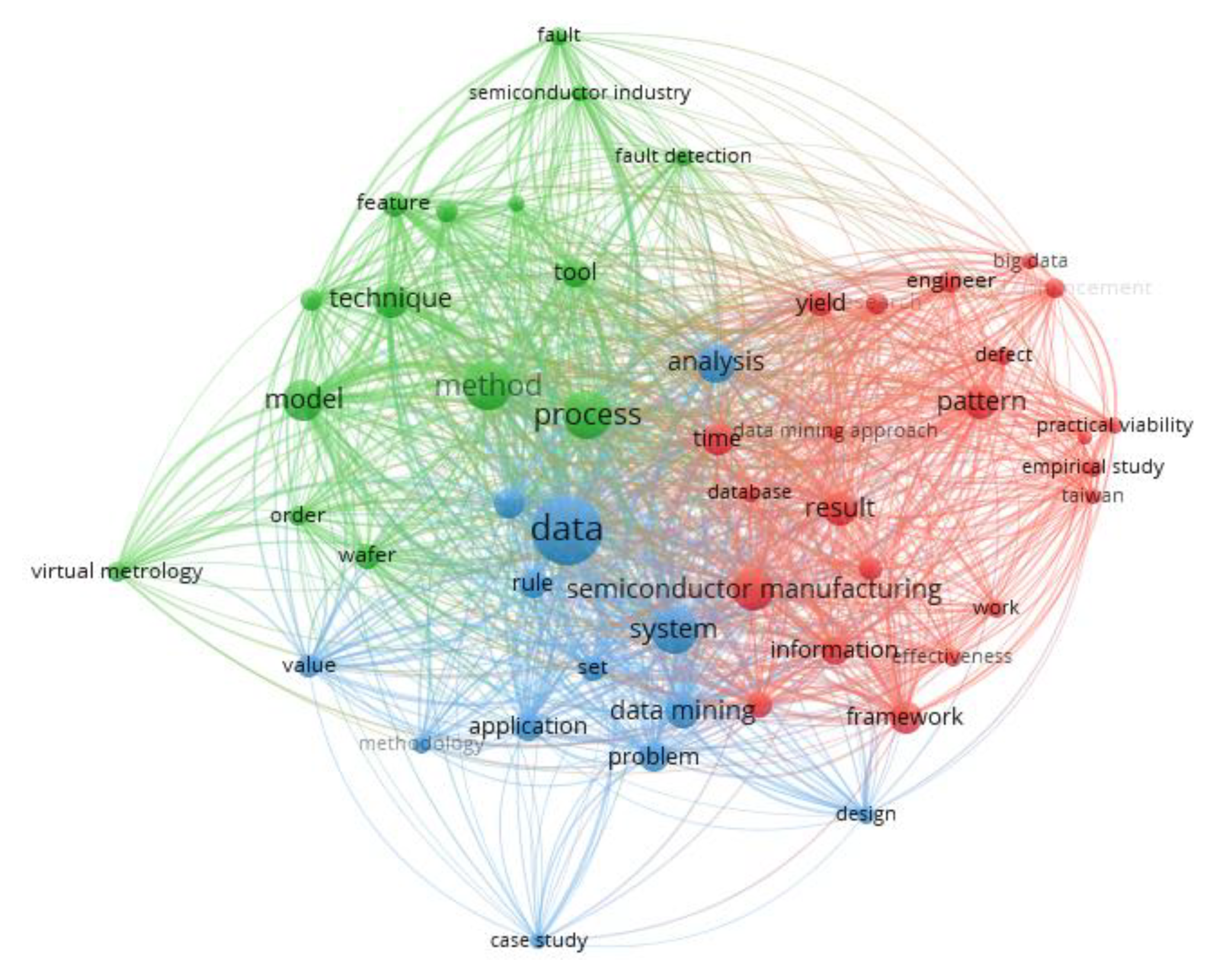
2. Bibliometric Analysis
Keyword Analysis
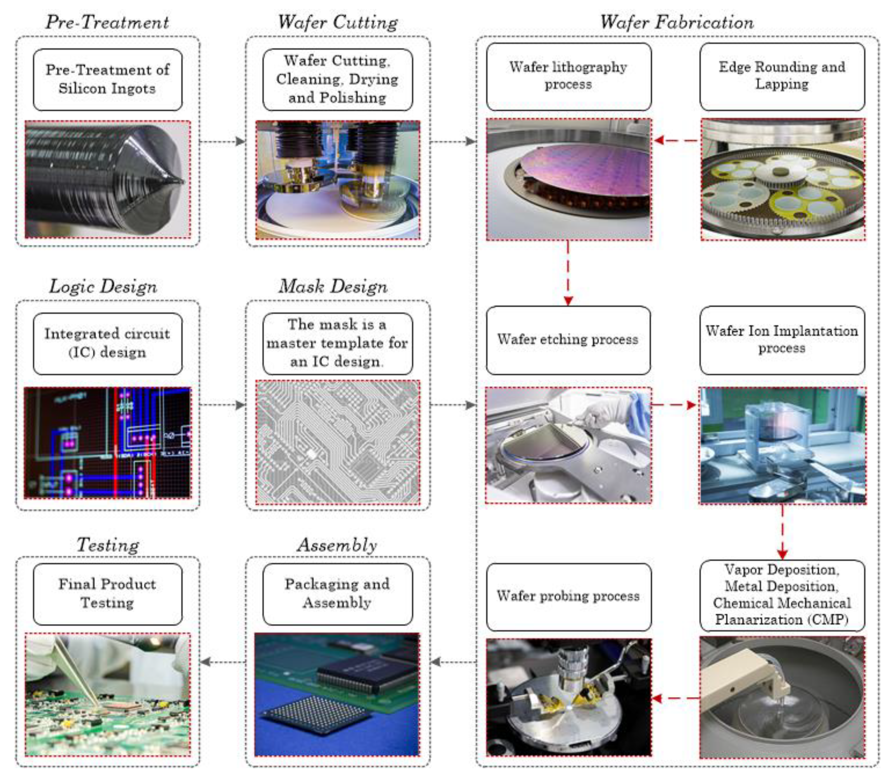
3. Semiconductor Manufacturing Process
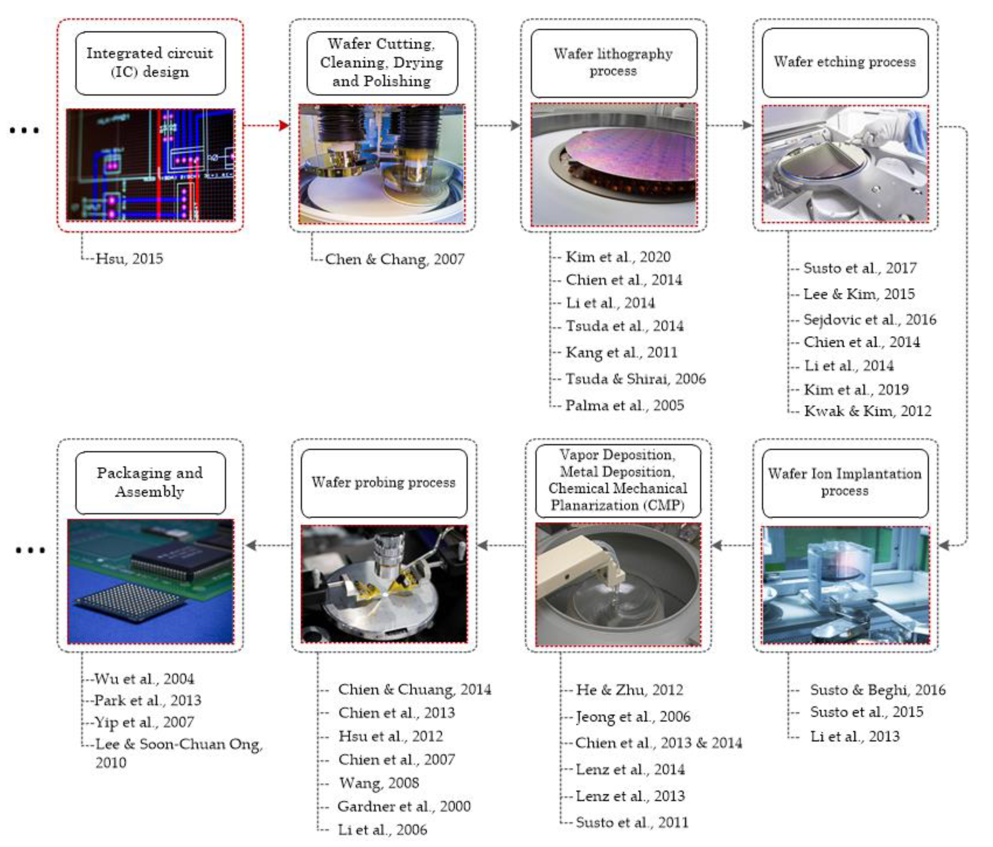
4. Data Mining Applications in Semiconductor Manufacturing
4.1. Data Mining Applications for Quality Control
4.2. Data Mining Applications for Maintenance
4.3. Data Mining Applications for Metrology, Measurement, and Instrumentation
4.4. Decision Support Systems
4.5. Data Mining Applications for Production and Production Scheduling
5. Discussion
Limitations and Challenges
- Data mining systems can violate privacy. Absence of safety and security can be very detrimental to its users and it can create miscommunication between employees, thus leading to genuine privacy concerns [177].
- Security is an important factor related to every data-oriented technology, and semiconductor manufacturing is not an exception. Data that is very critical might be a target of malicious attacks [178].
- There is a possibility of information misuse through the mining process. Data mining system have to evolve in order to diminish the misuse of the information ratio [181].
- Accuracy of data mining techniques is another limitation [182]. Accuracy is an evaluation system of measurement on how well a data mining model can perform. Many common accuracy and error scores for regression and classification can occur. Therefore, improving accuracy becomes paramount.
- Missing and imbalanced data is a challenge in this industry. In cases in which data is imbalanced, the majority of classification algorithms have as a consequence a weak performance. Since wafer yield enhancement is a crucial performance index in semiconductor wafer manufacturing, key process steps must be cautiously selected and managed [9].
- Data processing time is another limitation that has a significant impact on the available time since data preprocessing very often involves more than 50% of time and effort of the entire data analysis process [185].
6. Conclusions
Author Contributions
Funding
Institutional Review Board Statement
Informed Consent Statement
Data Availability Statement
Conflicts of Interest
References
- Biebl, F.; Glawar, R.; Jalali, A.; Ansari, F.; Haslhofer, B.; de Boer, P.; Sihn, W. A Conceptual Model to Enable Prescriptive Maintenance for Etching Equipment in Semiconductor Manufacturing. Proc. CIRP 2020, 88, 64–69. [Google Scholar] [CrossRef]
- Bui, P.-D.; Lee, C. Unified System Network Architecture: Flexible and Area-Efficient NoC Architecture with Multiple Ports and Cores. Electronics 2020, 9, 1316. [Google Scholar] [CrossRef]
- Weber, A. Smart manufacturing in the semiconductor industry: An evolving nexus of business drivers, technologies, and standards. In Smart Manufacturing; Soroush, M., Baldea, M., Edgar, T.F., Eds.; Elsevier: Amsterdam, The Netherlands, 2020; Chapter 3; pp. 59–105. ISBN 978-0-12-820028-5. [Google Scholar]
- Hurtarte, J.S.; Wolsheimer, E.A.; Tafoya, L.M. Semiconductor Manufacturing Basics. In Understanding Fabless IC Technology; Newnes: Burlington, MA, USA, 2007; Chapter 4; pp. 41–45. ISBN 978-0-7506-7944-2. [Google Scholar]
- Khakifirooz, M.; Chien, C.F.; Chen, Y.-J. Bayesian Inference for Mining Semiconductor Manufacturing Big Data for Yield Enhancement and Smart Production to Empower Industry 4.0. Appl. Soft Comput. 2018, 68, 990–999. [Google Scholar] [CrossRef]
- Reis, M.S.; Gins, G. Industrial Process Monitoring in the Big Data/Industry 4.0 Era: From Detection, to Diagnosis, to Prognosis. Processes 2017, 5, 35. [Google Scholar] [CrossRef]
- Lin, Y.-C.; Yeh, C.-C.; Chen, W.-H.; Hsu, K.-Y. Implementation Criteria for Intelligent Systems in Motor Production Line Process Management. Processes 2020, 8, 537. [Google Scholar] [CrossRef]
- Chen, T. Strengthening the Competitiveness and Sustainability of a Semiconductor Manufacturer with Cloud Manufacturing. Sustainability 2014, 6, 251–266. [Google Scholar] [CrossRef]
- Lee, D.-H.; Yang, J.-K.; Lee, C.-H.; Kim, K.-J. A Data-Driven Approach to Selection of Critical Process Steps in the Semiconductor Manufacturing Process Considering Missing and Imbalanced Data. J. Manuf. Syst. 2019, 52, 146–156. [Google Scholar] [CrossRef]
- Hsu, C.-Y.; Chen, W.-J.; Chien, J.-C. Similarity Matching of Wafer Bin Maps for Manufacturing Intelligence to Empower Industry 3.5 for Semiconductor Manufacturing. Comput. Ind. Eng. 2020, 142, 106358. [Google Scholar] [CrossRef]
- Nakata, K.; Orihara, R.; Mizuoka, Y.; Takagi, K. A Comprehensive Big-Data-Based Monitoring System for Yield Enhancement in Semiconductor Manufacturing. IEEE Trans. Semicond. Manuf. 2017, 30, 339–344. [Google Scholar] [CrossRef]
- Yang, X.-S. Data mining techniques. In Introduction to Algorithms for Data Mining and Machine Learning; Academic Press: London, UK, 2019; Chapter 6; pp. 109–128. ISBN 978-0-12-817216-2. [Google Scholar]
- Chien, C.-F.; Wang, W.-C.; Cheng, J.-C. Data Mining for Yield Enhancement in Semiconductor Manufacturing and an Empirical Study. Expert Syst. Appl. 2007, 33, 192–198. [Google Scholar] [CrossRef]
- He, J.; Zhu, Y. Hierarchical Multi-Task Learning with Application to Wafer Quality Prediction. In Proceedings of the 2012 IEEE 12th International Conference on Data Mining, Brussels, Belgium, 10–13 December 2012; pp. 290–298. [Google Scholar]
- Jeong, M.K.; Lu, J.-C.; Huo, X.; Vidakovic, B.; Chen, D. Wavelet-Based Data Reduction Techniques for Process Fault Detection. Technometrics 2006, 48, 26–40. [Google Scholar] [CrossRef]
- Susto, G.A.; Beghi, A. Dealing with Time-Series Data in Predictive Maintenance Problems. In Proceedings of the 2016 IEEE 21st International Conference on Emerging Technologies and Factory Automation (ETFA), Berlin, Germany, 6–9 September 2016; pp. 1–4. [Google Scholar]
- Choi, J.; Jeong, M.K. Deep Autoencoder With Clipping Fusion Regularization on Multistep Process Signals for Virtual Metrology. IEEE Sens. Lett. 2019, 3, 1–4. [Google Scholar] [CrossRef]
- Wenjing, W.; Yumin, M.; Fei, Q.; Xiang, G. Data Mining Based Dynamic Scheduling Approach for Semiconductor Manufacturing System. In Proceedings of the 2015 34th Chinese Control Conference (CCC), Hangzhou, China, 28–30 July 2015; pp. 2603–2608. [Google Scholar]
- Khemiri, A.; Amine Hamri, M.E.; Frydman, C.; Pinaton, J. Improving Business Process in Semiconductor Manufacturing by Discovering Business Rules. In Proceedings of the 2018 Winter Simulation Conference (WSC ‘18), Gothenburg, Sweden, 9–12 December 2018; pp. 3441–3448. [Google Scholar]
- Huang, C.-Y.; Lin, P.K.P. Application of Integrated Data Mining Techniques in Stock Market Forecasting. Cogent Econ. Financ. 2014, 2, 929505. [Google Scholar] [CrossRef]
- Tranfield, D.; Denyer, D.; Smart, P. Towards a Methodology for Developing Evidence-Informed Management Knowledge by Means of Systematic Review. Br. J. Manag. 2003, 14, 207–222. [Google Scholar] [CrossRef]
- Denyer, D.; Tranfield, D. Producing a systematic review. In The Sage Handbook of Organizational Research Methods; Buchanan, D., Bryman, A., Eds.; Sage Publications Ltd.: London, UK, 2009; pp. 671–689. [Google Scholar]
- Rousseau, D.M.; Manning, J.; Denyer, D. Evidence in Management and Organizational Science: Assembling the Field’s Full Weight of Scientific Knowledge Through Syntheses. Acad. Manag. Ann. 2008, 2, 475–515. [Google Scholar] [CrossRef]
- Correia, E.; Carvalho, H.; Azevedo, S.G.; Govindan, K. Maturity Models in Supply Chain Sustainability: A Systematic Literature Review. Sustainability 2017, 9, 64. [Google Scholar] [CrossRef]
- Wang, K. Applying Data Mining to Manufacturing: The Nature and Implications. J. Intell. Manuf. 2007, 18, 487–495. [Google Scholar] [CrossRef]
- Harding, J.A.; Shahbaz, M.; Kusiak, A. Data Mining in Manufacturing: A Review. J. Manuf. Sci. Eng. 2006, 128, 969–976. [Google Scholar] [CrossRef]
- Buchanan, P.D.; Bryman, P.A. The Sage Handbook of Organizational Research Methods; Sage Publications Ltd.: London, UK, 2009; ISBN 978-1-4462-4605-4. [Google Scholar]
- Yan, H.; Yang, N.; Peng, Y.; Ren, Y. Data Mining in the Construction Industry: Present Status, Opportunities, and Future Trends. Autom. Constr. 2020, 119, 103331. [Google Scholar] [CrossRef]
- Galati, F.; Bigliardi, B. Industry 4.0: Emerging Themes and Future Research Avenues Using a Text Mining Approach. Comput. Ind. 2019, 109, 100–113. [Google Scholar] [CrossRef]
- Susto, G.A.; Schirru, A.; Pampuri, S.; McLoone, S.; Beghi, A. Machine Learning for Predictive Maintenance: A Multiple Classifier Approach. IEEE Trans. Ind. Inform. 2015, 11, 812–820. [Google Scholar] [CrossRef]
- Famili, A.; Shen, W.-M.; Weber, R.; Simoudis, E. Data Preprocessing and Intelligent Data Analysis. IDA 1997, 1, 3–23. [Google Scholar] [CrossRef]
- Kusiak, A. Rough Set Theory: A Data Mining Tool for Semiconductor Manufacturing. IEEE Trans. Electron. Packag. Manufact. 2001, 24, 44–50. [Google Scholar] [CrossRef]
- Kumar, S.; Sharma, P.; Garg, K.C. Lotka’s Law and Institutional Productivity. Inf. Process. Manag. 1998, 34, 775–783. [Google Scholar] [CrossRef]
- Hsu, S.-C.; Chien, C.-F. Hybrid Data Mining Approach for Pattern Extraction from Wafer Bin Map to Improve Yield in Semiconductor Manufacturing. Int. J. Prod. Econ. 2007, 107, 88–103. [Google Scholar] [CrossRef]
- Van Eck, N.J.; Waltman, L. Software Survey: VOSviewer, a Computer Program for Bibliometric Mapping. Scientometrics 2010, 84, 523–538. [Google Scholar] [CrossRef]
- Muñoz, J.A.M.; Viedma, E.H.; Espejo, A.L.S.; Cobo, M.J. Software Tools for Conducting Bibliometric Analysis in Science: An up-to-Date Review. Prof. Inf. 2020, 29, 4. [Google Scholar]
- Sordan, J.E.; Oprime, P.C.; Pimenta, M.L.; Chiabert, P.; Lombardi, F. Lean Six Sigma in Manufacturing Process: A Bibliometric Study and Research Agenda. TQM J. 2020, 32, 381–399. [Google Scholar] [CrossRef]
- Wellmann, P.J. Power Electronic Semiconductor Materials for Automotive and Energy Saving Applications—SiC, GaN, Ga2O3, and Diamond. Z. Anorg. Allg. Chem. 2017, 643, 1312–1322. [Google Scholar] [CrossRef]
- Garlapati, S.K.; Divya, M.; Breitung, B.; Kruk, R.; Hahn, H.; Dasgupta, S. Printed Electronics Based on Inorganic Semiconductors: From Processes and Materials to Devices. Adv. Mater. 2018, 30, 1707600. [Google Scholar] [CrossRef]
- Satpathy, R.; Pamuru, V. Silicon wafer manufacturing process. In Solar PV Power; Satpathy, R., Pamuru, V., Eds.; Academic Press: London, UK, 2021; Chapter 3; pp. 53–70. ISBN 978-0-12-817626-9. [Google Scholar]
- Möller, H.J. Wafering of Silicon. In Semiconductors and Semimetals; Willeke, G.P., Weber, E.R., Eds.; Elsevier: Amsterdam, The Netherlands, 2015; Volume 92, Chapter 2; pp. 63–109. [Google Scholar]
- Geng, N.; Jiang, Z. Capacity Planning for Semiconductor Wafer Fabrication with Uncertain Demand and Capacity. In Proceedings of the 2007 IEEE International Conference on Automation Science and Engineering, Scottsdale, AZ, USA, 22–25 September 2007; pp. 100–105. [Google Scholar]
- Satpathy, R.; Pamuru, V. Silicon crystal growth process. In Solar PV Power; Satpathy, R., Pamuru, V., Eds.; Academic Press: London, UK, 2021; Chapter 2; pp. 31–52. ISBN 978-0-12-817626-9. Available online: https://doi.org/10.1016/B978-0-12-817626-9.00002-2 (accessed on 2 February 2021).
- Tilli, M. Silicon wafers preparation and properties. In Handbook of Silicon Based MEMS Materials and Technologies, 3rd ed.; Tilli, M., Paulasto-Krockel, M., Petzold, M., Theuss, H., Motooka, T., Lindroos, V., Eds.; Elsevier: Amsterdam, The Netherlands, 2020; Chapter 4; pp. 93–110. ISBN 978-0-12-817786-0. [Google Scholar]
- Gallagher, E.; Hibbs, M. Masks for micro- and nanolithography. In Nanolithography; Feldman, M., Ed.; Woodhead Publishing: Cambridge, UK, 2014; Chapter 5; pp. 158–178. ISBN 978-0-85709-500-8. [Google Scholar]
- Cadien, K.C.; Nolan, L. Chapter 10—Chemical Mechanical Polishing Method and Practice. In Handbook of Thin Film Deposition, 4th ed.; Seshan, K., Schepis, D., Eds.; William Andrew Publishing: Norwich, NY, USA, 2018; pp. 317–357. ISBN 978-0-12-812311-9. [Google Scholar]
- Bao, H.; Chen, L.; Ren, B. A Study on the Pattern Effects of Chemical Mechanical Planarization with CNN-Based Models. Electronics 2020, 9, 1158. [Google Scholar] [CrossRef]
- Zhang, Y.; Wagner, L.; Golbutsov, P. Importance of Wafer Flatness for CMP and Lithography. In Proceedings of the Metrology, Inspection, and Process Control for Microlithography XI, Santa Clara, CA, USA, 7 July 1997; International Society for Optics and Photonics, 1997; Volume 3050, pp. 266–269. Available online: https://doi.org/10.1117/12.275916 (accessed on 2 February 2021).
- Ki, M.; Sungmin, K.; Taesung, K. Study on Effect of Back-Surface Treatment of Silicon Wafer in Photo Lithography Process after CMP Process. In Proceedings of the 2015 International Conference on Planarization/CMP Technology (ICPT), Chandler, AZ, USA, 30 September–2 October 2015; pp. 1–3. [Google Scholar]
- Jain, A. Ion Implantation for Semiconductor Processing. Radiat. Eff. 1982, 63, 39–46. [Google Scholar] [CrossRef]
- Zolper, J.C. Ion Implantation in Wide Bandgap Semiconductors. In Processing of Wide Band Gap Semiconductors; Pearton, S.J., Ed.; William Andrew Publishing: Norwich, NY, USA, 2000; Chapter 7; pp. 300–353. ISBN 978-0-8155-1439-8. [Google Scholar]
- Rice, B.J. Extreme ultraviolet (EUV) lithography. In Nanolithography; Feldman, M., Ed.; Woodhead Publishing: Cambridge, UK, 2014; Chapter 2; pp. 42–79. ISBN 978-0-85709-500-8. [Google Scholar]
- Marconi, M.C.; Wachulak, P.W. Extreme Ultraviolet Lithography with Table Top Lasers. Prog. Quantum Electron. 2010, 34, 173–190. [Google Scholar] [CrossRef]
- Buitrago, E.; Kulmala, T.S.; Fallica, R.; Ekinci, Y. EUV lithography process challenges. In Frontiers of Nanoscience; Robinson, A., Lawson, R., Eds.; Materials and Processes for Next Generation Lithography; Elsevier: Amsterdam, The Netherlands, 2016; Chapter 4; Volume 11, pp. 135–176. [Google Scholar]
- Kolasinski, K.W. Growth and Etching of Semiconductors. In Handbook of Surface Science; Hasselbrink, E., Lundqvist, B.I., Eds.; Dynamics; North-Holland: Amsterdam, The Netherlands, 2008; Chapter 16; Volume 3, pp. 787–870. Available online: https://doi.org/10.1016/S1573-4331(08)00016-4 (accessed on 2 February 2021).
- Chang, H.-Y.; Pan, W.-F.; Shih, M.-K.; Lai, Y.-S. Geometric Design for Ultra-Long Needle Probe Card for Digital Light Processing Wafer Testing. Microelectron. Reliab. 2010, 50, 556–563. [Google Scholar] [CrossRef]
- Sakamaki, R.; Horibe, M. Realization of Accurate On-Wafer Measurement Using Precision Probing Technique at Millimeter-Wave Frequency. IEEE Trans. Instrum. Meas. 2018, 67, 1940–1945. [Google Scholar] [CrossRef]
- Sakamaki, R.; Horibe, M. Uncertainty Analysis Method Including Influence of Probe Alignment on On-Wafer Calibration Process. IEEE Trans. Instrum. Meas. 2019, 68, 1748–1755. [Google Scholar] [CrossRef]
- Kuo, C.-H.; Hu, A.H.; Hung, L.H.; Yang, K.-T.; Wu, C.-H. Life Cycle Impact Assessment of Semiconductor Packaging Technologies with Emphasis on Ball Grid Array. J. Clean. Prod. 2020, 276, 124301. [Google Scholar] [CrossRef]
- Elshabini, A.A.; Barlow, F.; Wang, P.J. Electronic Packaging: Semiconductor Packages. In Reference Module in Materials Science and Materials Engineering; Elsevier: Amsterdam, The Netherlands, 2017; ISBN 978-0-12-803581-8. [Google Scholar]
- Sang, H.-Y.; Duan, P.-Y.; Li, J.-Q. An Effective Invasive Weed Optimization Algorithm for Scheduling Semiconductor Final Testing Problem. Swarm Evol. Comput. 2018, 38, 42–53. [Google Scholar] [CrossRef]
- Chien, C.; Chen, L. Using Rough Set Theory to Recruit and Retain High-Potential Talents for Semiconductor Manufacturing. IEEE Trans. Semicond. Manuf. 2007, 20, 528–541. [Google Scholar] [CrossRef]
- Geum, Y.; Jeon, J.; Seol, H. Identifying Technological Opportunities Using the Novelty Detection Technique: A Case of Laser Technology in Semiconductor Manufacturing. Technol. Anal. Strateg. Manag. 2013, 25, 1–22. [Google Scholar] [CrossRef]
- Tirkel, I. Forecasting Flow Time in Semiconductor Manufacturing Using Knowledge Discovery in Databases. Int. J. Prod. Res. 2013, 51, 5536–5548. [Google Scholar] [CrossRef]
- Han, H.; Gao, C.; Zhao, Y.; Liao, S.; Tang, L.; Li, X. Polycrystalline Silicon Wafer Defect Segmentation Based on Deep Convolutional Neural Networks. Pattern Recognit. Lett. 2020, 130, 234–241. [Google Scholar] [CrossRef]
- Hsu, C.-Y.; Chiu, S.-C. A Two-Phase Non-Dominated Sorting Particle Swarm Optimization for Chip Feature Design to Improve Wafer Exposure Effectiveness. Comput. Ind. Eng. 2020, 147, 106669. [Google Scholar] [CrossRef]
- Li, J.; Zhang, H.; Wang, Y.; Cui, H. A Review of the Applications of Data Mining for Semiconductor Quality Control. In Signal and Information Processing, Networking and Computers; Wang, Y., Fu, M., Xu, L., Zou, J., Eds.; Lecture Notes in Electrical Engineering; Springer Singapore: Singapore, 2020; Volume 628, pp. 486–492. ISBN 9789811541629. [Google Scholar]
- Gallo, C.; Capozzi, V. A Wafer Bin Map “Relaxed” Clustering Algorithm for Improving Semiconductor Production Yield. Open Comput. Sci. 2020, 10, 231–245. [Google Scholar] [CrossRef]
- Kim, D.; Kang, S.; Cho, S. Expected Margin–Based Pattern Selection for Support Vector Machines. Expert Syst. Appl. 2020, 139, 112865. [Google Scholar] [CrossRef]
- Kim, E.; Cho, S.; Lee, B.; Cho, M. Fault Detection and Diagnosis Using Self-Attentive Convolutional Neural Networks for Variable-Length Sensor Data in Semiconductor Manufacturing. IEEE Trans. Semicond. Manuf. 2019, 32, 302–309. [Google Scholar] [CrossRef]
- Jin, C.H.; Na, H.J.; Piao, M.; Pok, G.; Ryu, K.H. A Novel DBSCAN-Based Defect Pattern Detection and Classification Framework for Wafer Bin Map. IEEE Trans. Semicond. Manuf. 2019, 32, 286–292. [Google Scholar] [CrossRef]
- Kong, X.; Chang, J.; Niu, M.; Huang, X.; Wang, J.; Chang, S.I. Research on Real Time Feature Extraction Method for Complex Manufacturing Big Data. Int. J. Adv. Manuf. Technol. 2018, 99, 1101–1108. [Google Scholar] [CrossRef]
- Tong, P.; Lu, J.; Yun, K. Fault Detection for Semiconductor Quality Control Based on Spark Using Data Mining Technology. In Proceedings of the 2018 Chinese Control and Decision Conference (CCDC), Shenyang, China, 9–11 June 2018; pp. 4372–4377. [Google Scholar]
- Lee, C.-Y.; Chen, B.-S. Mutually-Exclusive-and-Collectively-Exhaustive Feature Selection Scheme. Appl. Soft Comput. 2018, 68, 961–971. [Google Scholar] [CrossRef]
- Chien, C.-F.; Liu, C.-W.; Chuang, S.-C. Analysing Semiconductor Manufacturing Big Data for Root Cause Detection of Excursion for Yield Enhancement. Int. J. Prod. Res. 2017, 55, 5095–5107. [Google Scholar] [CrossRef]
- Susto, G.A.; Terzi, M.; Beghi, A. Anomaly Detection Approaches for Semiconductor Manufacturing. Proc. Manuf. 2017, 11, 2018–2024. [Google Scholar] [CrossRef]
- Lee, T.; Kim, C.O. Statistical Comparison of Fault Detection Models for Semiconductor Manufacturing Processes. IEEE Trans. Semicond. Manuf. 2015, 28, 80–91. [Google Scholar] [CrossRef]
- Sejdovic, S.; Hegenbarth, Y.; Ristow, G.H.; Schmidt, R. Proactive Disruption Management System: How Not to Be Surprised by Upcoming Situations. In Proceedings of the 10th ACM International Conference on Distributed and Event-based Systems, Irvine, CA, USA, 20–24 June 2016; Association for Computing Machinery: New York, NY, USA, 2016; pp. 281–288. [Google Scholar]
- Fan, S.-K.S.; Lin, S.-C.; Tsai, P.-F. Wafer Fault Detection and Key Step Identification for Semiconductor Manufacturing Using Principal Component Analysis, AdaBoost and Decision Tree. J. Ind. Prod. Eng. 2016, 33, 151–168. [Google Scholar] [CrossRef]
- Butte, S.; Patil, S. Big Data and Predictive Analytics Methods for Modeling and Analysis of Semiconductor Manufacturing Processes. In Proceedings of the 2016 IEEE Workshop on Microelectronics and Electron Devices (WMED), Boise, ID, USA, 15 April 2016; pp. 1–5. [Google Scholar]
- Zhu, Y.; He, J.; Lawrence, R.D. A General Framework for Predictive Tensor Modeling with Domain Knowledge. Data Min. Knowl. Disc. 2015, 29, 1709–1732. [Google Scholar] [CrossRef]
- Aye, T.T.; Yang, F.; Wang, L.; Lee, G.K.K.; Li, X.; Hu, J.; Nguyen, M.C. Data Driven Framework for Degraded Pogo Pin Detection in Semiconductor Manufacturing. In Proceedings of the 2015 IEEE 10th Conference on Industrial Electronics and Applications (ICIEA), Auckland, New Zealand, 15–17 June 2015; pp. 345–350. [Google Scholar]
- Haddad, B.; Karam, L.; Ye, J.; Patel, N.; Braun, M. Multi-Feature Sparse-Based Defect Detection and Classification in Semiconductor Units. In Proceedings of the 2016 IEEE International Conference on Image Processing (ICIP), Phoenix, AZ, USA, 25–28 September 2016; pp. 754–758. [Google Scholar]
- Barkia, H.; Boucher, X.; Riche, R.L.; Beaune, P.; Girard, M.A.; Rozier, D. Semiconductor Yield Loss’ Causes Identification: A Data Mining Approach. In Proceedings of the 2013 IEEE International Conference on Industrial Engineering and Engineering Management, Bangkok, Thailand, 10–13 December 2013; pp. 843–847. [Google Scholar]
- Chien, C.-F.; Chang, K.-H.; Wang, W.-C. An Empirical Study of Design-of-Experiment Data Mining for Yield-Loss Diagnosis for Semiconductor Manufacturing. J. Intell. Manuf. 2014, 25, 961–972. [Google Scholar] [CrossRef]
- Hessinger, U.; Chan, W.K.; Schafman, B.T. Data Mining for Significance in Yield-Defect Correlation Analysis. IEEE Trans. Semicond. Manuf. 2014, 27, 347–356. [Google Scholar] [CrossRef]
- Liao, C.; Hsieh, T.; Huang, Y.; Chien, C. Similarity Searching for Defective Wafer Bin Maps in Semiconductor Manufacturing. IEEE Trans. Autom. Sci. Eng. 2014, 11, 953–960. [Google Scholar] [CrossRef]
- Kerdprasop, K.; Kerdprasop, N. Tool Fault Analysis with Decision Tree Induction and Sequence Mining. AMM 2014, 548–549, 703–707. [Google Scholar] [CrossRef]
- Li, Z.; Baseman, R.J.; Zhu, Y.; Tipu, F.A.; Slonim, N.; Shpigelman, L. A Unified Framework for Outlier Detection in Trace Data Analysis. IEEE Trans. Semicond. Manuf. 2014, 27, 95–103. [Google Scholar] [CrossRef]
- Chien, C.; Chuang, S. A Framework for Root Cause Detection of Sub-Batch Processing System for Semiconductor Manufacturing Big Data Analytics. IEEE Trans. Semicond. Manuf. 2014, 27, 475–488. [Google Scholar] [CrossRef]
- Chien, C.-F.; Hsu, S.-C.; Chen, Y.-J. A System for Online Detection and Classification of Wafer Bin Map Defect Patterns for Manufacturing Intelligence. Int. J. Prod. Res. 2013, 51, 2324–2338. [Google Scholar] [CrossRef]
- Park, E.; Lee, J.-H. Classifying Imbalanced Data Using an Svm Ensemble with K-Means Clustering in Semiconductor Test Process. In Proceedings of the Sixth International Conference on Machine Vision (ICMV 2013); International Society for Optics and Photonics: Bellingham, WA, USA, 2013; Volume 9067, p. 90672D. [Google Scholar]
- Chien, C.-F.; Hsu, C.-Y.; Chen, P.-N. Semiconductor Fault Detection and Classification for Yield Enhancement and Manufacturing Intelligence. Flex. Serv. Manuf. J. 2013, 25, 367–388. [Google Scholar] [CrossRef]
- Hsu, C.-Y.; Chien, C.-F.; Lai, Y.-C. Main Branch Decision Tree Algorithm for Yield Enhancement with Class Imbalance. In Proceedings of the Intelligent Decision Technologies; Watada, J., Watanabe, T., Phillips-Wren, G., Howlett, R.J., Jain, L.C., Eds.; Springer: Berlin, Germany, 2012; pp. 235–244. Available online: https://doi.org/10.1007/978-3-642-29977-3_24 (accessed on 5 February 2021).
- Hsieh, T.; Liao, C.; Huang, Y.; Chien, C. A New Morphology-Based Approach for Similarity Searching on Wafer Bin Maps in Semiconductor Manufacturing. In Proceedings of the 2012 IEEE 16th International Conference on Computer Supported Cooperative Work in Design (CSCWD), Wuhan, China, 23–25 May 2012; pp. 869–874. [Google Scholar]
- Kerdprasop, K.; Kerdprasop, N. Feature Selection and Boosting Techniques to Improve Fault Detection Accuracy in the Semiconductor Manufacturing Process. In Proceedings of the IMECS—International Multi Conference Engineering Comput. Scientists, Hong Kong, China, 16–18 March 2011; Volume 1, pp. 398–403. [Google Scholar]
- Zuo, L.; Liu, X.; He, J.; Wang, J.; Zheng, P.; Zhang, J. An Improved AdaBoost Tree-Based Method for Defective Products Identification in Wafer Test. In Proceedings of the 2019 IEEE International Conference on Smart Manufacturing, Industrial Logistics Engineering (SMILE), Hangzhou, China, 19–21 April 2019; pp. 64–68. [Google Scholar]
- Bertino, E.; Catania, B.; Caglio, E. Applying Data Mining Techniques to Wafer Manufacturing. In Proceedings of the Principles of Data Mining and Knowledge Discovery; Żytkow, J.M., Rauch, J., Eds.; Springer: Berlin, Germany, 1999; pp. 41–50. [Google Scholar]
- Wang, C.-H. Recognition of Semiconductor Defect Patterns Using Spatial Filtering and Spectral Clustering. Expert Syst. Appl. 2008, 34, 1914–1923. [Google Scholar] [CrossRef]
- Chih-Hsuan, W. Recognition of Semiconductor Defect Patterns Using Spectral Clustering. In Proceedings of the 2007 IEEE International Conference on Industrial Engineering and Engineering Management, Singapore, 2–5 December 2007; pp. 587–591. [Google Scholar]
- Chen, R.S.; Chang, C.C. Using Bayesian Networks to Build Data Mining Applications for a Semiconductor Cleaning Process. IJMPT 2007, 30, 386. [Google Scholar] [CrossRef]
- Yip, W.; Law, K.; Lee, W. Forecasting Final/Class Yield Based on Fabrication Process E-Test and Sort Data. In Proceedings of the 2007 IEEE International Conference on Automation Science and Engineering, Scottsdale, AZ, USA, 22-25 September 2007; pp. 478–483. [Google Scholar]
- Yip, W.K.; Lim, C.C.; Lee, W.J. Method for Proposing Sort Screen Thresholds Based on Modeling Etest/Sort-Class in Semiconductor Manufacturing. In Proceedings of the 2008 IEEE International Conference on Automation Science and Engineering, Washington, DC, USA, 23–26 August 2008; pp. 236–241. [Google Scholar]
- Wang, C.-H.; Wang, S.-J.; Lee, W.-D. Automatic Identification of Spatial Defect Patterns for Semiconductor Manufacturing. Int. J. Prod. Res. 2006, 44, 5169–5185. [Google Scholar] [CrossRef]
- Li, T.-S.; Huang, C.-L.; Wu, Z.-Y. Data Mining Using Genetic Programming for Construction of a Semiconductor Manufacturing Yield Rate Prediction System. J. Intell. Manuf. 2006, 17, 355–361. [Google Scholar] [CrossRef]
- Gardner, R.M.; Bieker, J.; Elwell, S. Solving Tough Semiconductor Manufacturing Problems Using Data Mining. In Proceedings of the 2000 IEEE/SEMI Advanced Semiconductor Manufacturing Conference and Workshop. ASMC 2000 (Cat. No.00CH37072), Boston, MA, USA, 12–14 September 2000; pp. 46–55. [Google Scholar]
- Gruber, H. The Yield Factor and the Learning Curve in Semiconductor Production. Appl. Econ. 1994, 26, 837–843. [Google Scholar] [CrossRef]
- Kinghorst, J.; Geramifard, O.; Luo, M.; Chan, H.-L.; Yong, K.; Folmer, J.; Zou, M.; Vogel-Heuser, B. Hidden Markov Model-Based Predictive Maintenance in Semiconductor Manufacturing: A Genetic Algorithm Approach. In Proceedings of the 2017 13th IEEE Conference on Automation Science and Engineering (CASE), Xi’an, China, 20–23 August 2017; pp. 1260–1267. [Google Scholar]
- Hsu, C.-Y.; Chien, C.-F.; Chen, P.-N. Manufacturing Intelligence for Early Warning of Key Equipment Excursion for Advanced Equipment Control in Semiconductor Manufacturing. J. Chin. Inst. Ind. Eng. 2012, 29, 303–313. [Google Scholar] [CrossRef]
- Retersdorf, M.; Anand, A.; Drozda-Freeman, A.; McIntyre, M.; Song, X.; Wang, J. Use of Spatial Pattern Recognition (SPR) for Enhancing the Resolution and Identification of Rogue Tools in Manufacturing. In Proceedings of the 2008 IEEE/SEMI Advanced Semiconductor Manufacturing Conference, Cambridge, MA, USA, 5–7 May 2008; pp. 200–205. [Google Scholar]
- Tsuda, H.; Shirai, H.; Kawamura, E. A Precise Photolithography Process Control Method Using Virtual Metrology. Electron. Commun. Jpn. 2014, 97, 48–55. [Google Scholar] [CrossRef]
- Chen, C.-H.; Zhao, W.-D.; Pang, T.; Lin, Y.-Z. Virtual Metrology of Semiconductor PVD Process Based on Combination of Tree-Based Ensemble Model. ISA Trans. 2020, 103, 192–202. [Google Scholar] [CrossRef] [PubMed]
- Cai, H.; Feng, J.; Zhu, F.; Yang, Q.; Li, X.; Lee, J. Adaptive Virtual Metrology Method Based on Just-in-Time Reference and Particle Filter for Semiconductor Manufacturing. Measurement 2021, 168, 108338. [Google Scholar] [CrossRef]
- Park, C.; Kim, Y.; Park, Y.; Kim, S.B. Multitask Learning for Virtual Metrology in Semiconductor Manufacturing Systems. Comput. Ind. Eng. 2018, 123, 209–219. [Google Scholar] [CrossRef]
- Maggipinto, M.; Beghi, A.; McLoone, S.; Susto, G.A. DeepVM: A Deep Learning-Based Approach with Automatic Feature Extraction for 2D Input Data Virtual Metrology. J. Process. Control. 2019, 84, 24–34. [Google Scholar] [CrossRef]
- Lenz, B.; Barak, B.; Leicht, C. Development of Smart Feature Selection for Advanced Virtual Metrology. In Proceedings of the 25th Annual SEMI Advanced Semiconductor Manufacturing Conference (ASMC 2014), Saratoga Springs, NY, USA, 19–21 May 2014; pp. 145–150. [Google Scholar]
- Ooi, M.P.; Joo, E.K.J.; Kuang, Y.C.; Demidenko, S.; Kleeman, L.; Chan, C.W.K. Getting More from the Semiconductor Test: Data Mining With Defect-Cluster Extraction. IEEE Trans. Instrum. Meas. 2011, 60, 3300–3317. [Google Scholar] [CrossRef]
- Lenz, B.; Barak, B.; Mührwald, J.; Leicht, C.; Lenz, B. Virtual Metrology in Semiconductor Manufacturing by Means of Predictive Machine Learning Models. In Proceedings of the 2013 12th International Conference on Machine Learning and Applications, Washington, DC, USA, 4–7 December 2013; Volume 2, pp. 174–177. [Google Scholar]
- Kupp, N.; Slamani, M.; Makris, Y. Correlating Inline Data with Final Test Outcomes in Analog/RF Devices. In Proceedings of the 2011 Design, Automation Test in Europe, Grenoble, France, 14–18 March 2011; pp. 1–6. [Google Scholar]
- Ul Haq, A.A.; Djurdjanovic, D. Dynamics-Inspired Feature Extraction in Semiconductor Manufacturing Processes. J. Ind. Inf. Integr. 2019, 13, 22–31. [Google Scholar] [CrossRef]
- Kim, J.K.; Cho, K.C.; Lee, J.S.; Han, Y.S. Feature Selection Techniques for Improving Rare Class Classification in Semiconductor Manufacturing Process. In Proceedings of the Big Data Technologies and Applications, Gwangju, Korea, 23–24 November 2017; Jung, J.J., Kim, P., Eds.; Springer International Publishing: Cham, Switzerland, 2017; pp. 40–47. [Google Scholar]
- Abdelkader, I.; El-Sonbaty, Y.; El-Habrouk, M. Openmv: A Python Powered, Extensible Machine Vision Camera. arXiv 2017, arXiv:1711.10464. [Google Scholar]
- Zhu, Y.; He, J. Co-Clustering Structural Temporal Data with Applications to Semiconductor Manufacturing. In Proceedings of the 2014 IEEE International Conference on Data Mining, Shenzhen, China, 14–17 December 2014; pp. 1121–1126. [Google Scholar]
- Lenz, B.; Barak, B. Data Mining and Support Vector Regression Machine Learning in Semiconductor Manufacturing to Improve Virtual Metrology. In Proceedings of the 2013 46th Hawaii International Conference on System Sciences, Wailea, HI, USA, 7–10 January 2013; pp. 3447–3456. [Google Scholar]
- Susto, G.A.; Beghi, A.; Luca, C.D. A Virtual Metrology System for Predicting CVD Thickness with Equipment Variables and Qualitative Clustering. In Proceedings of the ETFA 2011, Toulouse, France, 5–9 September 2011; pp. 1–4. [Google Scholar]
- St. Pierre, E.; Tuv, E. Robust, Non-Redundant Feature Selection for Yield Analysis in Semiconductor Manufacturing. In Proceedings of the Advances in Data Mining. Applications and Theoretical Aspects; Perner, P., Ed.; Springer: Berlin, Germany, 2011; pp. 204–217. [Google Scholar]
- Kang, P.; Kim, D.; Lee, H.; Doh, S.; Cho, S. Virtual Metrology for Run-to-Run Control in Semiconductor Manufacturing. Expert Syst. Appl. 2011, 38, 2508–2522. [Google Scholar] [CrossRef]
- Kang, P.; Lee, H.; Cho, S.; Kim, D.; Park, J.; Park, C.-K.; Doh, S. A Virtual Metrology System for Semiconductor Manufacturing. Expert Syst. Appl. 2009, 36, 12554–12561. [Google Scholar] [CrossRef]
- Tsuda, H.; Shirai, H. Improvement of Photolithography Process by 2nd Generation Data Mining. In Proceedings of the 2006 IEEE International Symposium on Semiconductor Manufacturing, Tokyo, Japan, 25–27 September 2006; pp. 122–125. [Google Scholar]
- Jung, U.; Jeong, M.K.; Lu, J.-A. Vertical-Energy-Thresholding Procedure for Data Reduction with Multiple Complex Curves. IEEE Trans. Syst. Man Cybern. Part B 2006, 36, 1128–1138. [Google Scholar] [CrossRef] [PubMed]
- Palma, F.D.; Nicolao, G.D.; Miraglia, G.; Donzelli, O.M. Process Diagnosis via Electrical-Wafer-Sorting Maps Classification. In Proceedings of the Fifth IEEE International Conference on Data Mining (ICDM’05), Houston, TX, USA, 27–30 November 2005; p. 4. [Google Scholar]
- Turban, E.; Aronson, J.; Liang, T.-P. Decision Support. Systems and Intelligent Systems, 7th ed. 2007. Available online: https://books.google.pt/books/about/Decision_Support_Systems_and_Intelligent.html?id=m0R5QgAACAAJ&redir_esc=y (accessed on 5 February 2021).
- Hood, S.J. Detail vs. Simplifying Assumptions for Simulating Semiconductor Manufacturing Lines. In Proceedings of the Ninth IEEE CHMT International Electronics Manufacturing Technology Symposium, Piscataway, NJ, USA, 12–17 February 1989; pp. 103–108. [Google Scholar]
- Narayanan, S.; Bodner, D.A.; Sreekanth, U.; Dilley, S.J.; Govindaraj, T.; McGinnis, L.F.; Mitchell, C.M. Object-Oriented Simulation to Support Operator Decision Making in Semiconductor Manufacturing. In Proceedings of the 1992 IEEE International Conference on Systems, Man, and Cybernetics, Chicago, IL, USA, 18–21 October 1992; pp. 1510–1515. [Google Scholar]
- Casali, A.; Ernst, C. Discovering Correlated Parameters in Semiconductor Manufacturing Processes: A Data Mining Approach. IEEE Trans. Semicond. Manufact. 2012, 25, 118–127. [Google Scholar] [CrossRef][Green Version]
- Kerdprasop, K.; Kerdprasop, N. Data Preparation Techniques for Improving Rare Class Prediction. Available online: https://dl.acm.org/doi/10.5555/2039846.2039882 (accessed on 5 February 2021).
- Kerdprasop, K.; Kerdprasop, N. A Data Mining Approach to Automate Fault Detection Model Development in the Semiconductor Manufacturing Process. Int. J. Mech. 2011, 5, 10. [Google Scholar]
- Weiss, S.M.; Baseman, R.J.; Tipu, F.; Collins, C.N.; Davies, W.A.; Singh, R.; Hopkins, J.W. Rule-Based Data Mining for Yield Improvement in Semiconductor Manufacturing. Appl. Intell. 2010, 33, 318–329. [Google Scholar] [CrossRef]
- Sassenberg, C.; Weber, C.; Fathi, M.; Holland, A.; Montino, R. Feature Selection for Improving the Usability of Classification Results of High-Dimensional Data. DMIN 2008, 2, 197–201. [Google Scholar]
- Braha, D.; Elovici, Y.; Last, M. Theory of Actionable Data Mining with Application to Semiconductor Manufacturing Control. Int. J. Prod. Res. 2007, 45, 3059–3084. [Google Scholar] [CrossRef]
- Chen, A.; Hong, A.; Ho, O.; Liu, C.-W.; Huang, Y.-H. Sample Efficient Regression Trees (SERT) for Yield Loss Analysis. In Proceedings of the 2006 IEEE International Symposium on Semiconductor Manufacturing, Tokyo, Japan, 25–27 September 2006; pp. 29–32. [Google Scholar]
- Han, Y.; Kim, J.; Lee, C. Lecture Notes in Computer Science. Automatic Detection of Failure Patterns Using Data Mining. In Knowledge-Based Intelligent Information and Engineering Systems; Khosla, R., Howlett, R.J., Jain, L.C., Eds.; Springer: Berlin, Germany, 2005; Volume 3682, pp. 1312–1316. ISBN 978-3-540-28895-4. [Google Scholar]
- Lin, S.-Y.; Horng, S.-C.; Tsai, C.-H. Fault Detection of the Ion Implanter Using Classification Approach. In Proceedings of the 2004 5th Asian Control Conference, Melbourne, Australia, 20–23 July 2004; pp. 809–814. [Google Scholar]
- Lee, J.H.; Park, S.C. Agent and Data Mining Based Decision Support System and Its Adaptation to a New Customer-Centric Electronic Commerce. Expert Syst. Appl. 2003, 25, 619–635. [Google Scholar] [CrossRef]
- Jang, H.L.; Song, J.Y.; Sang, C.P. Design of Intelligent Data Sampling Methodology Based on Data Mining. IEEE Trans. Robot. Automat. 2001, 17, 637–649. [Google Scholar] [CrossRef]
- Ruey-Shun, C.; Ruey-Chyi, W.; Chang, C.C. Using Data Mining Technology to Design an Intelligent CIM System for IC Manufacturing. In Proceedings of the Sixth International Conference on Software Engineering, Artificial Intelligence, Towson, MD, USA, 23–25 May 2005; pp. 70–75. [Google Scholar]
- Chen, L.-F.; Chien, C.-F. Manufacturing Intelligence for Class Prediction and Rule Generation to Support Human Capital Decisions for High-Tech Industries. Flex. Serv. Manuf. J. 2011, 23, 263–289. [Google Scholar] [CrossRef]
- Chen, R.; Tsai, Y.; Chang, C. Design and Implementation of an Intelligent Manufacturing Execution System for Semiconductor Manufacturing Industry. In Proceedings of the 2006 IEEE International Symposium on Industrial Electronics, Montreal, QC, Canada, 9–13 July 2006; pp. 2948–2953. [Google Scholar]
- Anaya, A.; Henning, W.; Basantkumar, N.; Oliver, J. Yield Improvement Using Advanced Data Analytics. In Proceedings of the 2019 30th Annual SEMI Advanced Semiconductor Manufacturing Conference (ASMC), Saratoga Springs, NY, USA, 6–9 May 2019; pp. 1–5. [Google Scholar]
- Mörzinger, B.; Loschan, C.; Kloibhofer, F.; Bleicher, F. A Modular, Holistic Optimization Approach for Industrial Appliances. Proc. CIRP 2019, 79, 551–556. [Google Scholar] [CrossRef]
- Hsu, C.-Y. An Analytic Framework of Design for Semiconductor Manufacturing. In Proceedings of the Asia Pacific Business Process Management; Bae, J., Suriadi, S., Wen, L., Eds.; Springer International Publishing: Cham, Switzerland, 2015; pp. 128–137. [Google Scholar]
- Park, S.H.; Park, C.; Kim, J.S.; Kim, S.; Baek, J.; An, D. Data Mining Approaches for Packaging Yield Prediction in the Post-Fabrication Process. In Proceedings of the 2013 IEEE International Congress on Big Data, Santa Clara, CA, USA, 27 June–2 July 2013; pp. 363–368. [Google Scholar]
- Kwak, D.-S.; Kim, K.-J. A Data Mining Approach Considering Missing Values for the Optimization of Semiconductor-Manufacturing Processes. Expert Syst. Appl. 2012, 39, 2590–2596. [Google Scholar] [CrossRef]
- Dabbas, R.M.; Chen, H.-N. Mining Semiconductor Manufacturing Data for Productivity Improvement—An Integrated Relational Database Approach. Comput. Ind. 2001, 45, 29–44. [Google Scholar] [CrossRef]
- Chien, C.-F.; Kuo, C.-J.; Yu, C.-M. Tool Allocation to Smooth Work-in-Process for Cycle Time Reduction and an Empirical Study. Ann. Oper. Res. 2020, 290, 1009–1033. [Google Scholar] [CrossRef]
- Lin, Y.C.; Chen, T.-C. Interval Cycle Time Estimation in a Semiconductor Manufacturing System with a Data-Mining Approach. Int. Rev. Comput. Softw. 2009, 4, 737–742. [Google Scholar]
- Meidan, Y.; Lerner, B.; Hassoun, M.; Rabinowitz, G. Data Mining for Cycle Time Key Factor Identification and Prediction in Semiconductor Manufacturing. IFAC Proc. Vol. 2009, 42, 217–222. [Google Scholar] [CrossRef]
- Pang, J.; Zhou, H.; Tsai, Y.-C.; Chou, F.-D. A Scatter Simulated Annealing Algorithm for the Bi-Objective Scheduling Problem for the Wet Station of Semiconductor Manufacturing. Comput. Ind. Eng. 2018, 123, 54–66. [Google Scholar] [CrossRef]
- Lee, Y.-H.; Chang, C.-T.; Wong, D.S.-H.; Jang, S.-S. Petri-Net Based Scheduling Strategy for Semiconductor Manufacturing Processes. Chem. Eng. Res. Des. 2011, 89, 291–300. [Google Scholar] [CrossRef]
- Chen, T. An Optimized Tailored Nonlinear Fluctuation Smoothing Rule for Scheduling a Semiconductor Manufacturing Factory. Comput. Ind. Eng. 2010, 58, 317–325. [Google Scholar] [CrossRef]
- Wang, P.-S.; Yang, T.; Yu, L.-C. Lean-Pull Strategy for Order Scheduling Problem in a Multi-Site Semiconductor Crystal Ingot-Pulling Manufacturing Company. Comput. Ind. Eng. 2018, 125, 545–562. [Google Scholar] [CrossRef]
- Ma, Y.; Lu, X.; Qiao, F. Data Driven Scheduling Knowledge Management for Smart Shop Floor. In Proceedings of the 2019 IEEE 15th International Conference on Automation Science and Engineering (CASE), Vancouver, BC, Canada, 22–26 August 2019; pp. 109–114. [Google Scholar]
- Chun-Hai, H.; Shun-Feng, S. Hierarchical Clustering Methods for Semiconductor Manufacturing Data. In Proceedings of the IEEE International Conference on Networking, Sensing and Control, Taipei, Taiwan, 21–23 March 2004; Volume 2, pp. 1063–1068. [Google Scholar]
- Ma, Y.; Chen, X.; Qiao, F.; Tian, K.; Lu, J. The Research and Application of a Dynamic Dispatching Strategy Selection Approach Based on BPSO-SVM for Semiconductor Production Line. In Proceedings of the Proceedings of the 11th IEEE International Conference on Networking, Sensing and Control, Miami, FL, USA, 7–9 April 2014; pp. 74–79. [Google Scholar]
- Li, L.; Zijin, S.; Jiacheng, N.; Fei, Q. Data-Based Scheduling Framework and Adaptive Dispatching Rule of Complex Manufacturing Systems. Int. J. Adv. Manuf. Technol. 2013, 66, 1891–1905. [Google Scholar] [CrossRef]
- Shiue, Y.-R.; Guh, R.-S.; Tseng, T.-Y. Study on Shop Floor Control System in Semiconductor Fabrication by Self-Organizing Map-Based Intelligent Multi-Controller. Comput. Ind. Eng. 2012, 62, 1119–1129. [Google Scholar] [CrossRef]
- Wu, R.C.; Chen, R.S.; Fan, C.R. Design an Intelligent CIM System Based on Data Mining Technology for New Manufacturing Processes. IJMPT 2004, 21, 487. [Google Scholar] [CrossRef]
- Chong, I.-G.; Zhu, C.; Wu, Y. Data Mining Analysis of Turnaround Time Variation in a Semiconductor Manufacturing Line. ICORES 2015, 1, 185–189. [Google Scholar] [CrossRef]
- Chien, C.-F.; Diaz, A.C.; Lan, Y.-B. A Data Mining Approach for Analyzing Semiconductor MES and FDC Data to Enhance Overall Usage Effectiveness (OUE). Int. J. Comput. Intell. Syst. 2014, 7, 52–65. [Google Scholar] [CrossRef]
- Meidan, Y.; Lerner, B.; Rabinowitz, G.; Hassoun, M. Cycle-Time Key Factor Identification and Prediction in Semiconductor Manufacturing Using Machine Learning and Data Mining. IEEE Trans. Semicond. Manuf. 2011, 24, 237–248. [Google Scholar] [CrossRef]
- Scholz-Reiter, B.; Heger, J.; Hildebrandt, T. Gaussian Processes for Dispatching Rule Selection in Production Scheduling: Comparison of Learning Techniques. In Proceedings of the 2010 IEEE International Conference on Data Mining Workshops, Sydney, Australia, 13–17 December 2010; pp. 631–638. [Google Scholar]
- Lee, W.; Soon-Chuan, O. Learning from Small Data Sets to Improve Assembly Semiconductor Manufacturing Processes. In Proceedings of the 2010 The 2nd International Conference on Computer and Automation Engineering (ICCAE), Singapore, Singapore, 26–28 February 2010; Volume 2, pp. 50–54. [Google Scholar]
- Chen, T. A Hybrid Look-Ahead SOM-FBPN and FIR System for Wafer-Lot-Output Time Prediction and Achievability Evaluation. Int. J. Adv. Manuf. Technol. 2007, 35, 575–586. [Google Scholar] [CrossRef]
- Ciacchella, J.; Richard, C.; Zhang, N. IoT Opportunity in the World of Semiconductor Companies. 2018, pp. 1–31. Available online: https://www2.deloitte.com/content/dam/Deloitte/us/Documents/technology/us-semiconductor-internet-of-things.pdf (accessed on 5 February 2021).
- Bauer, H.; Patel, M.; Veira, J. Internet of Things: Opportunities and Challenges for Semiconductor Companies. 2015. Available online: https://www.mckinsey.com/industries/semiconductors/our-insights/internet-of-things-opportunities-and-challenges-for-semiconductor-companies (accessed on 5 February 2021).
- Misrudin, F.; Foong, L.C. Digitalization in Semiconductor Manufacturing- Simulation Forecaster Approach in Managing Manufacturing Line Performance. Proc. Manuf. 2019, 38, 1330–1337. [Google Scholar] [CrossRef]
- Javid, T.; Gupta, M.K.; Gupta, A. A Hybrid-Security Model for Privacy-Enhanced Distributed Data Mining. J. King Saud Univ. Comput. Inf. Sci. 2020. [Google Scholar] [CrossRef]
- Dogan, A.; Birant, D. Machine Learning and Data Mining in Manufacturing. Expert Syst. Appl. 2021, 166, 114060. [Google Scholar] [CrossRef]
- Hand, D.J.; Adams, N.M. Data Mining. In Wiley StatsRef: Statistics Reference Online; American Cancer Society: Atlanta, GA, USA, 2015; pp. 1–7. ISBN 978-1-118-44511-2. [Google Scholar]
- García, S.; Luengo, J.; Herrera, F. Data Preprocessing in Data Mining; Springer: New York, NY, USA, 2015; ISBN 978-3-319-10246-7. [Google Scholar]
- Silva, J.; Cubillos, J.; Villa, J.V.; Romero, L.; Solano, D.; Fernández, C. Preservation of Confidential Information Privacy and Association Rule Hiding for Data Mining: A Bibliometric Review. Proc. Comput. Sci. 2019, 151, 1219–1224. [Google Scholar] [CrossRef]
- Galdi, P.; Tagliaferri, R. Data Mining: Accuracy and Error Measures for Classification and Prediction. In Encyclopedia of Bioinformatics and Computational Biology; Ranganathan, S., Gribskov, M., Nakai, K., Schönbach, C., Eds.; Academic Press: Oxford, UK, 2019; pp. 431–436. ISBN 978-0-12-811432-2. [Google Scholar]
- Da Silva Serapião Leal, G.; Guédria, W.; Panetto, H. Interoperability Assessment: A Systematic Literature Review. Comput. Ind. 2019, 106, 111–132. [Google Scholar] [CrossRef]
- Kadadi, A.; Agrawal, R.; Nyamful, C.; Atiq, R. Challenges of Data Integration and Interoperability in Big Data. In Proceedings of the 2014 IEEE International Conference on Big Data (Big Data), Washington, DC, USA, 27–30 October 2014; pp. 38–40. [Google Scholar]
- Ramírez-Gallego, S.; Krawczyk, B.; García, S.; Woźniak, M.; Herrera, F. A Survey on Data Preprocessing for Data Stream Mining: Current Status and Future Directions. Neurocomputing 2017, 239, 39–57. [Google Scholar] [CrossRef]
- Moyne, J.; Iskandar, J. Big Data Analytics for Smart Manufacturing: Case Studies in Semiconductor Manufacturing. Processes 2017, 5, 39. [Google Scholar] [CrossRef]


| Search Stream | Results | |
|---|---|---|
| Scopus | WoS | |
| “Data Mining” AND “Semiconductor Manufacturing” | 142 | 87 |
| “Data Mining” AND “Semiconductor Fabrication” | 11 | 9 |
| “Data Mining” AND “Semiconductor Production” | 8 | 5 |
| “Data Mining” AND “Semiconductor Packaging” | 2 | 2 |
| Year | Overall Proposal | Proposed/Used Algorithm | DM Techniques | Real World Dataset | Real World Validation | Location of Dataset or Company | Refs. |
|---|---|---|---|---|---|---|---|
| 2020 | A review of data mining applications for quality control of semiconductor manufacturing | Several | Several | No | No | - | [67] |
| 2020 | Correctly identifying actual defective patterns in Wafer Bin Maps (WBM) to support the improvement of production yield | Hybrid clustering algorithm that integrates cluster analysis and spatial statistics | Clustering | Yes | Yes | - | [68] |
| 2020 | A new approach of measuring similarity of wafer bin maps in order to improve defect diagnosis and fault detection | Mountain clustering algorithm Weighted Modified Hausdorff Distance (WMHD) | Clustering | Yes | Yes | Taiwan | [10] |
| 2020 | An Expected Margin–based Pattern Selection model, that is able to select patterns based on an estimated margin for Support Vector Machines (SVMs) classifiers for wafer quality classification in the photolithography process | Expected Margin-based Pattern Selection (EMPS) Support Vector Machines (SVMs) | Classification | Yes | Yes | South Korea | [69] |
| 2019 | Fault detection and diagnosis model directly taken from the variable-length status variables identification (SVID) in the etch process | Convolutional neural networks (CNNs) | Classification | Yes | Yes | South Korea | [70] |
| 2019 | Clustering-based defect pattern detection and classification framework for WBMs | Density-based spatial clustering of applications with noise (DBSCAN) | Clustering | Yes | No | - | [71] |
| 2019 | An yield prediction model based on the selected critical process steps by taking into account difficulties such as imbalanced data, random sampling, and missing values | Expectation maximization (EM), MeanDiff technique, Synthetic minority over-sampling technique (SMOTE), decision tree, logistic regression, k-nearest neighbors (k-NN), and SVM | Classification Regression | Yes | No | - | [9] |
| 2018 | A framework based on Bayesian inference and Gibbs sampling to investigate the intricate semiconductor manufacturing data for fault detection | Bayesian inference, Gibbs sampling, high dimensional linear regression, multivariate adaptive regression spline (MARS), Cohen’s kappa statistics | Classification | Yes | No | - | [5] |
| 2018 | Process errors detection and practical process improvement | Decision tree-based classification C4.5 in KNIME | Association rules | Yes | Yes | France | [19] |
| 2018 | A robust incremental on-line feature extraction method by ensuring the accuracy of data analysis and by meeting real-time demands of semiconductor manufacturing process for product quality supervision | PCA (Principal Component Analysis)RIPCA (Robust Incremental Principal Component Analysis) CCIPCA (Covariance-Free Incremental PCA) | (+)Feature selection/Dimensionality reduction | Yes | No | - | [72] |
| 2018 | Data mining applications semiconductor manufacturing process quality control | Fisher criterion algorithm, Support Vector Machines (SVMs) and Random Forest | Classification | Yes | No | Northern Ireland | [73] |
| 2018 | A mutually-exclusive-and-collectively-exhaustive feature selection framework applied to two cases of datasets, one being from a real manufacturing process | Mutually-exclusive-and-collectively-exhaustive (MECE) Two-phase clustering selection (TPS), stepwise selection (SS) Chi-Square Automatic Interaction Detector (CHAID) | (+)Feature selection/Dimensionality reduction | Yes | No | - | [74] |
| 2017 | Yield analysis operation performed by engineers with the aim of identifying the causes of failure from wafer failure map patterns and manufacturing historic records. An integrated automated monitoring system with deep learning and data mining techniques is proposed. | Convolutional Neural Networks (CNNs), Support Vector Machine (SVM), Clustering and pattern mining methods of K-Means++ and FPGrowth | Classification Clustering | Yes | No | - | [11] |
| 2017 | A data-driven approach for analyzing semiconductor manufacturing big data for low yield diagnosis purposes for detecting process root causes for yield improvement | Random Forest | Regression | Yes | Yes | Taiwan | [75] |
| 2017 | Comparison between Angle Based Outlier Detection (ABOD), Local Outlier Factor (LOF), onlinePCA (online Principal Component Analysis) and osPCA (os Principal Component Analysis) for semiconductor Manufacturing Etching process | Angle Based Outlier Detection (ABOD), Local Outlier Factor (LOF), onlinePCA, osPCA | (+) Outlier detection | Yes | No | - | [76] |
| 2015 | A statistical comparison of fault detection models for six datasets which were obtained by simulating of a plasma etching machine for a semiconductor manufacturing etching process | Support vector machine recursive feature elimination (SVM-RFE), principal component analysis (PCA), (k-nearest neighbors (kNN), SVMs, neural network (NN), logistic regression, partial least-squares discriminant analysis (PLS-DA), decision tree, squared prediction error, multi-way principal component analysis (MPCA) | Classification (+)Feature selection | No | No | - | [77] |
| 2016 | A simulator that carefully mimics data from a real etching process in a wafer production for the identification and prediction of unspecified situations by adopting data mining techniques to derive predictive patterns in order to detect flows and failures | Decision Tree, Naïve Bayes, Support Vector Machines with k-Means and hierarchical clustering | Regression Classification | No | No | - | [78] |
| 2016 | A wafer fault detection and essential step identification for semiconductor manufacturing by employing principal component analysis (PCA), AdaBoost and decision trees | Adaptive Boosting algorithm, decision trees, principal component analysis (PCA), SVMs | Classification | Yes | No | - | [79] |
| 2016 | Predictive analytics methods and its application in improving semiconductor manufacturing processes by considering several situations in semiconductor fabrication | Artificial neural networks (ANN), Clustering Method- K- Nearest Neighbor, robust regression | Classification | Yes | No | - | [80] |
| 2015 | A framework based on a linear model in order to obtain the weight tensor in a hierarchical manner for wafer quality prediction in semiconductor manufacturing | Hierarchical Modeling with Tensor inputs (H-MOTE algorithm), ridge regression, potential support vector machine (PSVM), tensor least squares (TLS) | Regression | Yes | No | - | [81] |
| 2015 | A data driven framework for degraded pogo pin detection in semiconductor manufacturing integrated circuit product testing process | Linear regression and classification algorithms (unspecified) | Regression Classification | Yes | No | USA | [82] |
| 2016 | A multi-feature sparse stacking-based approach for detecting defects and classification in produced semiconductor units | A proposed multi-feature sparse-based classification model Other models for comparison | Classification | Yes | No | Intel (USA) | [83] |
| 2015 | A combination of distinct data sources with the intention of identifying yield loss causes. The test is on a production step, comprising an implantation manufacturing step and its quality control step, a test done during the wafer sorting/probing (or wafer test). | K-means algorithm, “a priori” association rules mining algorithm, decision trees | Clustering Association rules | Yes | Yes | France | [84] |
| 2014 | A design-of-experiment (DOE) data mining for yield-loss diagnosis for semiconductor manufacturing (lithography, etching, among others) by detecting high-order interactions and show how the interconnected factors respond to a wide range of values | Regression analysis, Kruskal–Wallis test, Dunn’s test, Holm–Bonferroni method, closed test procedure | Regression | Yes | Yes | Taiwan | [85] |
| 2014 | A yield analysis method employing basic yield and in-line defect information to statistically determine significant root-causes of yield loss in semiconductor manufacturing | Proposed yield accounting system, other unspecified | Classification | Yes | Yes | USA | [86] |
| 2014 | A morphology-based support vector machine for similarity search of binary wafer bin maps defect patterns during the probing test for yield enhancement | Support Vector Machines (SVM), morphology-based SVM (MSVM), Receiver Operating Characteristic (ROC), mountain method clustering | Classification | Yes | Yes | Taiwan | [87] |
| 2014 | Sequence mining and decision tree induction, to discover frequently occurred patterns of the low performance wafer lots in the semiconductor manufacturing industries | Decision Trees, Sequence Mining | Classification Association rules | No | No | - | [88] |
| 2014 | A united outlier detection framework that uses data complexity reduction by employing entropy and abrupt change detection using cumulative sum (CUSUM) method. Over an 8-month use period, the developed method was applied to reactive ion etching (RIE) and photolithography tools and recipes. | Algorithm I—Data Complexity Reduction Using Entropy Algorithm II—Abrupt Change Detection Using CUSUM | (+)Outlier detection | Yes | Yes | IBM (USA) | [89] |
| 2014 | A framework for root cause detection of sub-batch processing system in wafer testing and probing process | Random forest (RF), Sub-batch processing model (SBPM) | Regression | Yes | Yes | Taiwan | [90] |
| 2013 | An online detection and classification system of wafer bin map defect patterns during circuit probing tests | ART1 Neural Network Adaptive Resonance Theory algorithm | Classification | Yes | Yes | Taiwan | [91] |
| 2013 | Employment of k-means clustering algorithm by enhancing Support Vector Machines (SVM). Experiments with the real data of a semiconductor test process is given | K-means, Support Vector Machines (SVM), Synthetic Minority Over-sampling Technique (SMOTE) | Clustering | Yes | No | - | [92] |
| 2013 | A framework for semiconductor fault detection and classification (FDC) to monitor and analyze wafer fabrication profile data for the CVD Ti/TiN vapor deposition process | Principal component analysis (PCA), Multi-way PCA (MPCA), self-organizing map (SOM) neural network | Classification | Yes | Yes | Taiwan | [93] |
| 2012 | An optimization framework for hierarchical multi-task learning, which partitions all the input features into two sets based on their characteristics applied in the process of depositing dielectric materials as capping film on wafers | HEAR algorithm (MTL with Hierarchical task Relatedness) based on block coordinate descent | Classification | Yes | No | - | [14] |
| 2012 | A main branch decision tree (MBDT) algorithm that diagnoses the root causes and provides quick responses to irregular equipment operation in the wafer acceptance testing and probing processes with imbalanced classes | Main branch decision tree (MBDT) algorithm | Classification | Yes | Yes | - | [94] |
| 2012 | A two-phase morphology-based similarity search for wafer bin maps in semiconductor manufacturing for wafer acceptance testing | Support Vector Machines (SVM) | Classification | Yes | No | - | [95] |
| 2011 | A technique based on the data mining technology to automatically generate an accurate model to predict faults during the wafer fabrication process of the semiconductor industries | Principal component analysis (PCA), cluster technique MeanDiff, decision tree, naïve Bayes, logistic regression, and k-nearest neighbor | Regression Classification | Yes | No | - | [96] |
| 2019 | An altered AdaBoost tree-based method for defective products identification in wafer testing process | AdaBoost Tree-based method Synthetic Minority Oversampling Technique (SMOTE) + Edited Nearest Neighbor (ENN)—SMOTE-ENN algorithm | Classification | Yes | No | - | [97] |
| 2006 | Wavelet-based data reduction techniques for fault detection in rapid thermal chemical vapor deposition processes (RTCVD) | Discrete wavelet transforms, classification and regression tree (CART) | Classification Regression | Yes | No | - | [15] |
| 1999 | Effectiveness of association rules and decision trees data mining techniques in determining the causes of failures of a wafer manufacturing process | Association rules and decision trees | Association rules Classification | Yes | No | - | [98] |
| 2008 | A spatial defect diagnosis system at the probing test which estimates number of clusters in advance and separates both convex and non-convex defect clusters at the same time | Decision trees, a method merging entropy fuzzy c means (EFCM) with Kernel based spectral clustering | Classification | Yes | Yes | Taiwan | [99,100] |
| 2007 | A framework that combines traditional statistical methods and data mining techniques for fault diagnosis and low yield product for wafer acceptance testing and probing | Kruskal–Wallis test, K-means clustering, and the variance reduction splitting criterion, decision trees | Clustering Classification | Yes | Yes | Taiwan | [13] |
| 2007 | A hybrid data mining method that integrates spatial statistics and adaptive resonance theory neural networks to extract patterns from WBMs | Adaptive resonance theory (ART), Decision trees, Classification and regression tree (CART) | Classification | Yes | Yes | Taiwan | [34] |
| 2007 | A Bayesian networks to extract knowledge from data ant the purpose is to implement a data mining task for computer integrated manufacturing (CIM). The end goal is to encounter the cause factors in various parameters which have an effect during the wafer cleaning process | Bayesian networks, directed acyclic graph, decision trees | Classification | Yes | Yes | - | [101] |
| 2007 | Data mining technique by utilizing Gradient Boosting Trees for predicting class test yield performance at high volume semiconductor manufacturing after assembly and final testing | Gradient boosting trees (GBT) ensemble algorithm | Regression | Yes | Yes | Intel (Malaysia) | [102,103] |
| 2006 | An on-line diagnosis system that relies on denoising and clustering methods for identifying spatial defect patterns in semiconductor manufacturing processes | Integrated clustering scheme combining fuzzy C means (FCM) with hierarchical linkage, decision trees | Clustering | Yes | Yes | Taiwan | [104] |
| 2006 | A data mining technique to predict and classify the product yields in semiconductor manufacturing processes in wafer acceptance testing and probing | Genetic programming, Decision trees | Classification | Yes | Yes | Taiwan | [105] |
| 2000 | A combination of self-organizing neural networks and rule induction employed in the identification of poor yield factors from collected wafer probing manufacturing data | Self-organizing neural networks and rule induction | Classification Association Rules | Yes | Yes | USA | [106] |
| Year | Study Proposal | Proposed/Used Algorithm | DM Techniques | Real World Dataset | Real World Validation | Location of Dataset or Company | Ref. |
|---|---|---|---|---|---|---|---|
| 2017 | Hidden Markov model-based predictive maintenance for semiconductor wafer production equipment, recorded over one year | Preliminary fitting of a hidden Markov model (HMM) Genetic, genetic algorithm | Yes | No | - | [108] | |
| 2016 | Predictive Maintenance with time-series data based on Machine Learning tools in Ion implantation | Supervised Aggregative Feature Extraction (SAFE) | Yes | No | - | [16] | |
| 2015 | A multiple classifier machine learning technique used for predictive maintenance in Ion implantation process | Support Vector Machines k-Nearest Neighbors | Classification Clustering | Yes | No | - | [30] |
| 2012 | Data mining technique that is able to deliver early warning by identifying tool excursion in real time for advanced equipment control in order to diminish abnormal yield loss | Decision trees, Chi-Squared Automatic Interaction Detector, Rough set theory | Classification | Yes | Yes | Taiwan | [109] |
| 2008 | Spatial pattern recognition to improve the identification and resolution of rogue and possibly malfunctioning tools in semiconductor manufacturing | Spatial pattern recognition | (+)Feature selection | Yes | Yes | AMD (USA) | [110] |
| Year | Study Proposal | Proposed/Used Algorithm | DM Techniques | Real World Dataset | Real World Validation | Location of Dataset or Company | Ref. |
|---|---|---|---|---|---|---|---|
| 2019 | Automatic method for extraction of signatures from the raw data generated by non-rotating equipment | Virtual metrology Genetic Algorithms | (+)Feature selection | Yes | No | - | [120] |
| 2019 | A Deep Learning method for Virtual Metrology that employs semi-supervised feature extraction reliant on Convolutional Autoencoders for a 2-dimensional Optical Emission Spectrometry data | Convolutional Neural Networks Deep Learning Virtual metrology | (+)Feature selection | Yes | No | - | [115] |
| 2019 | A feature extraction technique for virtual metrology with multisensor data in semiconductor manufacturing that relies on deep autoencoder which also offers a clipping fusion regularization on the signals reconstructed by deep autoencoder in the case of an etching process for wafer fabrication | Principal component analysis (PCA) Virtual metrology, unsupervised deep autoencoder (AE) | (+)Feature selection | Yes | No | - | [17] |
| 2016 | A Euclidean distance- and standard deviation-based characteristic selection and over-sampling used in a fault detection prediction model and applied to measure performance | Principal component analysis (PCA), SVM (Support Vector Machine), C5.0 (Decision Tree), KNN (K-nearest neighbor), Artificial neural network (ANN) | (+)Feature selection Classification | Yes | No | - | [121] |
| 2017 | OpenMV—a low-power smart camera with wireless sensor networks and machine vision applications, it is scripted in Python 3 and comes with an extensive machine vision library | Support vector machine-like (SVM-like) algorithm | Classification | No | No | - | [122] |
| 2014 | A precise semiconductor photolithography process control method using virtual metrology using significant correlations between focus measurement data found by data mining and tool data | Virtual metrology Correlation coefficient mining algorithm | (+)Feature selection | Yes | Yes | - | [111] |
| 2014 | A Feature Selection wrapper method aiming to find the most important process parameters for smart virtual metrology for High Density Plasma (HDP) Chemical Vapor Deposition | Virtual metrology, Evolutionary Recursive Backward Elimination (ERBE) algorithm, Genetic Algorithms, Support Vector Regression (SVR) | Regression | Yes | Yes | - | [116] |
| 2014 | A framework in which the structural information from etching is interpreted as a set of constraints on the cluster membership, an auxiliary probability distribution is then introduced, and the design of an iterative algorithm is prosed for assigning each time series to a certain cluster on every dimension | K-Means algorithm, C-Struts framework, complex-valued linear dynamical systems (CLDS) | Clustering | Yes | No | - | [123] |
| 2013 | Data Mining utilizing machine learning techniques for modeling unknown functional interrelations in the high-density plasma chemical vapor deposition process. It predicts the layer thickness through Support Vector Regression | Support Vector Machine (SVM), Support Vector Regression (SVR) | Classification | Yes | No | - | [124] |
| 2013 | Data Mining using Machine learning methods to model to model unknown functional interrelations and to predict the thickness of dielectric layers deposited onto a metallization layer of the manufactured wafers. | Decision Trees (DT) Neural Networks (NN) Support Vector Regression (SVR) | Classification Regression | Yes | No | - | [118] |
| 2011 | A qualitative clustering method is given, and a comparison is made between a Virtual Metrology (VM) system running on groups of data with the same targets and one obtained by considering the three chambers of the Chemical Vapor Deposition equipment as separated machines | Back Propagation Neural Networks (BPNN) Partial Least Square (PLS) Regression | Clustering Classification | Yes | No | - | [125] |
| 2011 | A real-time data mining model by using a Segmentation, Detection, and Cluster-Extraction algorithm that is able to accurately and automatically extract defect clusters from raw wafer probe test production data | Segmentation, Detection, and Cluster-Extraction (SDC) algorithm | Clustering | Yes | Yes | Malaysia | [117] |
| 2011 | A multivariate feature selection able of handling mixed and complex typed data sets as an initial step in yield analysis to reduce the number of variables | Ensemble-Based Feature Selection algorithm, gradient boosted tree (GBT) | Regression | Yes | No | - | [126] |
| 2011 | Development of virtual metrology (VM) prediction models using several data mining technique and a VM embedded R2R control system by employing exponentially weighted moving average (EWMA) based on data from a photolithography production equipment | Decision trees, GA with linear regression, GA with support vector regression (SVR), Principal component analysis (PCA), and kernel PCA, multi-layer perceptron (MLP), k-nearest neighbor regression (k-NN) | Regression | Yes | Yes | South Korea | [127] |
| 2011 | A data mining method for automatically identifying and exploring correlations between inline measurements and final test outcomes in analog/RF devices and incorporate domain expert feedback into the algorithm for identifying and removing spurious autocorrelations | Multi-objective genetic algorithm (NSGA-II), Genetic algorithms (GA), Multivariate Adaptive Regression Splines (MARS) | Regression | Yes | Yes | IBM (USA) | [119] |
| 2009 | A virtual metrology (VM) system for an etching process in semiconductor manufacturing based on various data mining techniques | Genetic algorithm with support vector regression (GASVR), Principal component analysis (PCA), and kernel PCA, Stepwise linear regression | Regression | Yes | Yes | South Korea | [128] |
| 2006 | A 2nd Generation Data Mining system in cooperation with Advanced Process Control (APC) system and that aim to stabilize machine fluctuation in Photolithography Process | Regression tree analysis, proposed 2nd Generation Data Mining algorithm | Regression | Yes | Yes | Fujitsu (Japan) | [129] |
| 2006 | A pre-processing procedure used for numerous sets of complex functional data for reducing data size for the support of appropriate decision analysis. This vertical-energy-thresholding (VET) procedure balances the reconstruction error with data-reduction efficiency | Vertical-energy-thresholding (VET), wavelet-based procedure | (+)Dimensionality reduction | Yes | Yes | Nortel (USA) | [130] |
| 2005 | An automatic classification of the electrical wafer test maps in order for identifying the classes of failure present in the production lots, especially due to a lithographic process | Commonality analysis (CA), Kohonen’s self-organizing feature maps algorithm | Classification | Yes | Yes | STMicroelectronics(Italy) | [131] |
| Year | Study Proposal | Proposed/Used Algorithm | DM Techniques | Real World Dataset | Real World Validation | Location of Dataset or Company | Ref. |
|---|---|---|---|---|---|---|---|
| 2019 | The results for yield improvement of our silicon carbide technology using advanced data analytics by outlining how the data was collected, preprocessed and managed in order to turn it much more appropriate for further analysis | Unspecified | (+)Generic | Yes | Yes | Northrop Grumman (USA) | [149] |
| 2018 | A new balanced production method for holistic optimization of operation strategies applied to semiconductor manufacturing | DBSCAN clustering algorithm Genetic optimization algorithm | Clustering | Yes | Yes | - | [150] |
| 2015 | Development an analytic framework of design for semiconductor manufacturing and validated through a case study in semiconductor manufacturing concerning the layout design of chip size | Model tree (M5), Regression tree (CART) Neural Network (BPNN) | Regression Classification | Yes | Yes | - | [151] |
| 2013 | A framework in which the packaging yield is classified using the parametric test data of the previous step of the packaging test in the post-fabrication process for semiconductor manufacturing | Random forests algorithm, support vector machine (SVM) | Classification | Yes | Yes | SK Hynix Semiconductor (South Korea) | [152] |
| 2012 | A procedure for the optimization processes named: values-Patient Rule Induction Method (m-PRIM) by addressing the missing-values systematically | Missing Values Patient Rule Induction Method (PRIM) | Association rules | Yes | No | South Korea | [153] |
| 2001 | An integrated relational database method for modeling and collecting semiconductor manufacturing data from multiple database systems and transforming it into useful reports | Integrated Relational Manufacturing Database | Yes | Yes | Motorola (USA) | [154] | |
| 2012 | Knowledge discovery in databases model that relies on decision correlation rules and contingency vectors to enhance semiconductors manufacturing yield | Association and correlation rules, LHS-CHI2 algorithm | Association rules | Yes | Yes | STMicroelectronics, ATMEL | [135] |
| 2011 | Rare class prediction for fault case detection in the wafer fabrication process of semiconductor industries | Decision tree induction, naïve Bayes, logistic regression, k-nearest neighbors | Association rules Classification Clustering | Yes | No | SECOM | [136] |
| 2011 | Application of rough set theory, support vector machines and decision trees for improving the quality of decisions of class prediction and rule generation encompassed in human resource management. | Rough sets theory, support vector machines, decision trees | Classification | Yes | Yes | UCI data bank | [147] |
| 2011 | Development of a rare case prediction for fault case detection in the wafer fabrication process | Decision tree induction, naïve Bayes, logistic regression, k-nearest neighbors | Association rules Classification Clustering | Yes | No | SECOM | [137] |
| 2010 | Propose a system do improve yield, power consumption and speed characteristics using regression rule learning to analyze data collected during wafer production | Regression rule learning, association rules | Association rules | Yes | No | - | [138] |
| 2008 | A system to evaluate measurements from a semiconductor production process using feature selection to identify rules | Neural networks, feature selection, simplified fuzzy ARTMAP | Classification | Yes | No | - | [139] |
| 2007 | Proposes ensemble classifiers to support decision-making to enhance yield in semiconductor production | Ensemble classification | Regression | Yes | No | . | [140] |
| 2006 | Integration of Data Mining techniques in a MES for semiconductor manufacturing | Decision tree | Classification | Yes | No | - | [148] |
| 2006 | Combines forward regression and regression tree methods to discover yield loss causes during the yield ramp-up stage | Decision trees, multiple linear regression | Regression | No | No | - | [141] |
| 2005 | Uses data mining techniques to design intelligent CIM applied to improve product yield of semiconductor packaging factories. | Decision tree | Classification | No | No | - | [146] |
| 2005 | Proposes a model based on decision trees to recognize and classify failure pattern using a fail bit map | Decision tree | Classification | No | No | - | [142] |
| 2004 | Proposes a fault detection scheme using a hierarchical fuzzy ruled based classifier to identify defects in wafers | Hierarchical fuzzy rule-based classifier | Classification | Yes | Yes | - | [143] |
| 2003 | Proposes a conceptual e-Commerce decision support system that integrates intelligent agents and data mining to help in the sampling process of semiconductor quality | None | (+)Generic | No | No | - | [144] |
| 2001 | Proposes the use of neural networks to design in-line measurement sampling methods to monitor and control semiconductor manufacturing | Neural networks | Classification | Yes | No | - | [145] |
| 2001 | Proposes a rule-structuring algorithm based on rough set theory to make predictions for semiconductor industry | Rough set theory | Association rules | No | No | - | [32] |
| Year | Study Proposal | Proposed/Used Algorithm | DM Techniques | Real World Dataset | Real World Validation | Location of Dataset or Company | Refs. |
|---|---|---|---|---|---|---|---|
| 2004 | A decision tree algorithm and classification model are proposed. Intelligent computer integrated manufacturing (CIM) system is applied to semiconductor packaging factories. The manufacturing cycle time, the product yield, and the frequency of holding lot were improved | Decision trees | Classification | Yes | Yes | - | [167] |
| 2020 | A new approach that is able to integrate data mining that intends to forecast arrival rates and determine the allocation of interchangeable tool sets in order to decrease the work in process (WIP) bubbles for cycle time reduction | Back-propagation neural network (BPNN) | Classification | Yes | Yes | Taiwan | [155] |
| 2019 | A data-driven scheduling knowledge life-cycle management for an intelligent shop floor and validated through a simulated model of the semiconductor production line | Extreme learning machine (ELM), Online sequential extreme learning machine (OS-ELM) | Classification | No | No | - | [162] |
| 2015 | A data mining based dynamic scheduling strategy selection model which is able to respond to altering system status in semiconductor manufacturing processes | genetic algorithm K-nearest neighbor algorithm | Clustering | Yes | Yes | - | [18] |
| 2015 | A variation reduction of Turn Around Time (TAT) in a semiconductor manufacturing through a data mining-based technique for identifying the root cause of TAT variation | Partial Least Squares Regression (PLSR) | Regression | No | No | - | [168] |
| 2014 | A data mining framework that is capable of integrating fault detection and classification and manufacturing execution system data for improving the overall usage effectiveness (OUE) for cost reduction in a Chemical Mechanical Planarization (CMP) process | CHAID (Chi-Squared Automatic Interaction Detection) Decision Trees | Classification | Yes | Yes | Taiwan | [169] |
| 2014 | A dynamic scheduling model which optimizes production features subset, and creates an SVM-based dynamic scheduling strategy classification model for semiconductor manufacturing | Particle swarm optimization algorithm (BPSO), support vector machine (SVM) | Classification | Yes | Yes | China | [164] |
| 2013 | A noted cycle time forecasting model is developed by employing knowledge discovery in databases by following cross industry standards for data mining | Decision trees, Neural networks | Classification | Yes | No | - | [64] |
| 2013 | A Data-based scheduling framework and adaptive dispatching rule for semiconductor manufacturing | Backward propagation neuro-network (BPNN), adaptive dispatching rule (ADR) | Classification | Yes | No | - | [165] |
| 2011 | A cycle-time key factor identification and prediction in semiconductor manufacturing by employing data mining and machine learning | Selective naive Bayesian classifier (SNBC) Conditional mutual information maximization (CMIM) | Classification | No | No | - | [170] |
| 2012 | A shop floor control system in semiconductor production by self-organizing map-based smart multi-controller showing an improved system performance than fixed decision scheduling rules | Self-organizing map (SOM) neural network | Classification | No | No | - | [166] |
| 2010 | Gaussian Processes used for decentralized scheduling with dispatching rule selection in production scheduling for semiconductor manufacturing | Gaussian processes, neural networks | Classification | No | No | - | [171] |
| 2010 | A machine learning algorithm capable of implementing an adaptive sequential (A-S) process and accuracy guard band model for improved recipe generation process development in the assembly semiconductor manufacturing processes | Polynomial-based RSM Response Surface Methodology (RSM), Adaptive-sequential (A-S) algorithm | Regression | Yes | Yes | Intel (Malaysia) | [172] |
| 2009 | A data-mining approach for estimating the interval cycle time of each job in a semiconductor manufacturing system | Look-ahead self-organization map fuzzy-back-propagation network (SOM-FBPN) | Classification | No | No | - | [156,173] |
| 2009 | A data mining methodology which identifies key factors of the cycle time in a semiconductor manufacturing plant which intends to predict its value | Naïve Bayesian classifier (NBC), CRISP-DM (Cross-Industry Standard Process for Data Mining) | Classification | No | No | - | [157] |
| 2004 | A hierarchical clustering method that is able to discriminate groups according to the similarity of the objects and used to schedule semiconductor manufacturing processes | Agglomerative hierarchical cluster algorithm | Clustering | No | No | - | [163] |
Publisher’s Note: MDPI stays neutral with regard to jurisdictional claims in published maps and institutional affiliations. |
© 2021 by the authors. Licensee MDPI, Basel, Switzerland. This article is an open access article distributed under the terms and conditions of the Creative Commons Attribution (CC BY) license (http://creativecommons.org/licenses/by/4.0/).
Share and Cite
Espadinha-Cruz, P.; Godina, R.; Rodrigues, E.M.G. A Review of Data Mining Applications in Semiconductor Manufacturing. Processes 2021, 9, 305. https://doi.org/10.3390/pr9020305
Espadinha-Cruz P, Godina R, Rodrigues EMG. A Review of Data Mining Applications in Semiconductor Manufacturing. Processes. 2021; 9(2):305. https://doi.org/10.3390/pr9020305
Chicago/Turabian StyleEspadinha-Cruz, Pedro, Radu Godina, and Eduardo M. G. Rodrigues. 2021. "A Review of Data Mining Applications in Semiconductor Manufacturing" Processes 9, no. 2: 305. https://doi.org/10.3390/pr9020305
APA StyleEspadinha-Cruz, P., Godina, R., & Rodrigues, E. M. G. (2021). A Review of Data Mining Applications in Semiconductor Manufacturing. Processes, 9(2), 305. https://doi.org/10.3390/pr9020305