1. Introduction
The growing and recent electrification of the vehicle fleet has placed Electric Vehicles (EVs) as strategic components within the modern energy infrastructure [
1]. However, the adoption of EVs faces challenges in infrastructure, cost, energy technology, and market dynamics. Addressing these needs requires fiscal incentives, international cooperation, and regulatory frameworks to attract consumers [
2]. In addition, the increased integration of EVs with the grid brings benefits, but also risks, meaning it requires standardized communication and cybersecurity protocols considering the limitations of the EV and the grid [
3], while practical integration must follow standards such as IEEE and comply with appropriate normatives, such as IBC (International Building Code) and NEC (National Electrical Code) guidelines (for example, with strategic data analysis for charger placement and demand management [
4]). Considering all these aspects and the complexity of this subject, this work focuses on the design and control of a Quasi-Y inverter power electronics interface of an EV charging station.
Besides the Grid-to-Vehicle (G2V) operational mode, EV charging stations can enable Vehicle-to-Grid (V2G) operations, allowing EVs to supply energy back to the grid [
5]. The V2G functionality is crucial for EVs to provide grid services such as active power during peak demand and reactive power for voltage regulation [
6]. In this context, virtual power plants (VPPs) facilitate coordinated participation in EVs by aggregating distributed energy resources into a virtual generation plant for grid services and participation in the energy market [
7,
8].
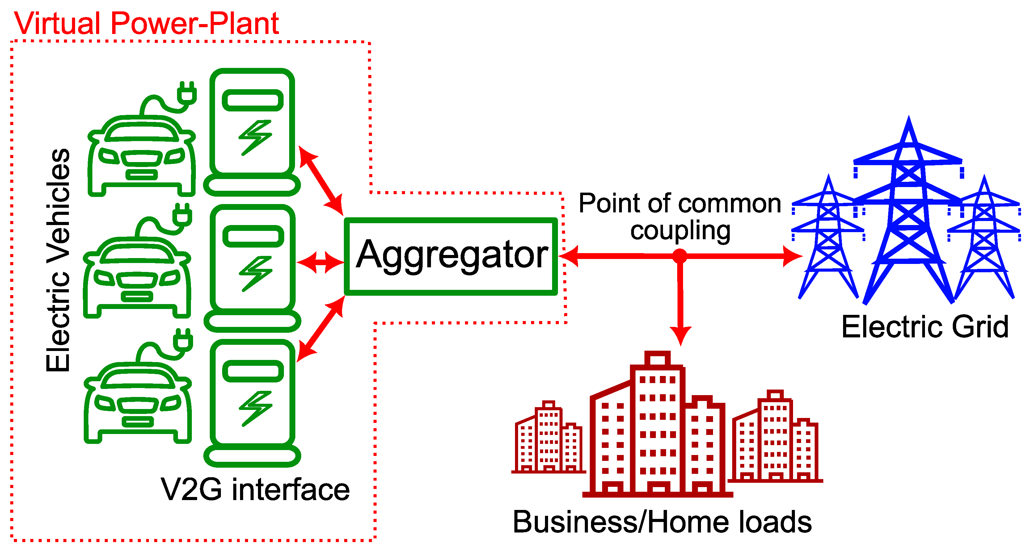
Figure 1 illustrates a VPP infrastructure using EVs in V2G mode. This allows EVs to bidirectionally transfer power to the grid or to loads via a V2G/G2V interface, serving as a distributed energy resource. The function of aggregators is to manage the operations between the grid and EVs, including regulations of the electricity market related to consumption and production [
9]. In this sense, efficient and flexible bidirectional V2G/G2V interfaces are essential for the implementation of VPPs, which require flexible and bidirectional power electronics interfaces.
In this context, multiple power converter topologies can be used to connect EV batteries to the grid [
10]. Among these, impedance source inverters (ISIs) stand out as single-stage converters and have been investigated in multiple recent works in the literature [
11]. ISIs present interesting features for EV charging stations, with flexible energy conversion, modular scalability, and better fault tolerance [
12]. Their operational mode extends the capacity of the inverter to synthesize AC voltage, allowing voltage buck and boosting to occur in one stage, tackling the limits of traditional inverters [
13]. Derived topologies such as Quasi-Z-Source and Y-Source networks further enhance energy transfer, allowing continuous input current and increased voltage boost, which are desirable characteristics for charging of EV batteries, reducing stress and extending system life [
14]. Moreover, the single-stage ISI design reduces the power conversion stages, which helps to improve reliability [
15]. In particular, Y-Source and Quasi-Y-Source inverters stand out in high-voltage gain and operational flexibility scenarios, due to the presence of coupled inductors [
16], which also help to obtain low shoot-through duty cycle ratios, minimizing switching losses and improving energy efficiency [
17].
Recent research has emphasized the role of ISIs in enabling the integration of EVs into VPPs through advanced converter topologies. Existing studies have demonstrated their advantages in improving reliability and performance in multisource EV systems [
18], as well as their ability to handle variable voltage inputs and support efficient battery interfacing in hybrid energy scenarios [
19]. Other contributions have proposed modulation techniques and alternative designs to improve efficiency, voltage gain, and system stability in EV applications [
20,
21]. Although these works confirm the versatility of ISIs, they mainly focus on specific converter variants or application-oriented improvements. In contrast, there is still a lack of detailed design methodologies and integrated control strategies tailored for Quasi-Y-Source inverters (QS-YSIs) in VPP-oriented EV applications, which is the gap addressed in this paper. This paper addresses this issue by demonstrating how to apply the QS-YSI topology designed for G2V and V2G operation in VPP contexts. Therefore, the main contributions of this work are as follows:
Proposition of a DC-link voltage controller and inverter output current controller in frame, taking into account the dynamic characteristics of the pulsating DC link voltage of the QS-YSI.
A seamless and decoupled integration methodology of DC-link and inverter output current controllers in G2V and V2G operations, considering the provision of reactive power compensation.
Design of a QS-YSI including the impedance source network components and inverter output LCL filter, considering a typical V2G/G2V application.
This paper is structured as follows.
Section 2 introduces the Quasi-Y-Source inverter (QS-YSI) system, detailing its converter topology, impedance network configuration, equivalent circuit models in different operating states and a comparative qualitative analysis with other conventional power electronics converter topologies used in such applications.
Section 3 presents the component design methodology, including analytical derivations for the Quasi-Y impedance network, design equations for the LCL filter, and practical design of components such as inductors and capacitors.
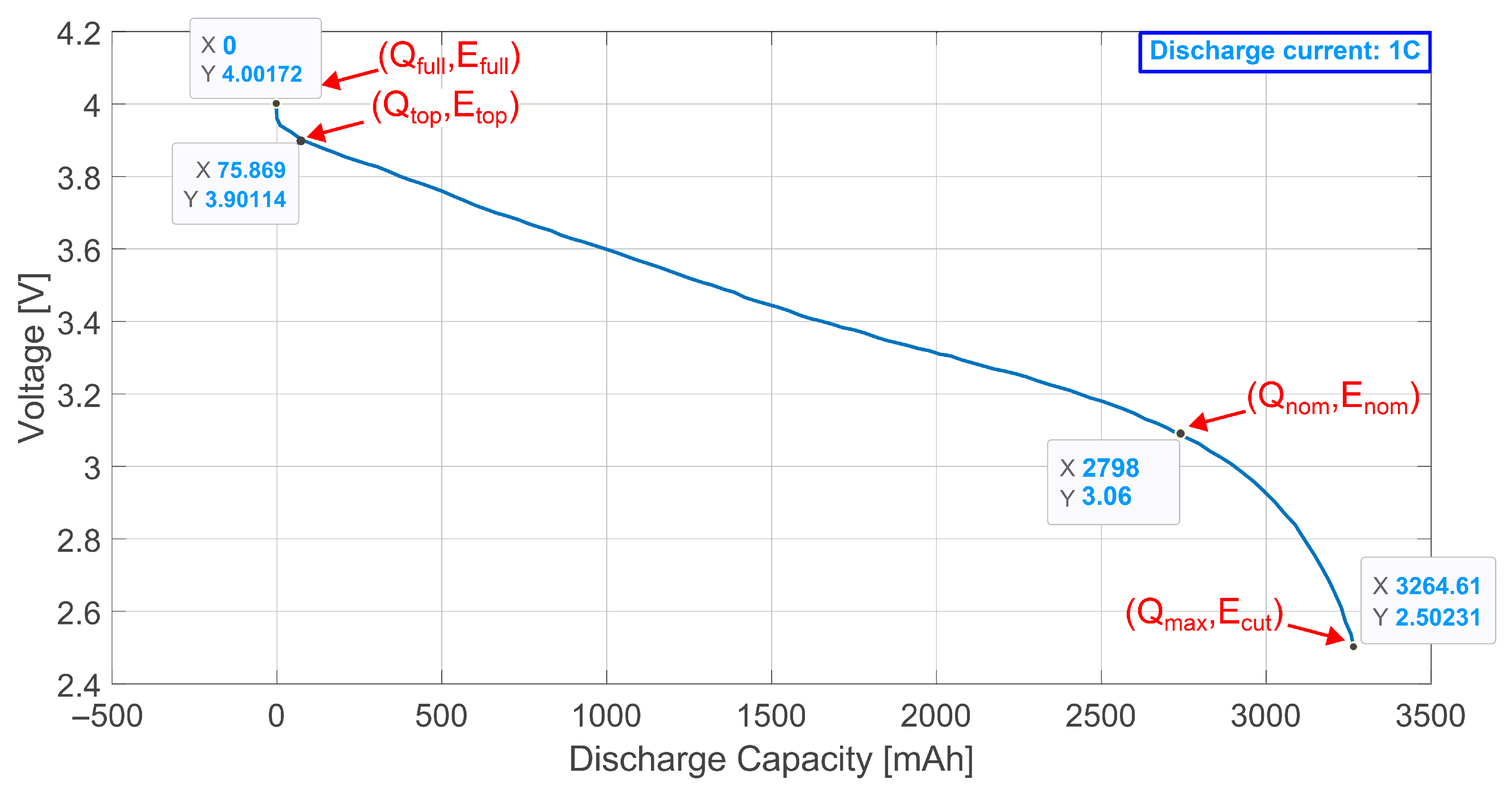
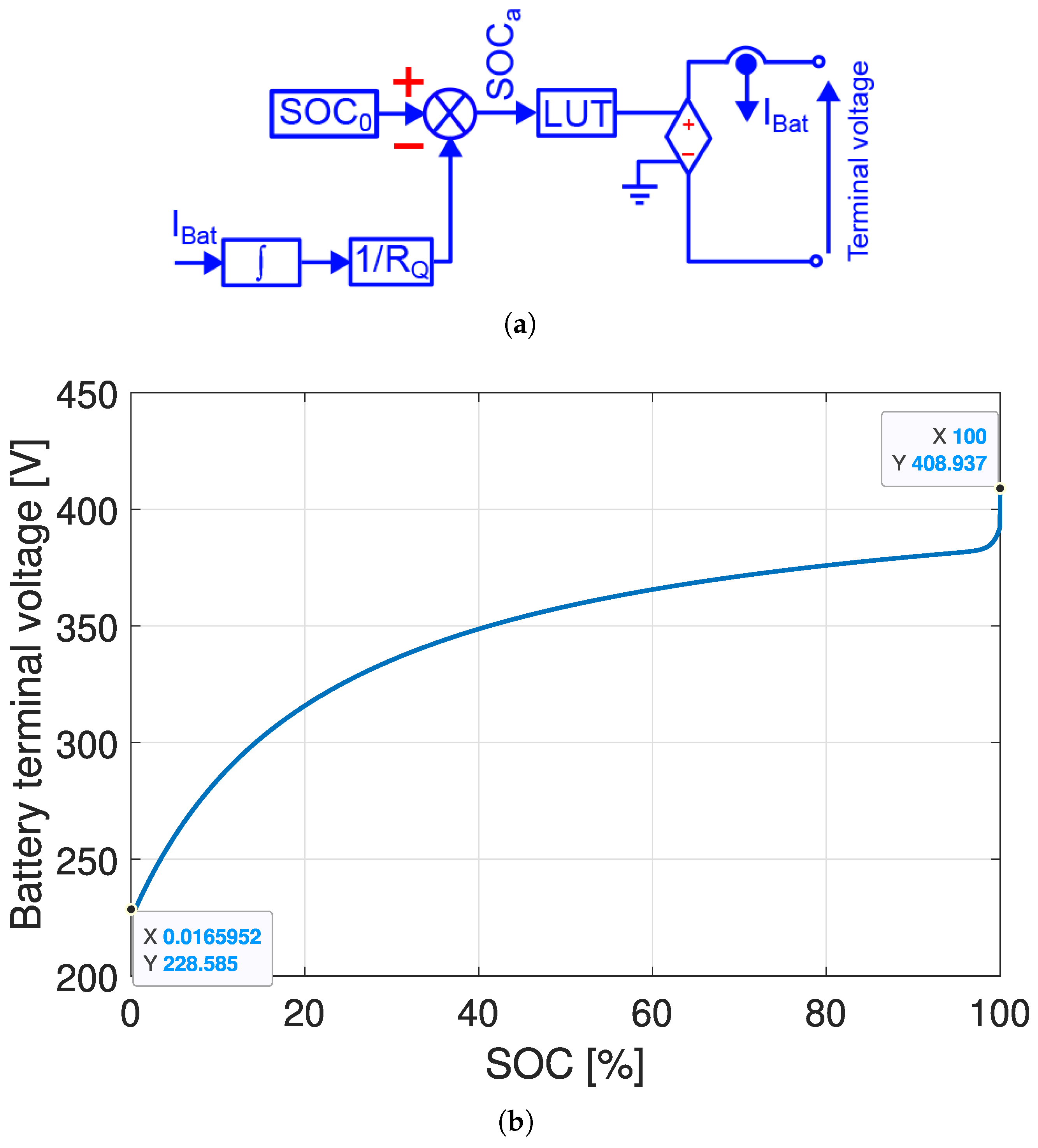
Section 4 describes the system parameters’ definition, covering the EV battery modeling, calculation of QS-YSI components including the LCL filter and the connected grid load that models business/home loads.
Section 5 discusses the proposed control strategy, covering the design of the DC-link voltage PI controller, the control of the inverter output current in the synchronous reference frame
, and the implementation of a modified PWM technique that decouples the control of the DC-link and the inverter output current.
Section 6 outlines the simulation setup and validates the system performance under two operational scenarios: bidirectional power exchange and reactive power compensation.
Section 7 presents experimental results using a small-scale prototype operational under nominal voltage conditions.
Section 8 provides a discussion of the obtained simulation and experimental results and design trade-offs, and
Section 9 concludes the paper, summarizing the main contributions and suggesting future research directions.
2. Converter Topology and Operating Principle
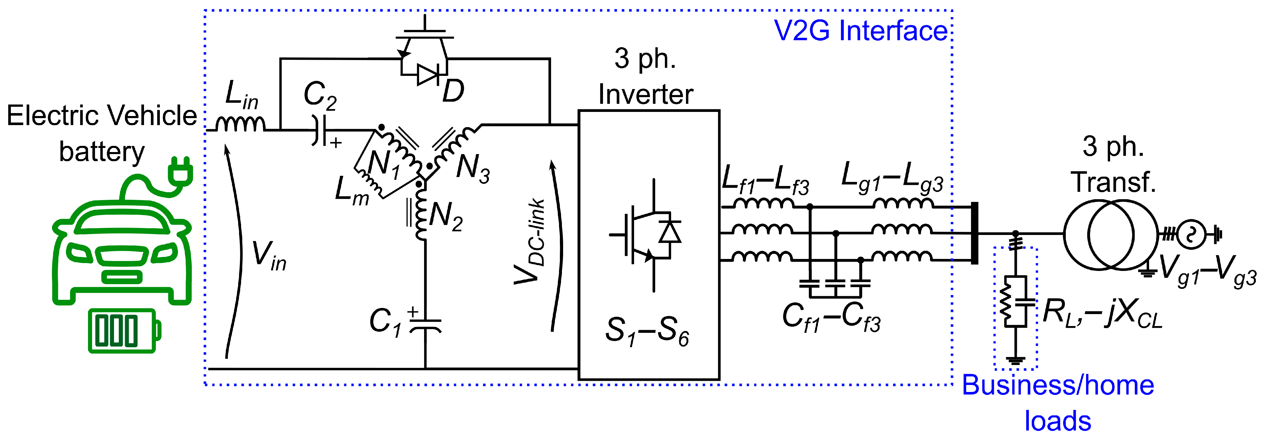
Figure 2 illustrates the bidirectional QS-YSI topology for EV V2G/G2V applications, configured for the connection of a three-phase grid using a galvanic isolation transformer connected to the grid, with phase voltages
–
. To model business and home loads, a three-phase load connected in wye and composed of a resistive impedance (
) and capacitive impedance (
) is connected at the point of the common coupling. The inverter stage employs a three-phase full bridge arrangement with six transistors
–
to generate the inverter output current output, filtered by an LCL network of inverter side inductors (
,
,
), intermediate capacitors (
,
,
), and grid-side inductors (
,
,
) to reduce high-frequency switching harmonics before grid connection. On the DC side of the inverter bridge, there is the impedance network, which is the key part of the energy conversion stage, whose components are described in the following. The input inductor
allows for continuous current at the input stage, and the diode
D prevents short circuits between the input stage and the inverter bridge transistors during the shoot-through operation mode. To allow bidirectional energy flow, there is an antiparallel transistor with diode
D, which is turned on when the EV battery needs to be charged (G2V mode). The impedance network also contains three coupled inductors with the turns ratio given by
:
:
and magnetizing inductance
, along with capacitors (
,
).
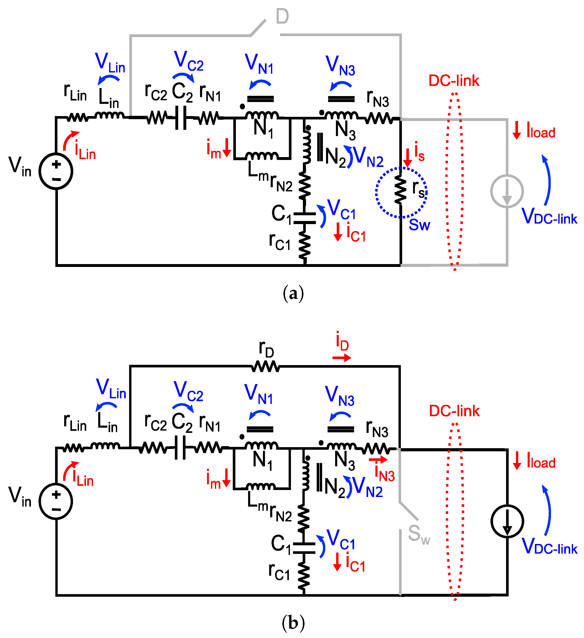
When operating in continuous conduction mode (CCM) with reduced leakage inductance values, the QS-YSI operating stages can be defined by shoot-through and active stages, whose equivalent circuits for both operating stages are presented in
Figure 3. The shoot-through stage is the one defined when the transistors of the same inverter bridge leg are turned on simultaneously, creating a short-circuit condition, whereas the active stage is the conventional inverter operation. Therefore, in
Figure 3, the switch
represents the shoot-through conduction mode of the three-phase inverter bridge. The load dynamics is modeled as a current source
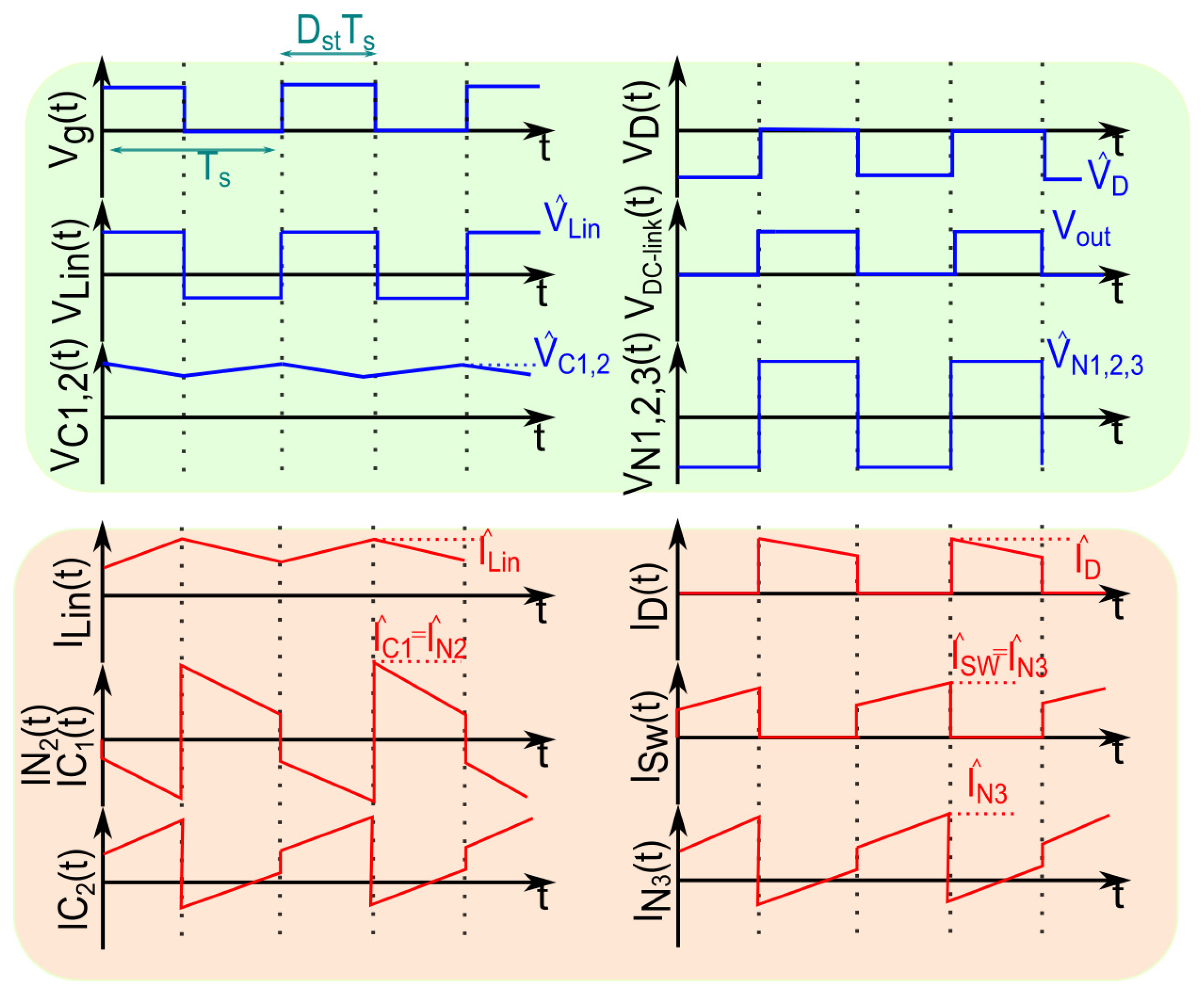
, and the corresponding voltage and current waveforms are illustrated in
Figure 4, where
denotes the shoot-through duty cycle,
the switching period, and
the gate signal for
, which remains high during the shoot-through interval and low during the active state. As can be seen in
Figure 3a, in the shoot-through state, with
conducting and diode
D blocked, the input energy is transferred to the coupled inductors, while the capacitor
discharges, rendering the load current independent of the input. Now, during the active state, as described in
Figure 3b when
D is turned on and
is turned off, the capacitor
is charged and the input voltage
energy is delivered to the load through
D, supplemented by the energy previously stored in the coupled inductors via the DC link. As indicated in the literature [
22], the ideal voltage gain of the QS-YSI converter is expressed as
, where the coupled-inductor factor is defined as
.
Comparison with Other Conventional Topologies for V2G/G2V Applications
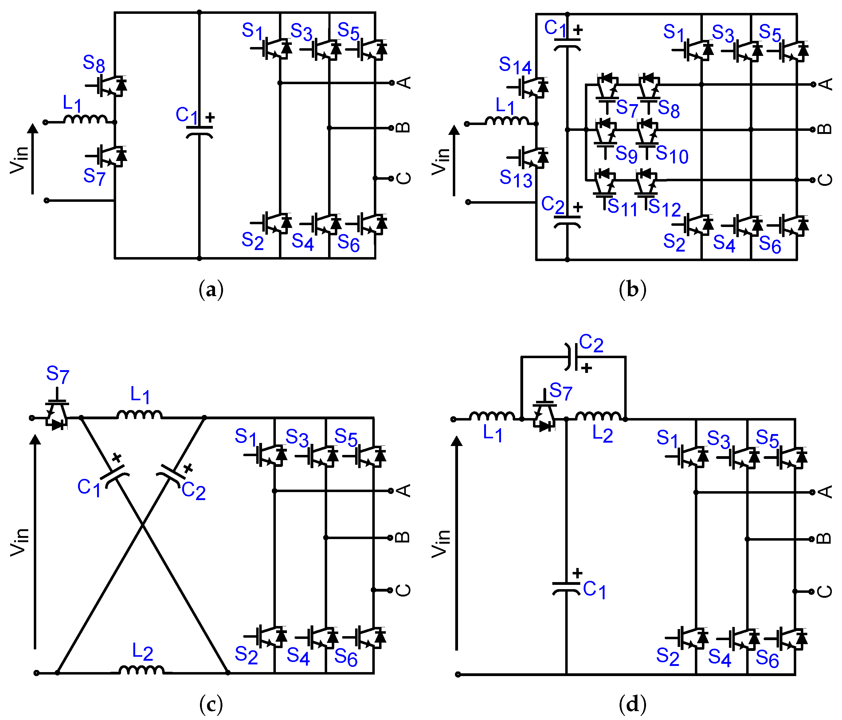
Figure 5 shows conventional bidirectional power electronics topologies used in EV applications, representing the two-stage full-bridge three-phase inverter, or Boost VSI (
Figure 5a); the T-type inverter (Boost T-type) (
Figure 5b); the Z-Source impedance inverter (
Figure 5c); and the Quasi-Z-Source inverter (
Figure 5d).
Table 1 shows a qualitative comparison among these topologies compared to the proposed QS-YSI presented in this work.
As indicated in
Table 1, conventional two-stage solutions such as a DC/DC boost stage followed by a VSI or T-type inverter require a dedicated boost converter to achieve voltage step-up, which depends on the duty cycle
adopted, which increases the complexity of the overall system. In contrast, impedance source families (Z-Source, Quasi-Z-Source, and Quasi-Y-Source) inherently provide buck-boost capability through their impedance networks, enabling single-stage power conversion.
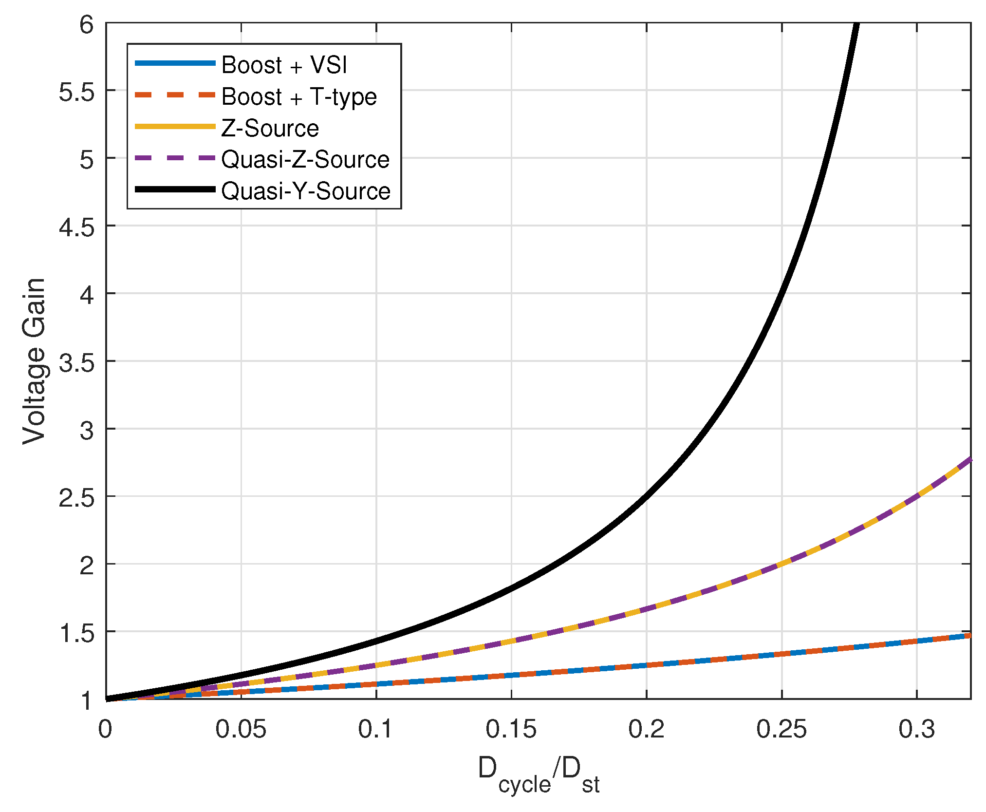
Moreover, the classical Z-Source inverter achieves voltage gain through shoot-through states but typically operates with a discontinuous input current (DCM), which increases the stress in the EV battery. Alternatively, the Quasi-Z-Source topology improves this by ensuring CCM, thus reducing stress and improving compatibility with EV batteries. However, both structures have limited boost capability at moderate shoot-through duty cycles
, when compared to QS-YSI, as can be seen in
Figure 6, which depicts the ideal voltage gain.
The proposed QS-YSI inherits the advantages of the Quasi-Z-Source—namely, CCM, shoot-through tolerance and single-stage conversion—while providing higher voltage gain due to the use of coupled inductors and its winding proportion ratio factor given by . This feature allows the same boost level to be achieved with a lower , which reduces switching stress and improves efficiency. Moreover, the QS-YSI has superior voltage gain characteristics and operational flexibility, making it especially attractive for EV V2G/G2V applications where high step-up capability and reliable bidirectional operation are required.
5. Proposed Control Strategy
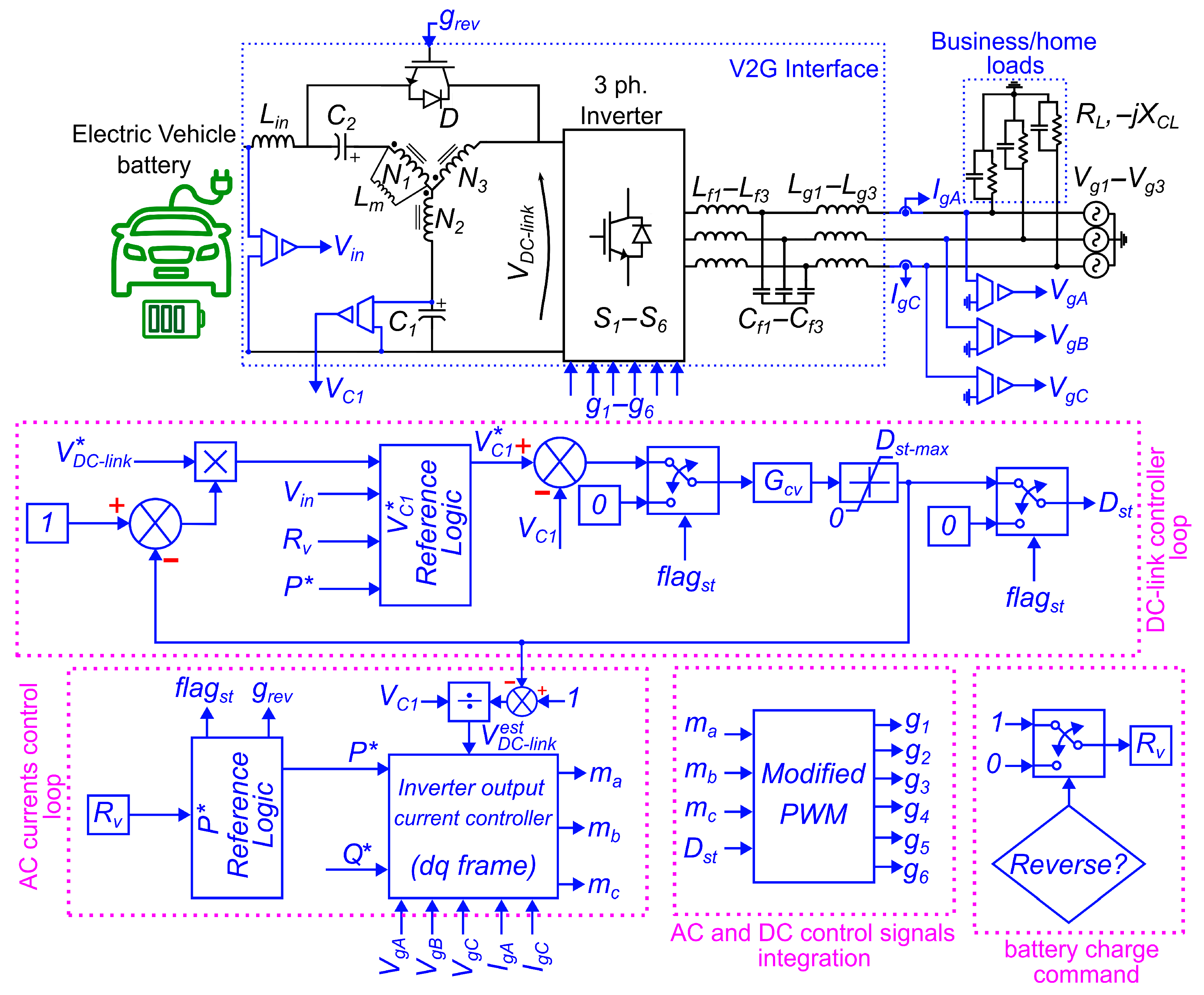
In this section, the proposed control strategy is presented, using a multi-loop architecture to regulate both the DC link voltage and the inverter output currents injected into the grid in a QS-YSI, as shown in
Figure 9. The controller
is designed for the DC-link voltage based on the frequency domain method, with control parameters tuned to ensure greater system stability margins due to the converter’s non-minimum phase behavior. On the AC side, the control operates in the synchronous
reference frame, enabling the decoupled regulation of active
and reactive
power references through independent PI controllers. The inverter output current controller relies on readings of the grid voltages
-
and the inverter injected currents
and
, where
is obtained mathematically. The reference currents for the
d and
q axes are calculated using the reference power commands
and
and the components of the voltage and current of the grid in the
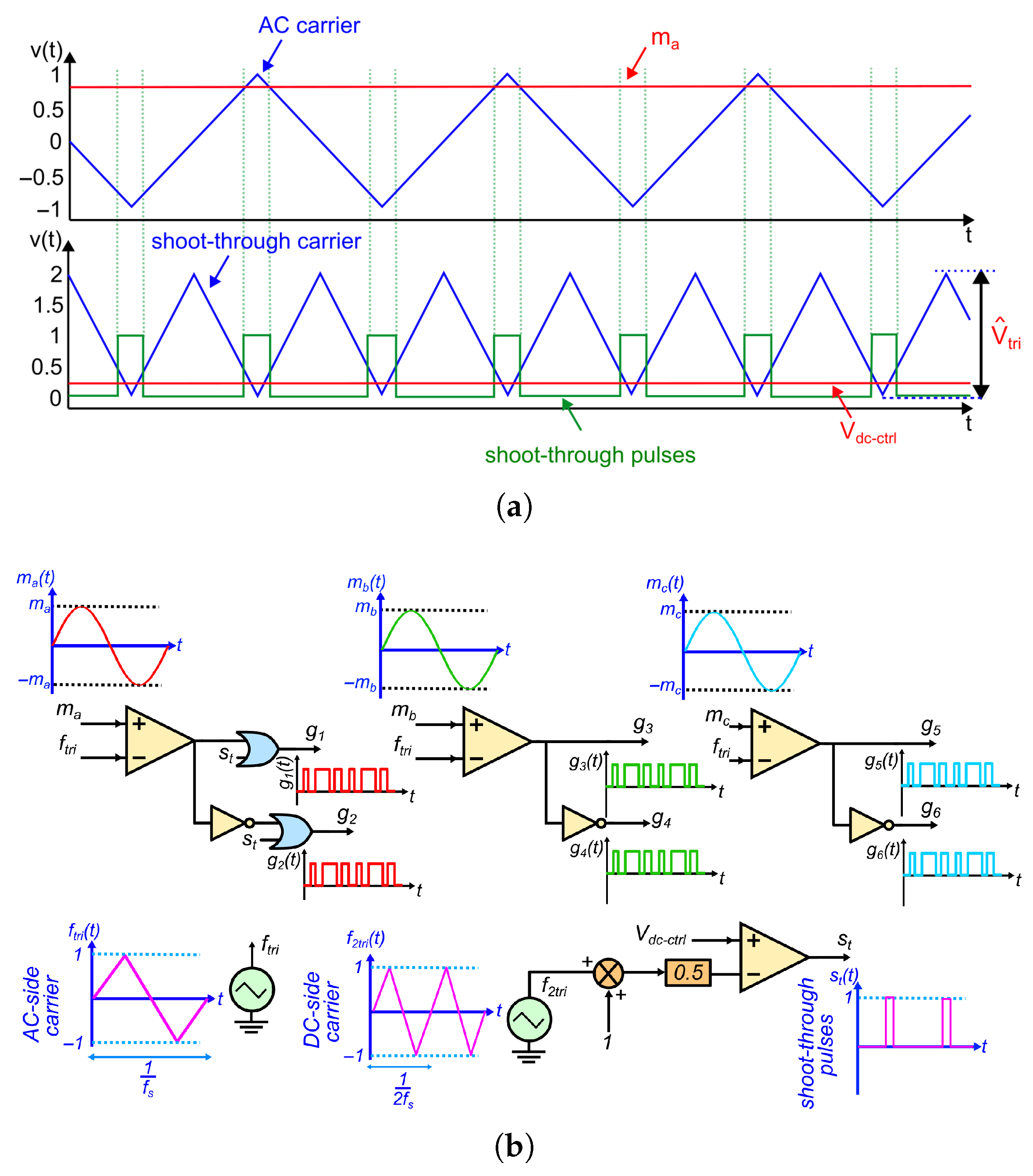
frame. To allow integration between the DC and AC control signals in the conventional SPWM technique, a modified PWM method is described that uses two distinct triangular carriers, one dedicated to the DC-link voltage control and another to inverter output current control, achieving a decoupled and simplified controller design. The complete system is synchronized with the grid through a phase-locked loop (PLL), which supports precise and stable bidirectional power exchange for V2G applications. In
Figure 9, the PLL and Park transforms are inside the inverter output current controller block.
As can be seen in the “
reference logic” and “
reference logic” in
Figure 9, the way that
and
behave changes if the active power flow changes from the battery to the grid (V2G) or from the grid to the battery (G2V). If the control system is required to operate in the V2G mode, then the voltage reference of the capacitor
is calculated in terms of the desired DC link voltage, according to (
14). In contrast, the DC link voltage is dynamically estimated in terms of the actual
voltage, according to (
15).
If the control system is required to work in G2V mode, then the flag is turned to 1; otherwise, it is 0. If is 1, then the DC link controller loop is’stopped’ by means of the control flag and the control signal for the anti-parallel transistor in the impedance network is turned to one, allowing the G2V operation. Furthermore, to avoid excessive current transients at due to stored energy in the impedance network components, gradually decreases to , and if the system was previously working in V2G mode, gradually decreases to a negative value, depending on the amount of power that should be injected into the battery. Finally, to avoid unwanted excessive values for , a saturation bounds the excursion of from 0 to . In the next sections, a detailed design methodology for the components of the proposed control system is given.
5.1. DC-Link Voltage Controller Design
Figure 10 shows the block diagram of the DC link voltage control of the QS-YSI. Taking into account the impedance network specifications outlined in
Table 6, the uncompensated open-loop transfer function, represented as
in the continuous domain, is defined by (
16), where the PWM dynamics
is modeled as a delay of one sample, with a transfer function given by (
17). The transfer function for the voltage
to the control signal
is specified by (
18), already considering the parameters of
Table 6. The
transfer function is derived from a state-space average small-signal model, which was derived by the authors in [
23].
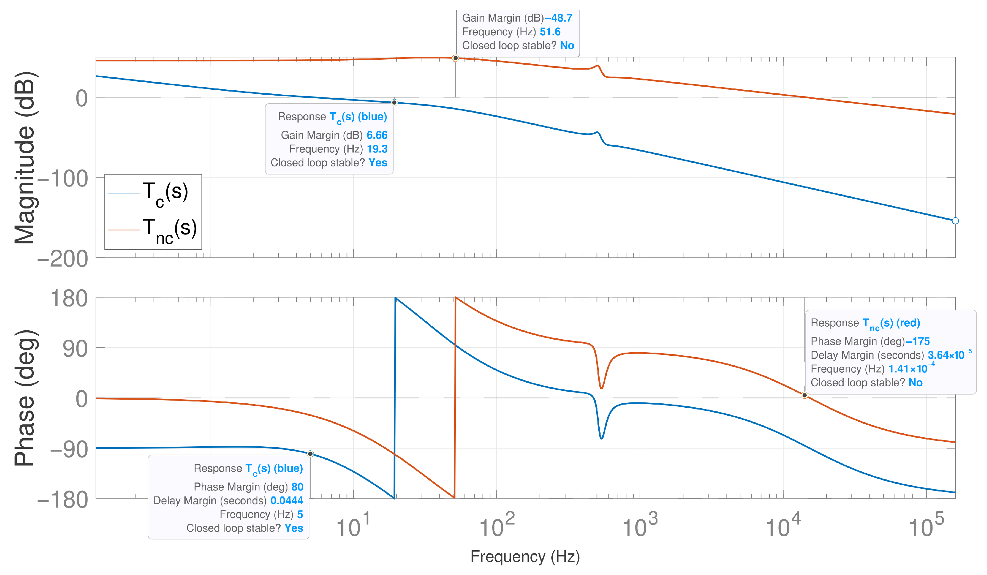
Figure 11 presents the Bode plots for the compensated open-loop function
and
. Before controller design (
), the Bode plot of
, shown in
Figure 11, reveals that it exhibits a negative gain margin (−48.7 dB) and a negative phase margin (−175°) at 14.1 kHz, indicating closed-loop instability and requiring proper controller design. Moreover, the existence of a non-minimum phase complicates controller design as it demands extensive phase inclusion at high frequencies to broaden the controller bandwidth. To modify these characteristics, a voltage controller
is designed to track the reference voltage. However, for non-minimum phase systems, such as the QS-YSI analyzed here, achieving a higher bandwidth frequency
without causing closed-loop instability is not always feasible. Therefore, a value of
= 5 Hz is chosen, which gives a satisfactory dynamic response and robustness to changes in operational conditions. A higher phase margin
results in a more damped response with an extended settling time, whereas lower values lead to a faster settling with potential overshoot and oscillations. Thus, a
of 80° is selected for this design, prioritizing damping over response speed. Following the method outlined in [
29], a type–II PI controller was designed for
in the continuous-time domain, considering the design requirements described before. The controller
transfer function is given in (
19). After the inclusion of
, as can be seen in
Figure 11, the compensated open-loop gain
presents a phase-margin of 80° at 5 Hz and a gain margin of 6.66 dB, achieving closed-loop stability and meeting the design requirements.
5.2. Inverter Output Current Control in dq Frame
The
or Park transformation expresses three-phase quantities, such as the injected currents of the grid
and the grid voltages
, in a rotating reference frame, simplifying the analysis in the phasor domain. This transformation is expressed by (
20), where
x can be a current or voltage variable. In the
domain, the complex power is defined as (
21), with ∗ denoting the complex conjugate and the vectors of complex voltage
and current
defined by (
22) and (
23), respectively.
Substituting (
22) and (
23) into (
21), the complex power of the grid
can be formulated as (
24). From (
24), the active
and reactive
powers can be isolated as (
25) and (
26), respectively.
Solving (
25) and (
26) for
and
, the direct and quadrature current references
and
can be calculated as (
27) and (
28), respectively. Therefore, given
,
,
, and
, it is possible to compute the reference values for
and
, respectively.
Taking into account that the impedance branch composed of
has a high impedance at the fundamental frequency,
control of the three-phase inverter with the LCL filter can be adapted from the conventional LC or L filter schemes, that is, it is assumed that the total inductance is the sum of the inverter and the grid inductance,
. In the same way, the equivalent total series resistance
. Therefore, inverter synthesized voltages can be written as (
29)–(
31).
Applying the Park transform in Equations (
29)–(
31), one can obtain (
32) and (
33), which describe the synthesized inverter voltage in the
reference frame. Taking the Laplace transform of (
32) and (
33), one can obtain (
34) and (
35), which describe the dynamics of
and
, respectively, in the complex frequency domain. However, it can be seen from (
34) and (
35) that by adding the feed-forward gains
and
to (
34) and
and
to (
35), the system is decoupled, and the variables
and
are only controlled by
and
, respectively, as shown by the block diagram in
Figure 12 (which is the same for the design of the PI controller for
and
). Since the system shown in
Figure 12 is a type 0 system and
and
are usually given as constant values, a null steady-state error in a closed-loop system can be achieved with a simple PI controller.
Therefore, the following design requirements are defined to obtain the PI controllers for the inverter current control loop in the
frame: a bandwidth frequency
= 240 Hz which is set three decades below
and a phase margin
set at 60°. The designed
transfer function is given by (
36) and was obtained using traditional design rules for the frequency domain response [
30].
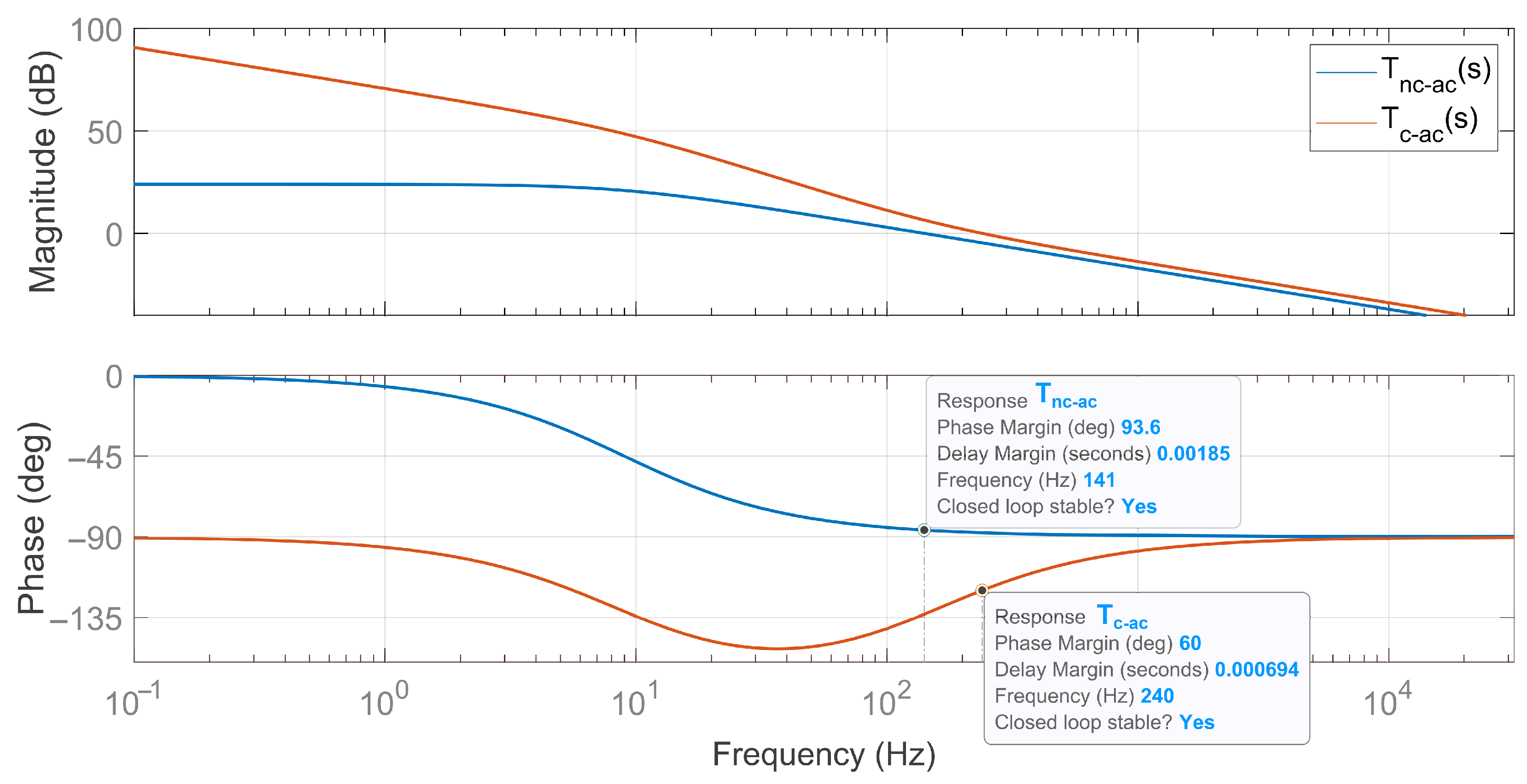
Figure 13 shows the Bode plots of the uncompensated open-loop gain
and the compensated open-loop gain
, considering the block diagram shown in
Figure 12. It can be seen in
Figure 13 that both
and
have infinite gain margins and are closed-loop stable, but the uncompensated loop
has a value of
of 93.6°, while
has 60° of
at 240 Hz, thus indicating the successful design of
.
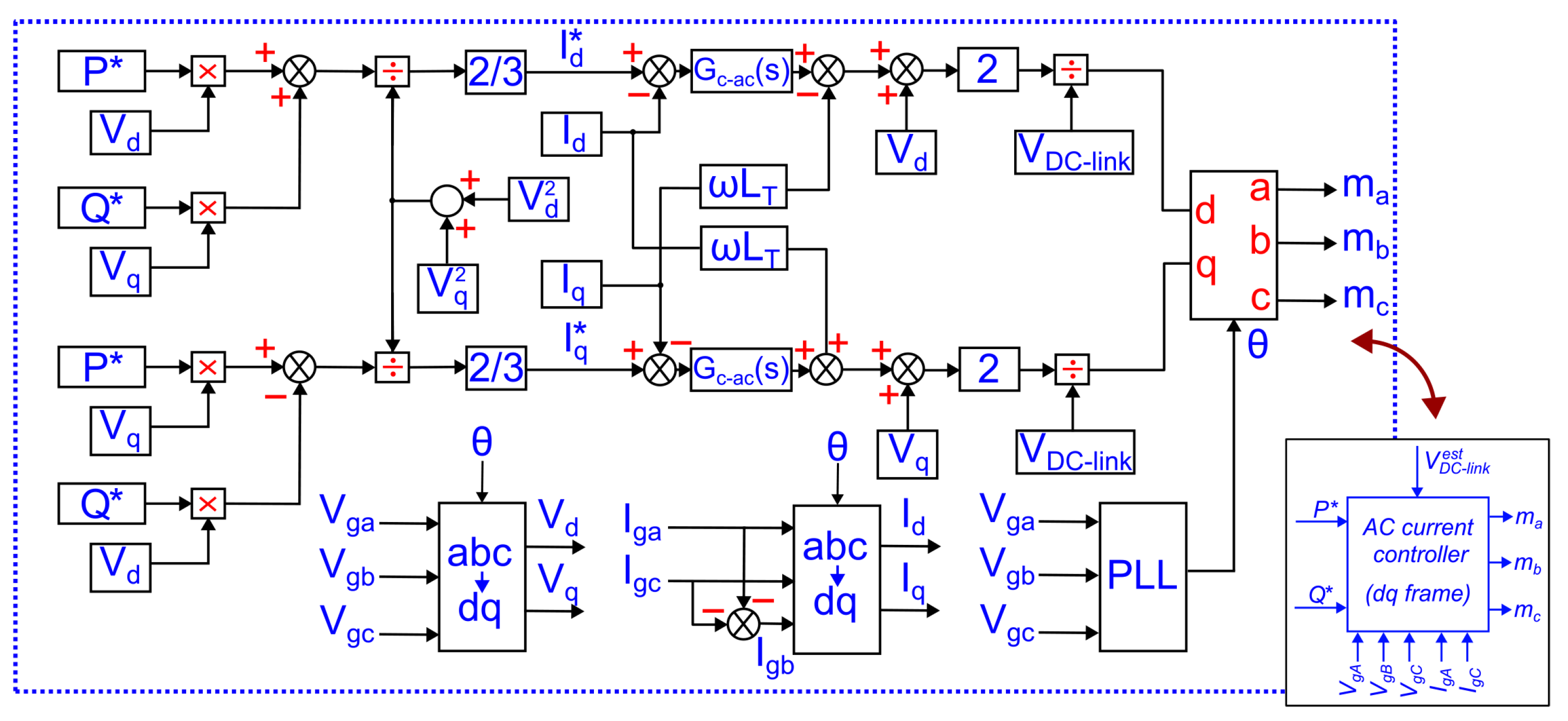
The control architecture shown in
Figure 14 shows the complete block diagram of the inverter output current controller in the
frame, indicating the content of the block “inverter output current controller” shown in
Figure 9. The PLL processes the three-phase voltage inputs
,
, and
to estimate the instantaneous grid angle
, which is then used to transform the measured grid voltages into the frame components
,
, and
. The same is true for the grid currents
and
, where
is obtained mathematically from
and
. The control objective is defined by the active and reactive power references
and
. These references are used in combination with the measured voltage components to compute the reference currents
and
, using (
27) and (
28). The
controllers designed before regulate the output currents of the converter by minimizing the error between the reference currents
and
and the actual currents
and
, respectively. The controller outputs are subsequently transformed back into the three-phase
frame through inverse Park and Clarke transformations, using the angle
provided by the PLL. The resulting modulation signals
,
, and
are used to generate SPWM gating signals
–
.
5.3. Modified PWM for Shoot-Through Integration
Table 7 presents expressions for determining
for various carrier-based modified SPWM techniques commonly found in the literature for ISIs [
31]. For these techniques, the control variable
not only establishes the control of the DC bus by determining the shoot-through duty cycle but also limits the linear modulation index
M used to synthesize the sinusoidal modulating wave and consequently control the magnitude of the fundamental component of the voltage generated by the QS-YSI, as will be discussed later. As can be seen from the expressions presented in
Table 7, the transfer function
cannot be obtained directly, which indicates that there is no decoupling between the control information related to the DC-side and the AC-side control of the converter, thus complicating the controller design.
In this sense, ref. [
32] proposes a modified SPWM technique that allows a direct expression of
and provides decoupling between the control of the DC side and the AC side of the inverter.
Figure 15a presents the waveforms for the modified SPWM strategy proposed by [
32], and
Figure 15b presents the block diagram that implements this strategy. It can be seen that two distinct triangular carriers are now used, unlike the SBC, MBC, and MCBC techniques, which use only one. In this case, there is a triangular carrier
for the AC-side control, which interacts only with the linear modulation index
M and
for the DC-side control, which interacts only with the control signal for the regulation of the DC bus,
. In this way, there is decoupling between the control signals of the DC-link loop (
) and the AC sides (signals
,
and
), which allows for a direct relationship between
and
given by (
37), which facilitates the design of the controller for the regulation of the DC bus. The triangular carrier
has twice the carrier frequency on the AC side to ensure that shoot-through conduction will occur only for zero-voltage switching configurations of the inverter. Furthermore, keeping the magnitude of this carrier
equal to 2, the controller output command
becomes numerically equal to
, as can be observed from (
37). The proposed modified SPWM scheme is developed based on the simple boost control strategy, and the maximum values of the control variables
and the maximum allowed shoot-through duty cycle
are related by Equation (
38).
7. Experimental Results
In this section, preliminary experimental results are shown for the proposed system, considering a small-scale prototype operating with nominal voltage levels, with programmable sources acting as the grid and storage systems, respectively.
Table 8 shows the prototype parameters, which are different from
Table 6 due to the power scale capability of the prototype and the limitations of the components. The parameters shown in
Table 8 were used in the computer simulation using PSIM, with F28379D blocks for the configuration of ADC and PWM peripherals and the SimCoder package for automatic code generation. The PSIM code generator tool was used to create the controller C code, while Code Composer Studio was used to upload the code to DSC F28379D. The coupled inductors were built on a sendust toroidal core (
= 60 H/m) with a winding turn ratio of 37:112:186 and 2 × 22 AWG and 3 × 20 AWG Litz wires. The capacitors
and
were implemented with the A511EJ68M450F and the C4AQLLU5150A19K model of 15 μF, 500 V film capacitor. The IRG4PF50WD IGBT and GC2X5MPS12 26 A and 1200 V SiC Schottky diode were used as
and
D. During grid-connected tests, the inverter output passive filter comprised three inductors with 10 mH, being a first-order low-pass filter.
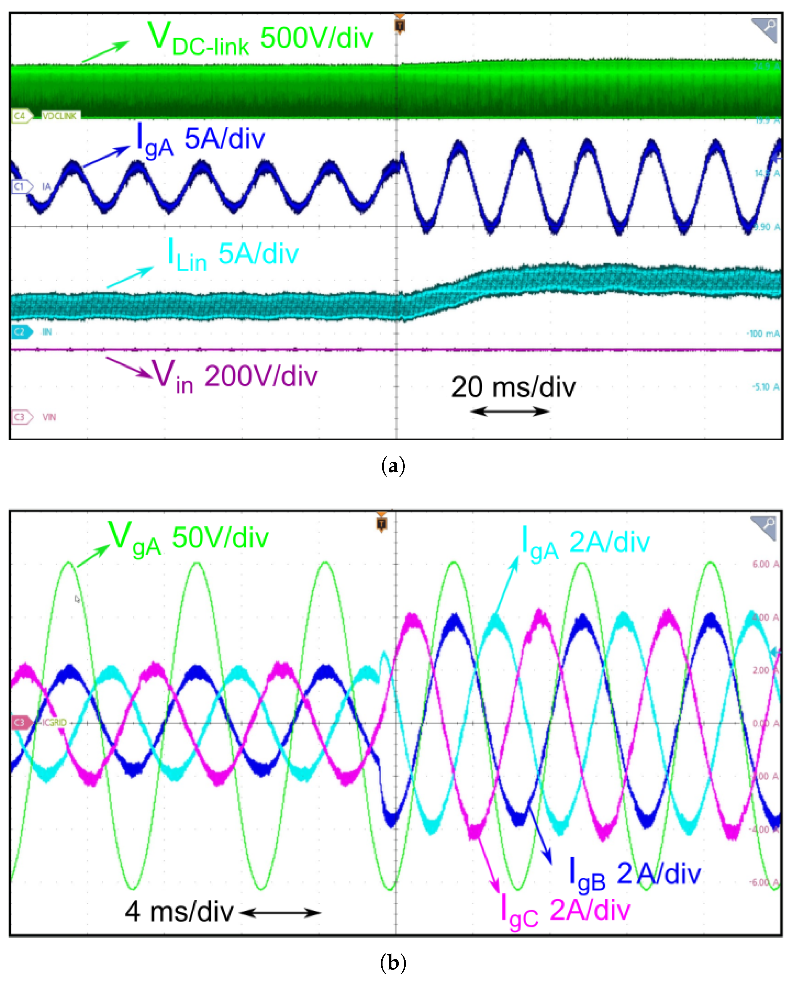
Figure 20a shows the waveforms obtained for
,
,
, and
, while
Figure 20b shows the inverter-injected currents and phase voltage for V2G operation and a step reference change in the injected current.
8. Discussion
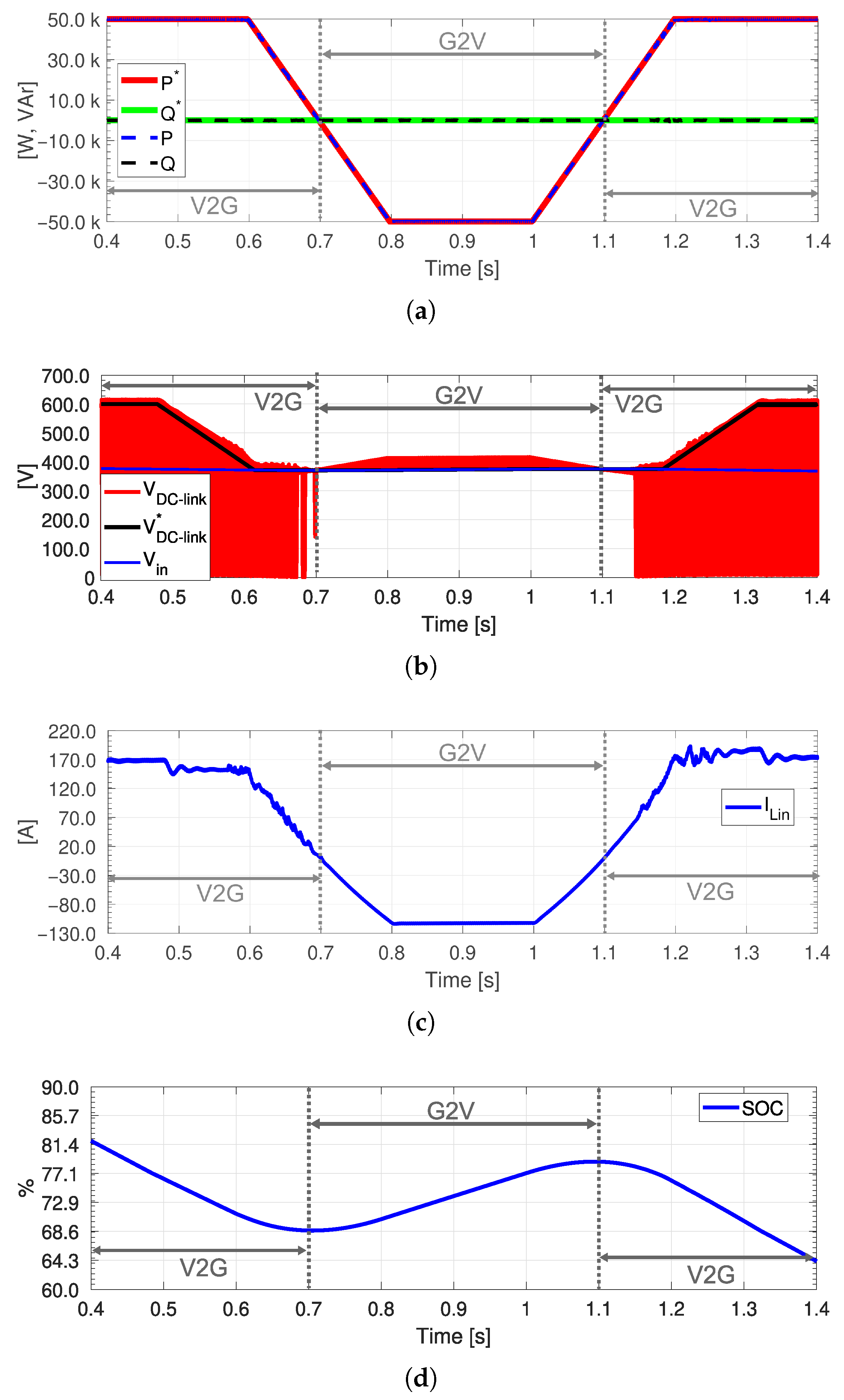
The results obtained for Scenario 1, shown in
Figure 16 and
Figure 17, clearly illustrate the effectiveness of the V2G and G2V operations of the proposed system. In Scenario 1, the QS-YSI successfully followed the active power reference
and
, resulting in only active power injection without reactive power exchange. Moreover, during power injection and charging, the EV managed 50 kW of active power transfer. The transition from V2G to G2V is smooth, using a reduction in the ramp for the power reference between 0.6 and 0.8 s and a ramp increase from 1.00 to 1.20 s, as shown in
Figure 16a. Furthermore, the
reference signal decreases in a ramp from 0.5 to 0.6 s and increases from 1.2 s to 1.3 s. This approach prevents excessive
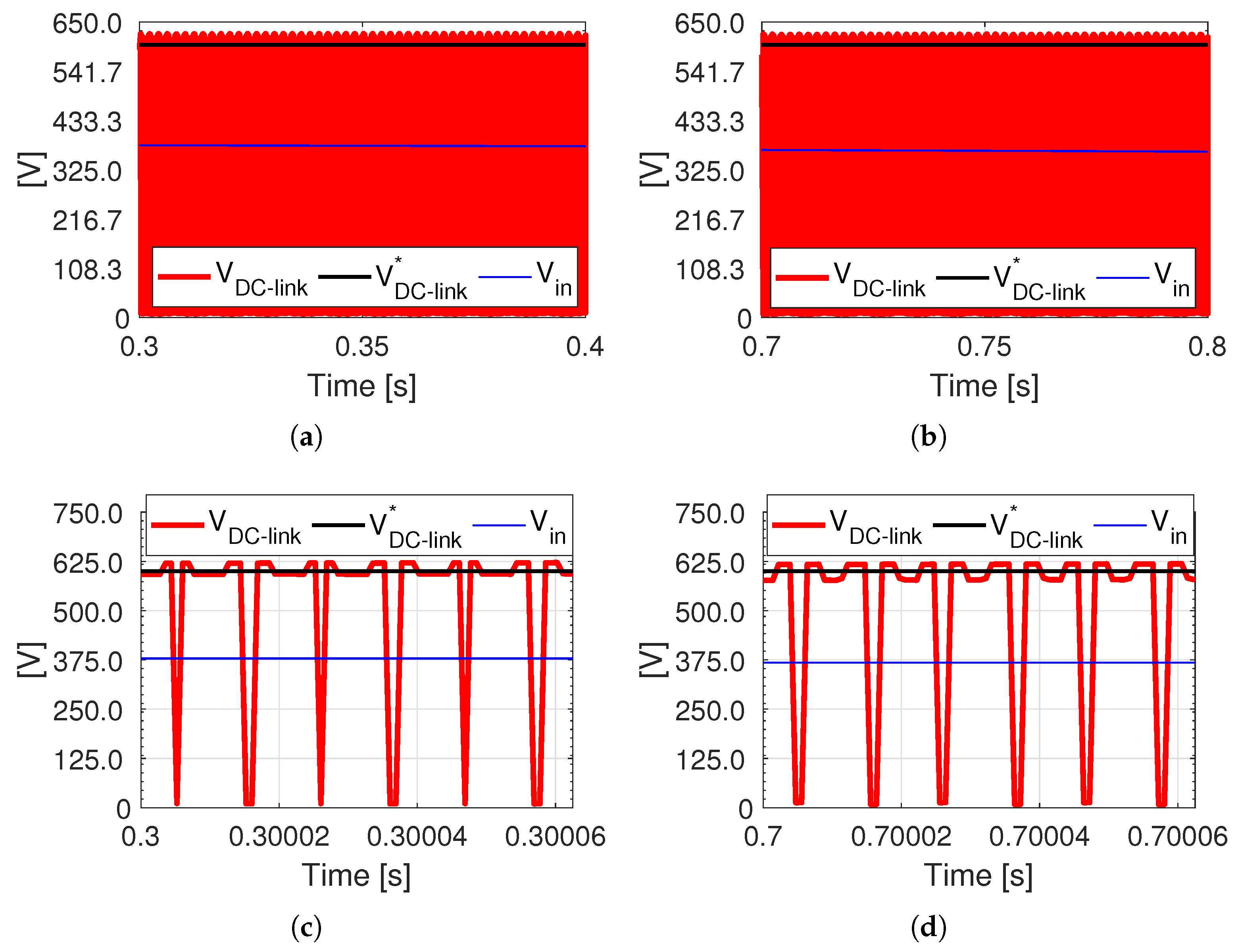
current spikes during the V2G to G2V transitions, by ensuring that any energy stored in the impedance network during V2G is removed before entering G2V. The reason for this is that during V2G, the QS-YSI operates in boost mode, amplifying the DC link voltage to approximately 600 V using the shoot-through state, as shown in
Figure 16b. However, the V2G to G2V transition involves a gradual adjustment of
to
, which reduces the values of
, thus decreasing the stored energy. This, along with active power reference ramping, ensures a seamless mode transition, which diminishes the spikes at
during the transients.
Figure 16c shows the waveforms
, highlighting nearly continuous operation with reduced ripple and oscillations during the change of the V2G-G2V modes. As can be seen, the input inductor
allows a continuous current flow, demonstrating the inherent benefit of QS-YSI to this type of application, which involves battery charging.
Concerning the battery dynamics,
Figure 16d illustrates the evolution of the state of charge (SOC) during transitions between the operational modes of V2G and G2V. As the system shifts from the V2G to the G2V mode, the SOC variation rate over time decreases progressively, highlighting a gradual reduction in the injection of energy into the grid by the EV, since the power reference is decreased, as discussed before. Between 0.70 s and 1.10 s, which corresponds to the G2V mode, the battery SOC increases from approximately 69% to 79%, indicating that the EV battery is being charged. After 1.10 s, the V2G mode is again enabled and the SOC decreases, since the battery energy is sent to the grid. This aspect confirms that the system operates as intended with regard to the transitions of both modes. As can be seen in
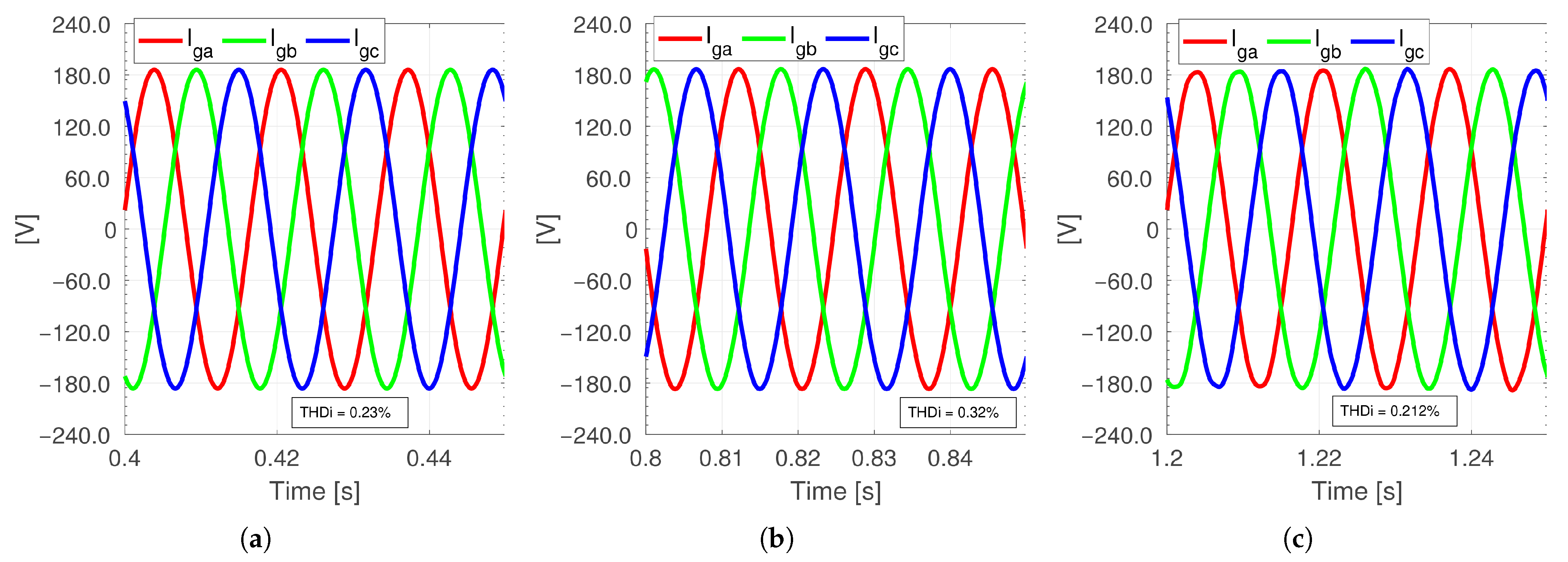
Figure 17a,c
remains between 0.21% and 0.23% in the V2G mode, while it reaches 0.32% during the G2V mode, as can be seen from
Figure 17b. This indicates that the implemented QS-YSI system successfully maintains a
profile under 5%, adhering to the harmonic standards [
33].
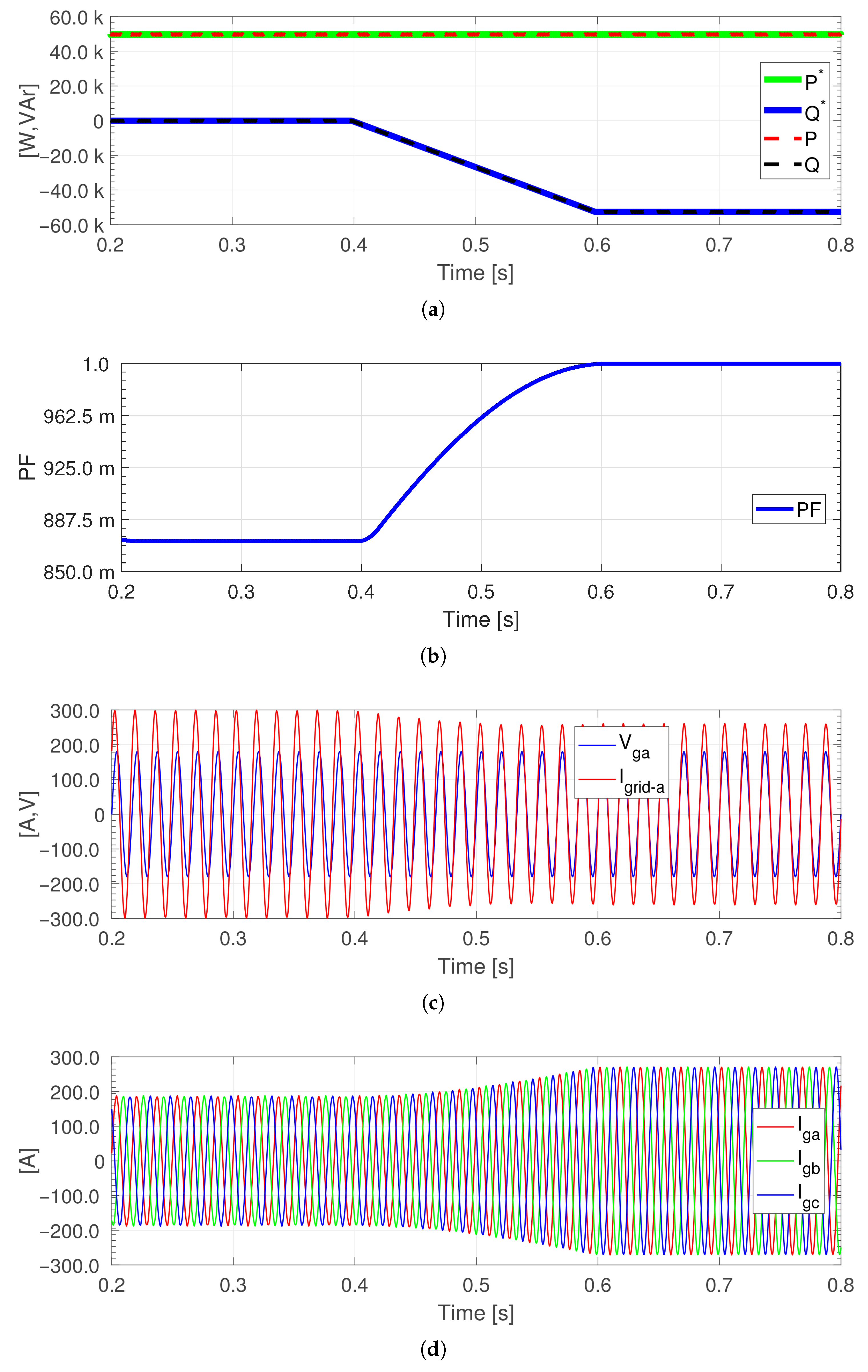
For scenario 2,
Figure 18a demonstrates the effective achievement of the reference signals of EV
and
. Initially, before 0.4 s, the EV injected only active power into the grid. Between 0.4 s and 0.6 s, the reactive power reference
gradually decreased, stabilizing after 0.6 s alongside
. This indicates efficient active power injection and ancillary service, improving the grid power factor from approximately 0.875 to 1, as shown in
Figure 18b. As can be seen in
Figure 18c,d, the grid currents decrease as the injected current of the inverter increases, and it can be seen from
Figure 18c that the phase current gradually becomes in phase with the phase voltage.
Figure 19a,b confirm that
accurately followed reference
; detailed waveforms of
before and after reactive power exchange are shown in
Figure 19c,d, revealing the effects of the active and shoot-through states.
From the experimental results,
Figure 20a shows the capability of QS-YSI to inject power into the grid, and it can be seen that the voltage
remains regulated at 470 V, reaching a peak value of 560 V after the reference change in
from 2 A to 4 A RMS. It is also possible to observe the reference tracking capability due to the inverter output current controller in
Figure 20b. Furthermore, the QS-YSI input current
remains in CCM mode throughout all operations, with a mean value that varies from approximately 2.5 to 4.5 A, while the input voltage
remains at 250 V. Regarding the inverter currents injected into the grid,
Figure 20b show the three inverter output currents,
–
waveforms, including the grid voltage
. It is clear from the comparison of the angular displacement of
with
that the inverter currents are injected with a power factor (PF) close to unity, which is mandatory for a grid-connected inverter. This was confirmed by the measured PF value of 0.997, obtained after the current reference change.
9. Conclusions
This paper introduced a Quasi-Y impedance source inverter (QS-YSI) specifically designed to operate as a Vehicle-to-Grid (V2G) and Grid-to-Vehicle (G2V) power electronics interface for EVs in the context of a virtual power plant (VPP). Based on the studies conducted, the main conclusions are as follows.
The proposed QS-YSI facilitates both V2G and G2V operational modes, enabling bidirectional energy transfer between EVs and the grid. This allows EVs to either supply power back to the grid or draw energy for charging, while also providing reactive power support.
Simulation scenarios and experimental validation demonstrate the capability of the inverter to exchange power with the grid and assist in the regulation of the power factor.
A detailed design methodology was presented for the impedance network elements, including operational principles and control system development. This considers pulsating DC link voltage regulation and inverter output current control in the frame, both integrated into a modified PWM scheme for decoupled operation.
The main contribution of this research lies in demonstrating how to design and control QS-YSI in V2G/G2V applications with reactive power compensation, leveraging its single-stage buck–boost capability, bidirectional operation, and continuous input conduction, all of which are advantageous for EV batteries.
However, this study did not address challenges commonly encountered with the implementation of impedance source inverters, such as leakage inductance effects, DC-link voltage spikes, the need for auxiliary snubber circuits, complexities in coupled inductor design, and EMI considerations. Although these issues can be mitigated with appropriate methodologies, a detailed treatment is beyond the scope of this work. Future research will address systematic benchmarking against alternative converter topologies, refined grid modeling, and extended experimental validation.
