Abstract
Power electronics has significantly contributed to advances in developing single-stage integrated converter topologies, enabling DC/AC conversion with voltage step-up capability in a compact and efficient structure. This work proposes a novel Integrated Zeta–Ćuk Inverter (IZCI), derived from combining the Zeta and Ćuk DC/DC converter structures. In addition, the proposed topology achieves high efficiency and full utilization of the input voltage. A potential application for the IZCI topology involves DC microgrids, in which the proposed topology can supply AC local loads, achieving high power quality, such as a low total harmonic distortion (THD). The IZCI operates in discontinuous conduction mode (DCM), exhibiting three distinct operating stages for each switching period. The DCM operation guarantees a linear relationship between output and duty cycle, simplifying the control strategy and requiring fewer sensors, thereby reducing the cost and processing requirements. The feasibility and performance of the IZCI topology are evaluated and validated through experimental results in a standalone application. The results demonstrate high energy conversion efficiency and reliability, providing an AC output voltage with low harmonic distortion.
1. Introduction
Experts consider renewable energy sources inexhaustible because they continuously regenerate during use. The most prominent sources are hydro, solar, wind, biomass, geothermal, and ocean energy [1]. In addition to being naturally replenished resources, renewable sources are also recognized for their low greenhouse gas (GHG) emissions, which characterize them as clean energy alternatives [2].
In light of the growing global effort to mitigate environmental impacts and promote a more sustainable energy matrix, renewable energy sources (RES) have gained increasing prominence, especially in conjunction with distributed generation (DG). Brazil stands out for its predominant use of RES, with particular emphasis on photovoltaic (PV) solar energy, which has been growing significantly in this scenario in recent years, resulting in lower GHG emissions and aligning with global efforts to reduce the environmental impact of fossil fuel-based power generation [3,4,5].
Current forms of energy generation require appropriate processing of the generated electrical power to enable its integration into various applications, such as battery energy storage systems (BESS) and distribution networks [4,5,6,7,8,9]. Power converters primarily perform this processing and act as the interface between direct current (DC) sources and alternating current (AC) loads [10,11].
In this context, recent advances in technologies applied to power electronics have significantly contributed to developing new static converter topologies, characterized by higher efficiency, flexibility, and performance, thereby expanding their potential for application in various technological scenarios [4,5,6,7,8,9,10,11,12].
In the current energy transition context, it is also essential to highlight microgrids, systems composed of distributed generation (DG) sources, local loads, and BESS [13,14,15]. These systems can operate autonomously or be connected to the primary AC power grid, enhancing the flexibility and reliability of the electrical system. Over the years, numerous proposals have emerged to advance microgrid development, leading to changes in their topological structures, control strategies, and functionalities to meet the requirements of diverse applications, such as aeronautical, maritime, rural, residential, commercial, and industrial environments [16,17].
DC-based microgrids have garnered increased attention due to their technical and operational advantages as part of this evolution. Their main benefits are elevated energy efficiency, simplified interfacing with RES and BESS, and high compatibility with modern electronic loads. The growing integration of RES and DG has contributed to the increasing complexity of modern electrical systems, demanding more dynamic, intelligent, and resilient solutions.
Accordingly, power converter structures have been extensively investigated and developed for various applications, driven by the growing use of RES, the increasing electricity demand, and the expansion of DC microgrids [18,19]. These studies aim to enhance the efficiency and stability of such systems in the face of the inherent challenges associated with integrating multiple energy sources and diverse loads.
Double-stage conversion systems are commonly employed to interface DC sources with AC systems. This configuration typically consists of a cascaded association of a boost converter followed by a voltage source inverter (VSI), enabling appropriate energy conditioning for delivery to the grid or end-use load [20,21].
Although this is a well-established and relatively simple solution, such architecture presents significant limitations, including the requirement of an intermediate DC bus with high capacitance, used to decouple both conversion stages. These factors increase physical volume and costs. They also hinder achieving high overall efficiency once the DC/DC and DC/AC conversion processes inherently involve conduction and switching losses, which become more pronounced due to the larger number of components and conversion stages [22,23].
As an alternative to the previously discussed limitations, several recent studies have investigated the development of integrated inverters capable of simultaneously performing input voltage boosting and DC/AC conversion [24,25,26,27,28,29,30,31,32,33,34,35,36]. These topologies are designed to meet increasingly stringent requirements in modern applications, such as operating with reduced volume and weight to facilitate integration into compact systems; achieving high DC/AC conversion efficiency to enhance energy utilization; and, whenever possible, minimizing the number of electronic components, thereby reducing cost, control complexity, and improving system reliability.
Among the integrated inverter topologies, the Single-Stage Common Ground Boost Inverter (S2CGBI) eliminates leakage current by employing a common ground between input and output [24]. Other structures, such as those proposed in [25], introduce direct coupling between the boost converter and a full-bridge inverter, thereby eliminating the need for large decoupling capacitances. Similar topologies, like the Buck–Boost Inverter (BBI) presented in [26], integrate DC/DC and DC/AC conversion functions using fewer components, contributing to a more straightforward and compact implementation.
Other approaches integrate classical DC/DC converters into single-phase inverter architectures. Ref. [27] proposes a structure based on SEPIC and Ćuk converters that enables alternating operating modes according to the output voltage half-cycle. Similarly, Ref. [28] presents an architecture derived from the Buck–Boost converter, which uses a single inductor for both half-cycles and operates in discontinuous conduction mode (DCM), resulting in simplified control and a reduced number of passive components. These approaches demonstrate the potential of creating novel topologies of integrated inverters based on traditional DC/DC topologies within integrated inverter configurations.
Among recent advances, notable contributions include the works of [11,29], which propose integrated inverters based on Zeta and Ćuk topologies, such as the Single-Phase Integrated Zeta Inverter (SP-IZI) and the Hybrid Zeta–Ćuk Inverter (HZCI). These topologies operate DCM and provide a regulated output voltage with low harmonic distortion. The coupling capacitors, combined with the alternating operation between Zeta and Ćuk modes, reduce current stress on the components and enhance conversion efficiency.
Hence, a similar topology composed of two modified Ćuk converters connected in parallel, enabling voltage step-up and unidirectional operation, was proposed in [30]. The modulation strategy adopted relies on sinusoidal pulse-width modulation (SPWM). In [31], the Integrated Ćuk Inverter (ICI) is presented as a DC/AC topology using hysteresis control and maximum power point tracking (MPPT) employing the perturb and observe (P&O) method. The converter operates in two half-cycles with three distinct switching stages, where the sequential control of the switches ensures efficient magnetization and demagnetization of the inductors.
Other studies, such as [32,33], strengthen the trend toward structural simplification and minimizing the number of passive components. In [32], an approach was proposed to eliminate electrolytic capacitors and introduce a common ground, thereby minimizing parasitic capacitance. Meanwhile, an integrated inverter based on the Ćuk converter connected to a T-type inverter and an LC filter was proposed in [33]. These contributions highlight the current advancements in single-stage inverter research for photovoltaic systems, focusing on improved efficiency, compactness, and harmonic performance.
In [32], a Modified Zeta Inverter (MZI) was proposed, based on the conventional Zeta topology and operating in DCM. The modification includes diodes in series with the inductors, which alter the static gain compared to the traditional Zeta converter operating in DCM, and prevent energy exchange between the magnetic elements. During the third operating stage, the inductor currents in the MZI reach zero, differing from the behavior observed in the conventional Zeta converter. In [35], an integrated inverter based on the Ćuk converter topology that operates autonomously in DCM was studied and implemented. The proposed solution stands out for reducing the number of components, delivering a sinusoidal voltage with low harmonic distortion, and achieving high efficiency compared to double-stage topologies.
The previously discussed structures have nominal power ratings ranging from 147 W to 2000 W, emphasizing the topologies presented in [32,33], which operate at higher power levels. None of the investigated topologies employ high-frequency transformers, which helps to avoid the increased voltage stress on power switches due to the transformation ratios.
Therefore, this paper presents the development of a novel integrated inverter topology named Integrated Zeta–Ćuk Inverter (IZCI). The IZCI originates from the combination of Zeta and Ćuk DC/DC converter topologies, resulting in an inverter composed of six power switches that operate alternately during the positive and negative half-cycles. The IZCI operates in DCM, making it easier to control once the output and the duty cycle have a linear relationship.
The DCM operation inherently provides zero current switching (ZCS), which helps reduce switching losses. However, it typically results in higher overall power losses due to the increased peak current through the components and the low inductance values generally employed. Another important aspect of it is its dependence on the switching frequency. The converter may unintentionally transition to CCM at higher frequencies and lower power levels. Specific parameters, particularly the inductance, must be carefully adjusted to maintain DCM operation for a wider power range. For instance, reducing the inductances can help preserve the DCM operation. However, as previously discussed, this strategy has drawbacks, including elevated peak and RMS currents, which increase power losses and stress on the circuit components.
Regarding topological origin, the IZCI is derived from both the Ćuk and Zeta converter structures. Similarly, the topologies presented in [30,31,33,35] are based on the Ćuk inverter, while [11,29,32,34] follow the Zeta inverter architecture. Other structures combine Buck–Boost, Boost, or SEPIC converters with the Ćuk topology. Although the IZCI uses six switches, it contains fewer components than eight of the eleven analyzed topologies, showcasing a well-balanced trade-off between construction complexity and performance.
The Hybrid Zeta–Ćuk Inverter (HZCI) is highly similar to the IZCI in switching frequency and nominal power. Both structures operate without splitting the input voltage, functioning complementarily during the positive and negative output waveforms. This approach enables the integration of the functional characteristics of the Zeta and Ćuk converters into a single structure. However, the IZCI provides constructive advantages by utilizing only two inductors, in contrast to the three used in the HZCI topology. In addition, it eliminates the diodes in series with the switches, thereby reducing power losses. Using a single input or magnetizing inductor also reduces cost and improves power density since fewer bulky components are required. On the other hand, this simplification can lead to higher peak and RMS currents through the inductor compared to the HZCI, which employs two input inductors. The increased RMS current contributes to greater conduction losses in the inductor and magnetic losses in the core.
In this context, this paper proposes the application of the IZCI topology in an autonomous DC microgrid, where the alternating output voltage is adequately regulated using a proportional-integral multiresonant (PI-MR) controller. Experimental validations verify the proposal’s effectiveness, demonstrating that the inverter can provide an output voltage waveform with low harmonic distortion and high energy conversion efficiency.
The IZCI topology shows potential for application in a wide range of systems, including DG from RES, interfacing DC microgrids and AC power grid, uninterruptible power supply (UPS) systems, and standalone systems, among other applications.
This paper is structured to present the IZCI topology and validate its performance in standalone DC microgrids. It begins with an introduction that contextualizes the need for integrated inverters. Section 2 describes the IZCI’s structure, operating modes, waveforms, and control modeling. Section 3 presents experimental results validating the topology under different loading conditions. Section 3 presents experimental results validating the topology under different loading conditions and offers a comparative analysis with other inverter topologies, and Section 4 concludes the work by highlighting the main findings and future perspectives.
2. IZCI: Structure and Operation
This section presents the operating principles and functionality of the IZCI, covering both the Zeta and Ćuk operating modes, its main waveforms, and the modeling and design of the employed controllers.
2.1. Operating Principles of the IZCI
The design targets standalone applications, such as DC microgrids, actively controlling and regulating the AC output voltage using a PI-MR controller, as illustrated in Figure 1. The IZCI was developed by combining modified Zeta and Ćuk converters, simultaneously performing DC/AC conversion with low total harmonic distortion (THD) and stepping up the input DC voltage.
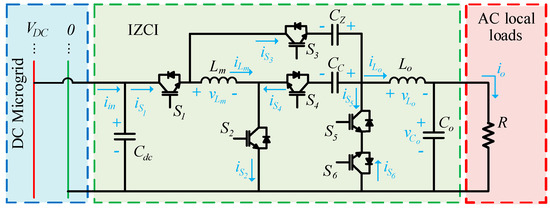
Figure 1.
The IZCI topology circuit with voltages and currents is highlighted.
The IZCI operates in DCM. In this way, the static gain maintains an approximately linear relationship with the duty cycle, facilitating the regulation of a sinusoidal reference. Moreover, this configuration reduces the influence of right-half-plane (RHP) zeros, resulting in a less complex control structure when compared to operation in continuous conduction mode (CCM), in which these zeros have a significant influence, and the static gain shows nonlinear behavior.
Figure 2 illustrates the control diagram of the AC output voltage . A PI-MR controller regulates the duty cycle of the IZCI inverter, driving the power switches. The output voltage is continuously compared to the reference voltage , defined as the product of a sinusoidal function and the reference peak voltage .
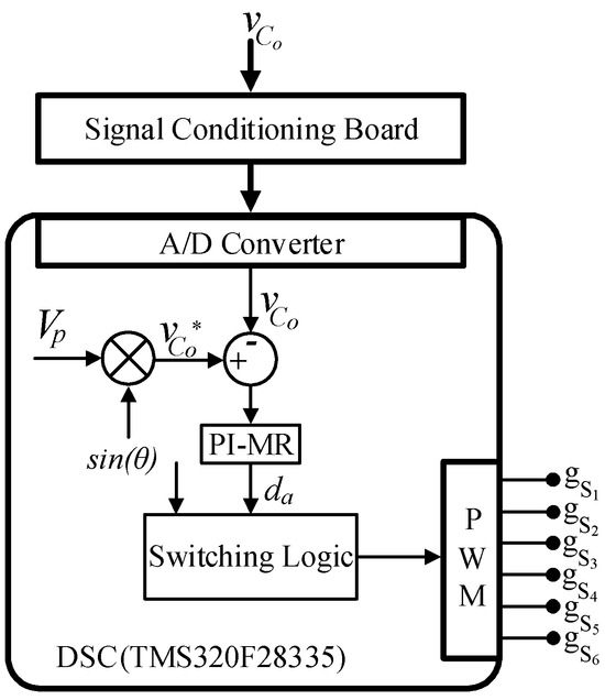
Figure 2.
IZCI control diagram.
The IZCI operates with three distinct switching stages during the positive half-cycle and three additional stages during the negative half-cycle, as shown in Figure 3 and Figure 4. To accomplish this, the topology requires six switches, where during each half-cycle of the output voltage, only one switch operates at high frequency. In contrast, the others operate at low frequency or remain inactive. Table 1 presents the corresponding switching logic.
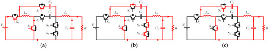
Figure 3.
Operating stages of the IZCI during the positive half-cycle: (a) first stage; (b) second stage; and (c) third stage.
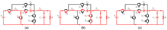
Figure 4.
Operating stages of the IZCI during the negative half-cycle: (a) first stage; (b) second stage; and (c) third stage.

Table 1.
Switching logic of the power switches.
2.1.1. IZCI—Zeta Operation Mode
In the IZCI topology, the switches , and remain always turned on during the positive half-cycle. The antiparallel diode in the switch operates as the diode of the Zeta converter. The switch connects the Zeta capacitor to the circuit.
First operating stage : In this stage, switches , , and are turned on. The inductors and are magnetized, as shown in Figure 3a. Additionally, the output inductor is magnetized according to the relationship . Assuming the equality of voltage in coupling and output capacitors, is magnetized by the input voltage only (i.e., the same voltage across the inductor ).
Second operation stage : In this stage, the switch is turned off, leading to the demagnetization of inductors and . The output inductor demagnetizes into the output capacitor and the load. According to Figure 3b, the current flows to S6 and the body diode of S5 through the capacitor Cz, inverting the current flow in this capacitor, which must present a zero average value over the switching period. As a result, during the first and third operation stages, the current flows through the switch that remains continuously on during the whole positive half-cycle, and at the second operation stage, it flows through its antiparallel diode. Figure 3b shows this interval stage operation.
Third operating stage : In this stage, illustrated in Figure 3c, the sum of currents through and reaches zero, i.e., . As a result, the diode of the switch becomes reverse-biased, and only current exchange occurs between the inductors and .
2.1.2. IZCI—Ćuk Operation Mode
During the negative half-cycle, switches , , and of the IZCI remain permanently turned on. The antiparallel diode with the switch operates as the diode of the Ćuk converter, and switch connects the Ćuk capacitor into the circuit.
First operating stage : In this stage (Figure 4a), the negative half-cycle occurs in a similar way; however, the high-frequency switch is now . Switch , which previously operated at high frequency, remains continuously turned on throughout the negative half-cycle, providing a current path for the inductor during the first stage. Inductors and are magnetized in this stage according to the relationships and . The coupling capacitor is being discharged, supplying energy to both the load and the output inductor . Considering the average voltage across the capacitor , it corresponds to the sum of the input and output voltages, resulting in . By substituting this into the output inductor voltage expression, both inductors are magnetized with the same voltage level.
Second operation stage : In this stage (Figure 4b), when the switch is turned off, the current previously stored in the inductors is finally demagnetized through the antiparallel diode of the switch .
Third operating stage : In this stage (Figure 4c), the current in the equivalent inductance between and reaches zero, that is, .
2.2. Main Waveforms of the IZCI
This section presents the main waveforms of the IZCI circuit, obtained by analyzing a switching period formed by the IZCI converter in stages , , and . The analysis also considers the converter in stages , , and , assuming ideal components to enhance understanding. As shown in Figure 5, the magnetization and demagnetization of the inductors occur during the first and second operating stages corresponding to each mode (Zeta and Ćuk), similar to traditional converters.
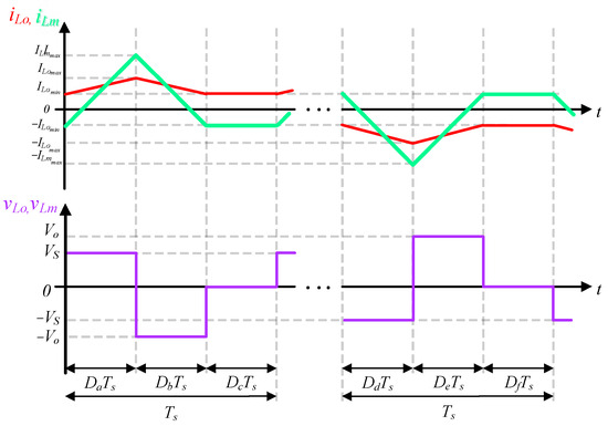
Figure 5.
Voltage and current waveforms in the inductors and .
Figure 6 presents the voltage and current waveforms across the capacitors. The analysis of the operating stages shows that the same currents flowing through the inductors also flow through the capacitors. For capacitor , during stage , it carries the same current that flows through the inductor , which is a linearly varying current with low ripple. In stage , it assumes the current flowing through the inductor , which has a higher ripple than in the previous stage, decreasing linearly until reaching a minimum value that remains constant until the end of the stage . Capacitor , in turn, receives the high-frequency alternating component of the current flowing through the inductor .
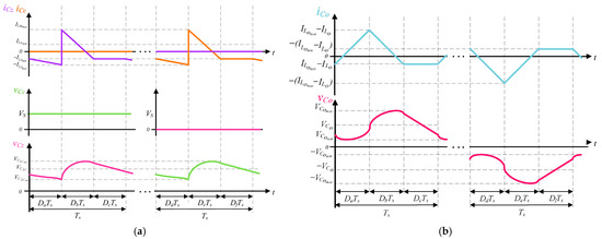
Figure 6.
Voltage and current waveforms in the capacitors: (a) Zeta and Ćuk capacitor ; (b) output capacitor .
The voltages and currents through switches S1 and S2 and the intrinsic diodes and exhibit similar behavior. Thus, only the waveforms for the switch S1 are shown in Figure 7. When the power switch operates in the Ćuk mode, the current flowing through it equals the input current, the same as the current flowing through the inductor . In the Zeta mode, the current through the switch corresponds to the sum of the currents in the inductors and . In contrast, the switch S2 presents the same current as the inductor during the positive half-cycle of the output voltage as a conventional Zeta, and during the negative half-cycle of the output voltage, the current through the switch S2 equals the sum of the current through Lm and Lo, as a conventional Ćuk converter.
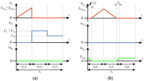
Figure 7.
Voltage and current waveforms in the semiconductors and : (a) during the positive half-cycle, and (b) during the negative half-cycle.
Switches and exhibit similar behavior, as do the intrinsic diodes and . Switch and diode operate during the positive half-cycle, where in the first stage, the switch S3 conducts. During the second stage, the current flows through the antiparallel diode . During the third stage, the current flows through switch S3. The average current through the switch S3 is null once this component is connected in series with the capacitor Cz. Meanwhile, the complementary semiconductor, S6, operates similarly during the negative half-cycle. The switches and perform the role of the diodes in Zeta and Ćuk, allowing the current to flow during the second operation stage. Figure 8 illustrates the current and voltage behavior in the main switches of the IZCI.
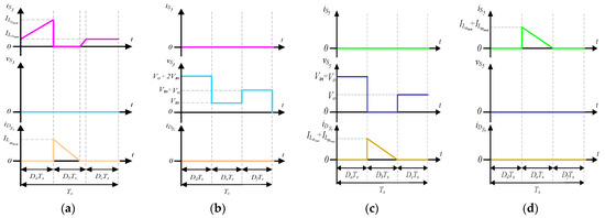
Figure 8.
Voltage and current waveforms in the semiconductors: (a) and positive half-cycle; (b) and positive half-cycle; (c) and negative half-cycle; (d) and negative half-cycle.
2.3. Static Gain
During the positive half-cycle, the IZCI operates similarly to the conventional Zeta converter in CCM. To determine the converter’s static gain, the voltage across the magnetizing inductor is analyzed in each stage, summed, and equated to zero. In the first operation stage, the voltage across the magnetizing inductor equals the input voltage. . In the second operation stage, . In the third stage, it is observed that the voltage across the inductors becomes zero, and therefore, energy is exchanged solely between them, . As a result, the average of the operational stages leads to , establishing the following relationship between the output and input voltage, as follows:
During the negative half-cycle, operating similarly to the conventional Ćuk converter in CCM, the same relationship as in the Zeta mode is obtained in the first operation stage, . In the second operation stage, . In the third stage, there is no voltage across the magnetizing inductor. As a result, the average operating stages during the negative half-cycle lead to (1).
According to [36], it is possible to consider the duty cycle for a converter operating in CCM, by relating the equivalent inductance is established based on the interaction between and , and the switching frequency , as derived in (2).
By substituting (2) into (1), resulting in (3) for the static gain of the circuit is obtained. The static gain depends on the inductances, the load, the switching frequency, and the control action.
The similar result between the average stages during the positive and negative half-cycles demonstrates the equivalence of the Zeta and Ćuk structures operating in the IZCI under DCM. According to (3), the static gain depends on factors such as the inductances, processed power, and switching frequency. The choice of these factors influences the operation mode and can provoke an unintentional CCM operation, losing the desired characteristics. The static gain depends on the power level, which limits the operation range of the topology. These dependencies and limitations are drawbacks compared to CCM converters.
2.4. Modeling and Control Design
The IZCI operates similarly to a conventional DC-DC Zeta converter during the positive half-cycle of the output voltage, presenting the same static gain, close dynamics, and similar behavior. Thus, an equivalent circuit (Figure 9) for this half-cycle can be adopted to obtain the mathematical model.
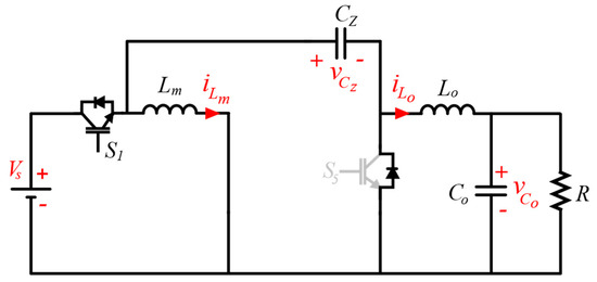
Figure 9.
Equivalent circuit for the IZCI operating during the positive half-cycle of the output voltage.
Initially, space-state averaging (SSA) was used to obtain the mathematical model of the IZCI. However, when a converter operates in DCM, errors occur in the average model due to the elevated difference between average and RMS current values in the inductors [36,37]. In [37], a method to mitigate these errors for the fourth-order converter is proposed. Thus, for the IZCI, it is possible to adopt the M matrix expressed by:
Using the matrix M represented in (4), the initial SSA is represented by:
The currents through the inductors Lm and Lo, and the voltage across the capacitors Cz and Co, are adopted as state variables. The input voltage Vs is utilized as the input to the system, and the output voltage is chosen as the system’s output. The output voltage is the same as the voltage across the capacitor Co, which is a state variable, making the output easy to obtain.
Using the IZCI equivalent circuit and multiplying the matrix M, then averaging between the three operation stages, the SSA model for the IZCI converter is obtained as follows:
During the negative half-cycle of the output voltage, the IZCI converter shows dynamics close to a Ćuk converter and can be represented by Figure 10.
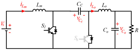
Figure 10.
An equivalent circuit for the IZCI is operating during the negative half-cycle of the output voltage.
The SSA obtained for the equivalent circuit of the IZCI for the negative half-cycle of the output voltage presents a close dynamic to that represented during the positive, exhibiting the same state matrix, Am, as derived in (7).
Ref. [36] proposed the generalized switching averaging (GSA), which divides a converter operating in DCM into two systems: the first formed by the passive elements, represented through the conventional SSA, and the other formed by the semiconductors of the topology, switches, and diodes.
The system formed by the semiconductors for the IZCI operating DCM during the positive half-cycle of the output voltage requires three gains, which are obtained as described in [37], and are exhibited as follows:
Using the SSA with the GSA, the transfer function for the IZCI, which relates the output voltage and the duty cycle, is obtained by:
where ks = [kid kvs]. The matrices Ed and Bd are obtained by the GSA and are represented as follows:
where the matrices C1, C2, and C3 represent the output matrices from the GSA for each operation stage, while the matrices E1, E2, and E3 represent the transition matrices for each operation stage, the matrix Cm is obtained by the average of the three output matrices, i.e., Cm = C1Da + C2Db + C3Dc. The matrices A1, A2, A3, C1, C2, and C3 are obtained by the SSA.
The similarity between the mathematical model is corroborated in Figure 11, which shows the open-loop frequency response for the transfer function represented by (14) and the switched equivalent circuit using the PSIM® software, version 2022. The response shows a close behavior between the mathematical model and the switching converter. Additionally, the open-loop frequency response can be used for the control design.
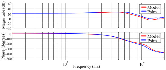
Figure 11.
Frequency response.
The transfer function (14) obtained for the IZCI enables the voltage control loop design that ensures the topology’s correct operation. The IZCI output voltage is regulated by a proportional-integral multiresonant (PI-MR) controller, implemented in a single-loop structure, which maintains a stable and regulated output voltage with a low THD. Figure 12 presents the control diagram of IZCI, where the PI-MR controller is designed following the methodology presented in [38].
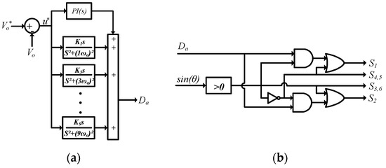
Figure 12.
Control diagrams: (a) control strategy; (b) switching logic.
3. Experimental Results
An experimental setup was built to validate the functionality of the proposed IZCI. The topology employs six power switches, IGBTs IRG4PC50UD (Infineon, Neubiberg, Germany). The three gate driver circuits, DRO100D25A (supplier, Joinville, Brazil), control the power switches. The PI-MR control is embedded into a DSP TMS320F28335. The controlled source ITC6012C-800-50 (Itech, New Taipei City Taiwan) emulates the DC microgrid. The digital oscilloscope RTH1004 (Rohde & Schwarz, Munich, Germany) obtains the main waveforms. The power quality analyzer 435-II (Fluke, Everett, WA, USA) measures the THD and calculates the system efficiency. The IZCI prototype is shown in Figure 13, while Table 2 organizes the main parameters involved in the experimental tests.
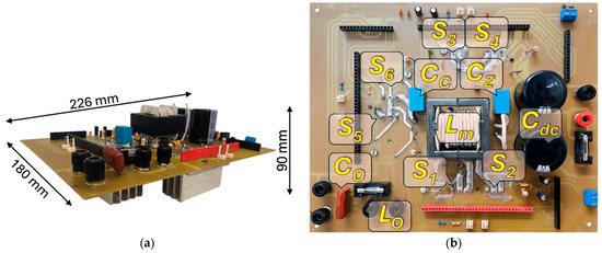
Figure 13.
PCB of experimental IZCI prototype: (a) perspective view; (b) top view.
Table 2.
Main experimental parameter for the IZCI.
Figure 14 presents the experimental output voltage and current waveforms. Initially, two resistive loads are considered: Case 1—86.4 Ω and 187 W; Case 2—57.6 Ω and 280 W, as shown in Figure 14a and Figure 14b, respectively. Subsequently, a nonlinear load is analyzed (Case 3), consisting of a 120 Ω resistive load connected in parallel with a single-phase full-bridge rectifier supplying an RC load (R3 = 250 Ω and C3 = 100 µF), totaling 264 W, as illustrated in Figure 14c. As observed, the IZCI can maintain a regulated and sinusoidal output voltage in all three evaluated cases.
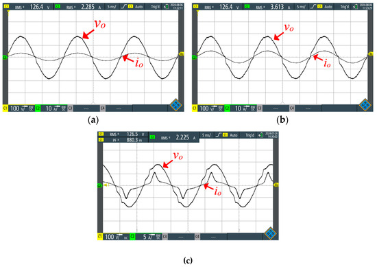
Figure 14.
Output voltage and current for: (a) Case 1; (b) Case 2; and (c) Case 3.
Figure 15a shows the dynamic result obtained when switching from load 1 to load 2, while the load step from load 2 to load 1 can be observed in Figure 15b. A slight oscillation is observed near the voltage peak during load transitions. Despite such oscillations during the load transitions, it can be seen that the controller used proved capable of readily adjusting the voltage levels.
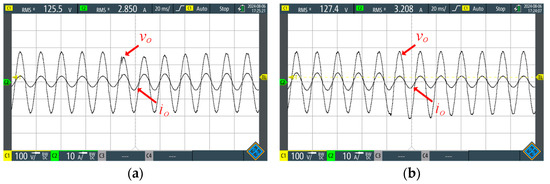
Figure 15.
Load step response: (a) from Case 1 to Case 2; and (b) from Case 2 to Case 1.
The THD of the output voltage for the resistive loads does not exceed 3%, as shown in Figure 16a and Figure 16b for Cases 1 and 2, respectively. In Case 3, the IZCI achieves an output voltage THD of 3.7% when supplying a nonlinear load with 50.8% current THD.
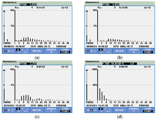
Figure 16.
Harmonic spectrum: (a) output voltage in Case 1; (b) output voltage in Case 2; (c) output voltage in Case 3; and (d) output current in Case 3.
The PI-MR controller demonstrated superior performance in reference tracking under nonlinear load conditions compared to the conventional PI controller, significantly reducing total harmonic distortion (THD). This is attributed to its resonant terms, which enhance error compensation at specific frequencies, making it well-suited for systems with periodic disturbances and harmonic rejection requirements.
The harmonic spectra of the output voltage and current for Case 3 are illustrated in Figure 16c and Figure 16d, respectively. The results confirm that the IZCI can deliver a sinusoidal output voltage with low THD for both linear and nonlinear loads.
The IZCI achieves an efficiency of approximately 90% at the nominal power. In comparison, a traditional two-stage system would require each stage to reach an efficiency of 95% to attain a similar overall performance. Furthermore, the IZCI maintains an efficiency of over 80% at power levels below 50 W. Figure 17 illustrates the IZCI efficiency using conventional silicon IGBT switching devices.
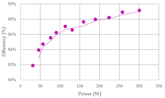
Figure 17.
Efficiency curve of IZCI topology.
The conduction and switching losses of the semiconductor devices predominantly determine the converter’s efficiency. The power variation implies changes in the current level through switches related to the transition between the turn-on and turn-off instants. DCM operation guarantees ZCS during the turn-on instant, reducing the switching losses associated, whereas the turn-off losses increase with higher power levels. On the other hand, power variation significantly affects conduction losses, as they are directly related to the RMS currents flowing through the converter. Therefore, the efficiency is lower at low power levels, since the switching losses are more considerable. The efficiency increases for a range of power, reaching the maximum value. After this point, the conduction losses became higher, mainly due to a quadratic relation with the RMS current, reducing the efficiency. The DCM operation has an intrinsic power limitation, provoking, in some cases, an efficiency curve without a conventional convex shape, as presented in topologies operating in CCM.
Table 3 presents a comparative analysis of key parameters, considering other works that address integrated inverters similar to the IZCI. The analyzed topologies exhibited nominal power ratings ranging from 147 W to 2000 W, with the configurations proposed in [32,33] standing out for operating at higher power levels of 1000 W and 2000 W, respectively. None of the examined inverters employ high-frequency transformer components that, when present, directly affect the voltage stress on the semiconductor switches due to the associated transformation ratio.
Table 3.
Comparative analysis of the IZCI with other integrated inverters.
In comparison to the works presented in [24,25,26,28,30,32,33], the IZCI exhibits a low THD for the output voltage synthesized by the converter. It can be noted that the converter proposed in [29] has a lower THD than the IZCI; however, it shows a higher rate when evaluated under a nonlinear load, reaching approximately 6.8%, compared to the previously reported 3.7%.
Another aspect to be evaluated is the output voltage in comparison to the input voltage, where once again the IZCI shows an advantage over the converters presented in [25,30,33], which were assessed in scenarios requiring voltage step-down.
4. Conclusions
This paper has proposed a novel single-phase integrated inverter topology designed for standalone applications. By combining the structural principles of the Zeta and Ćuk converters into a unified architecture, the IZCI achieves DC/AC conversion with inherent voltage step-up capability while maintaining high performance in terms of power quality and energy efficiency.
The IZCI operates by alternating between Zeta and Ćuk modes, depending on the half-cycle of the output voltage. This dual-mode behavior results in a more uniform component utilization, reduces current ripple, and mitigates stress on the power switches.
Experimental results validate the effectiveness of the proposed solution. The IZCI achieved output voltage THD levels below 4% across various loading scenarios, including nonlinear loads with significant current distortion. Furthermore, the inverter demonstrated high energy conversion efficiency, reaching approximately 90% at nominal load and maintaining over 80% under reduced power. These results highlight the IZCI’s suitability for energy-sensitive applications where power quality and efficiency are critical.
The IZCI topology is a technically viable and efficient solution for modern energy systems. Its compact design, high efficiency, low harmonic distortion, and control flexibility make it well-suited for distributed generation, UPS, and autonomous hybrid systems.
Author Contributions
Conceptualization, A.R.M.G., A.A.D., L.P.S., and S.A.O.d.S.; methodology, A.R.M.G., A.A.D., L.P.S., and S.A.O.d.S.; validation, A.R.M.G., A.A.D., Ó.P.W., L.P.S., and S.A.O.d.S.; formal analysis, A.R.M.G., A.A.D., Ó.P.W., L.P.S., and S.A.O.d.S.; investigation, A.R.M.G., A.A.D., L.P.S., and S.A.O.d.S.; writing—original draft preparation, A.R.M.G., A.A.D., Ó.P.W., L.P.S., and S.A.O.d.S.; funding acquisition and supervision, L.P.S. and S.A.O.d.S. All authors have read and agreed to the published version of the manuscript.
Funding
This research was funded by CNPq, process nº 308620/2021-6, 304948/2024-1, and 304707/2021-0. This study was financed in part by the Coordenação de Aperfeiçoamento de Pessoal de Nível Superior—Brazil (CAPES)—Finance Code 001.
Data Availability Statement
Data sharing is not applicable.
Conflicts of Interest
The authors declare no conflicts of interest.
References
- Olabi, A.; Abdelkareem, M.A. Renewable energy and climate change. Renew. Sustain. Energy Rev. 2022, 158, 112111. [Google Scholar] [CrossRef]
- Candra, O.; Chammam, A.; Alvarez, J.R.N.; Muda, I.; Aybar, H.Ş. The Impact of Renewable Energy Sources on the Sustainable Development of the Economy and Greenhouse Gas Emissions. Sustainability 2023, 15, 2104. [Google Scholar] [CrossRef]
- Rahman, A.; Farrok, O.; Haque, M. Environmental impact of renewable energy source based electrical power plants: Solar, wind, hydroelectric, biomass, geothermal, tidal, ocean, and osmotic. Renew. Sustain. Energy Rev. 2022, 161, 112279. [Google Scholar] [CrossRef]
- Ebhota, W.S.; Jen, T.-C. Fossil Fuels Environmental Challenges and the Role of Solar Photovoltaic Technology Advances in Fast Tracking Hybrid Renewable Energy System. Int. J. Precis. Eng. Manuf. Technol. 2020, 7, 97–117. [Google Scholar] [CrossRef]
- Li, X.; Sun, Y.; Liu, X.; Ming, Y.; Wu, Y. Development of a comprehensive method to estimate the optical, thermal and electrical performance of a complex PV window for building integration. Energy 2024, 294, 130251. [Google Scholar] [CrossRef]
- Muttaqi, K.M.; Islam, R.; Sutanto, D. Future Power Distribution Grids: Integration of Renewable Energy, Energy Storage, Electric Vehicles, Superconductor, and Magnetic Bus. IEEE Trans. Appl. Supercond. 2019, 29, 1–5. [Google Scholar] [CrossRef]
- Haegel, N.M.; Kurtz, S.R. Global Progress Toward Renewable Electricity: Tracking the Role of Solar (Version 2). IEEE J. Photovolt. 2022, 12, 1265–1272. [Google Scholar] [CrossRef]
- Tang, Z.; Yang, Y.; Blaabjerg, F. Power Electronics: The Enabling Technology for Renewable Energy Integration. CSEE J. Power Energy Syst. 2022, 8, 39–52. [Google Scholar] [CrossRef]
- de Assis, B.G.; Braga, E.P.C.; Nascimento, C.B.; Júnior, E.A. High-Voltage-Gain Integrated Boost SEPIC DC-DC Converter for Renewable Energy Applications. Eletrônica De Potência 2019, 24, 336–344. [Google Scholar] [CrossRef]
- Nyamathulla, S.; Chittathuru, D. A Review of Multilevel Inverter Topologies for Grid-Connected Sustainable Solar Photovoltaic Systems. Sustainability 2023, 15, 13376. [Google Scholar] [CrossRef]
- Dionizio, A.A.; Sampaio, L.P.; da Silva, S.A.O.; Monteiro, V.; Afonso, J.L. Hybrid Inverter Zeta-Ćuk for Grid-Tied Photovoltaic Applications. IEEE Open J. Power Electron. 2025, 6, 1094–1109. [Google Scholar] [CrossRef]
- Duong, T.-D.; Nguyen, M.-K.; Tran, T.-T.; Vo, D.-V.; Lim, Y.-C.; Choi, J.-H. Topology Review of Three-Phase Two-Level Transformerless Photovoltaic Inverters for Common-Mode Voltage Reduction. Energies 2022, 15, 3106. [Google Scholar] [CrossRef]
- Pires, V.F.; Pires, A.; Cordeiro, A. DC Microgrids: Benefits, Architectures, Perspectives and Challenges. Energies 2023, 16, 1217. [Google Scholar] [CrossRef]
- Sarvi, M.; Zohdi, H.Z. A comprehensive overview of DC-DC converters control methods and topologies in DC microgrids. Energy Sci. Eng. 2024, 12, 2017–2036. [Google Scholar] [CrossRef]
- Quizhpe, K.; Arévalo, P.; Ochoa-Correa, D.; Villa-Ávila, E. Optimizing Microgrid Planning for Renewable Integration in Power Systems: A Comprehensive Review. Electronics 2024, 13, 3620. [Google Scholar] [CrossRef]
- Ali, S.; Zheng, Z.; Aillerie, M.; Sawicki, J.-P.; Péra, M.-C.; Hissel, D. A Review of DC Microgrid Energy Management Systems Dedicated to Residential Applications. Energies 2021, 14, 4308. [Google Scholar] [CrossRef]
- Sahoo, S.K.; Sinha, A.K.; Kishore, N.K. Control Techniques in AC, DC, and Hybrid AC–DC Microgrid: A Review. IEEE J. Emerg. Sel. Top. Power Electron. 2018, 6, 738–759. [Google Scholar] [CrossRef]
- Adegboyega, A.W.; Sepasi, S.; Howlader, H.O.R.; Griswold, B.; Matsuura, M.; Roose, L.R. DC Microgrid Deployments and Challenges: A Comprehensive Review of Academic and Corporate Implementations. Energies 2025, 18, 1064. [Google Scholar] [CrossRef]
- Ming, W. Power Electronic Converters for Microgrids; IntechOpen: London, UK, 2021. [Google Scholar]
- Joddumahanthi, V.; Knypiński, Ł.; Gopal, Y.; Kasprzak, K. Review of Power Electronics Technologies in the Integration of Renewable Energy Systems. Appl. Sci. 2025, 15, 4523. [Google Scholar] [CrossRef]
- Schiffer, J.; Zonetti, D.; Ortega, R.; Stanković, A.M.; Sezi, T.; Raisch, J. A survey on modeling of microgrids-from fundamental physics to phasors and voltage sources. Automatica 2016, 74, 135–150. [Google Scholar] [CrossRef]
- Mathew, D.; Naidu, R.C. A review on single-phase boost inverter technology for low power grid integrated solar PV applications. Ain Shams Eng. J. 2024, 15, 102365. [Google Scholar] [CrossRef]
- Coelho, S.; Monteiro, V.; Afonso, J.L. Topological Advances in Isolated DC–DC Converters: High-Efficiency Design for Renewable Energy Integration. Sustainability 2025, 17, 2336. [Google Scholar] [CrossRef]
- Lee, S.S.; Lim, C.S.; Siwakoti, Y.P.; Lee, K.-B. Single-Stage Common-Ground Boost Inverter (S2CGBI) for Solar Photovoltaic Systems. In Proceedings of the 2019 IEEE Energy Conversion Congress and Exposition (ECCE), Baltimore, MA, USA, 29 September–3 October 2019; pp. 4229–4233. [Google Scholar]
- Lin, Z.; Su, M.; Liu, Y.; Sun, Y.; Liao, Y.; Chen, X. Single-phase integrated power decoupling inverter based on Boost converter. In Proceedings of the IEEE 9th International Power Electronics and Motion Control Conference (IPEMC2020-ECCE Asia), Nanjing, China, 29 November–2 December 2020; pp. 405–408. [Google Scholar]
- Abdeen, E.; Gaafar, M.A.; Orabi, M. Performance analysis for single-stage buck-boost inverter. In Proceedings of the International Conference on Innovative Trends in Computer Engineering (ITCE’2019), Aswan, Egypt, 2–4 February 2019; pp. 2–4. [Google Scholar]
- Paul, A.R.; Bhattacharya, A.; Chatterjee, K. A Novel SEPIC-Ćuk Based High Gain Solar Micro-Inverter for Integration to Grid. In Proceedings of the 2019 National Power Electronics Conference (NPEC), Tiruchirappalli, India, 13–15 December 2019; pp. 1–5. [Google Scholar]
- Awad, K.; Abdel-Rahim, O.; Orabi, M. A New Single-Phase Single-Stage Buck-Boost Inverter For Grid Connected PV Applications. In Proceedings of the 2019 IEEE Conference on Power Electronics and Renewable Energy (CPERE), Aswan, Egypt, 23–25 October 2019; pp. 32–37. [Google Scholar]
- Dionizio, A.A.; Pelz, G.M.; Sampaio, L.P.; da Silva, S.A.O. Novel Integrated Zeta Inverter for Standalone Applications. Energies 2024, 17, 2748. [Google Scholar] [CrossRef]
- Yue, Z. Research on single-stage Cuk inverter for photovoltaic power generation. In Proceedings of the IEEE 16th Conference on Industrial Electronics and Applications (ICIEA), Chengdu, China, 1–4 August 2021; pp. 688–694. [Google Scholar]
- Dionizio, A.A.; Sampaio, L.P.; Da Silva, S.A.O. Integrated Cuk Inverter for Single-Phase Grid-Tied Photovoltaic System. In Proceedings of the 2023 38th Conference on Design of Circuits and Integrated Systems (DCIS), Málaga, Spain, 15–17 November 2023; pp. 1–6. [Google Scholar]
- Wang, L.; Shan, M. A novel single-stage common-ground Zeta-based inverter with nonelectrolytic capacitor. IEEE Trans. Power Electron. 2022, 37, 11319–11331. [Google Scholar] [CrossRef]
- Ghosh, S.; Nathan, K.; Long, T.; Tripathi, P.; Siwakoti, Y. Single Phase Integrated Ćuk Transformerless SiC Inverter for Grid-Connected PV Systems. In Proceedings of the 2018 1st Workshop on Wide Bandgap Power Devices and Applications in Asia (WiPDA Asia), Xi’an, China, 16–28 May 2018; pp. 18–22. [Google Scholar]
- Sampaio, L.P.; da Silva, S.A.O.; Costa, P.J.S. Integrated Zeta inverter applied in a single-phase grid-connected photovoltaic system. In Proceedings of the 15th Brazilian Power Electronics Conference and 5th IEEE Southern Power Electronics Conference (COBEP/SPEC), Santos, Brazil, 1–4 December 2019; pp. 1–6. [Google Scholar]
- Inoue, R.T.; Dionizio, A.A.; Sampaio, L.P.; da Silva, S.A.O.; de Brito, M.A.G. Single-Phase Single-Stage Integrated Ćuk Inverter Operating in Discontinuous Conduction Mode for Autonomous Operation. Int. J. Circuit Theory Appl. 2025. [Google Scholar] [CrossRef]
- Erickson, R.W.; Maksimovic, D. Erickson, Fundamentals of Power Electronics, 1st ed.; Chapman & Hall: London, UK, 1984. [Google Scholar]
- Dionizio, A.A.; Sampaio, L.P.; da Silva, S.A.O. Generalized state space averaging modeling to fourth-order power converters operating in DCM. Int. J. Circuit Theory Appl. 2024, 53, 1031–1055. [Google Scholar] [CrossRef]
- Bacon, V.D.; da Silva, S.A.O.; Campanhol, L.B.G.; Angélico, B.A. Stability analysis and performance evaluation of a single-phase phase-locked loop algorithm using a non-autonomous adaptive filter. IET Power Electron. 2014, 7, 2081–2092. [Google Scholar] [CrossRef]
Disclaimer/Publisher’s Note: The statements, opinions and data contained in all publications are solely those of the individual author(s) and contributor(s) and not of MDPI and/or the editor(s). MDPI and/or the editor(s) disclaim responsibility for any injury to people or property resulting from any ideas, methods, instructions or products referred to in the content. |
© 2025 by the authors. Licensee MDPI, Basel, Switzerland. This article is an open access article distributed under the terms and conditions of the Creative Commons Attribution (CC BY) license (https://creativecommons.org/licenses/by/4.0/).