Article

Atmospheric Plasma Etching-Assisted Chemical Mechanical Polishing for 4H-SiC: Parameter Optimization and Surface Mechanism Analysis

1
College of Mechanical Engineering, Zhejiang University of Technology, Hangzhou 310023, China
2
Key Laboratory of Special Purpose Equipment and Advanced Processing Technology, Ministry of Education and Zhejiang Province, Zhejiang University of Technology, Hangzhou 310023, China
3
School of Advanced Manufacturing, Shenzhen Campus of Sun Yat-Sen University, Shenzhen 518107, China
*
Author to whom correspondence should be addressed.
Processes 2025, 13(8), 2550; https://doi.org/10.3390/pr13082550
Submission received: 2 July 2025 / Revised: 29 July 2025 / Accepted: 6 August 2025 / Published: 13 August 2025
(This article belongs to the Special Issue Processes in 2025)

Abstract

Silicon carbide (SiC) is widely utilized in semiconductors, microelectronics, optoelectronics, and other advanced technologies. However, its inherent characteristics, such as its hardness, brittleness, and high chemical stability, limit the processing efficiency and application of SiC wafers. This study explores the use of plasma etching as a pre-treatment step before chemical mechanical polishing (CMP) to enhance the material removal rate and improve CMP efficiency. Experiments were designed based on the Taguchi method to investigate the etching rate of plasma under various processing parameters, including applied power, nozzle-to-substrate distance, and etching time. The experimental results indicate that the etching rate is directly proportional to the applied power and increases with nozzle-to-substrate distance within 3–5 mm, while it is independent of etching time. A maximum etching rate of 5.99 μm/min is achieved under optimal conditions. And the etching mechanism and microstructural changes in SiC during plasma etching were analyzed using X-ray photoelectron spectroscopy (XPS), scanning electron microscopy (SEM), white light interferometry, and ultra-depth-of-field microscopy. XPS confirmed the formation of a softened SiO2 layer, which reduces hardness and enhances CMP efficiency; SEM revealed that etching pits form in relation to distance; and white light interferometry demonstrated that etching causes a smooth surface to become rough. Additionally, surface defects resulting from the etching process were analyzed to reveal the underlying reaction mechanism.

1. Introduction

As one of the most representative third-generation semiconductor materials, silicon carbide (SiC) is considered an ideal choice for high-temperature and high-frequency optoelectronic devices due to its wide band gap, high critical breakdown electric field, and high thermal conductivity [1,2,3]. However, the extremely high hardness (Mohs hardness 9.5, second only to diamond) and chemical inertness of SiC single crystal also make it a typical difficult-to-machine material [4,5]. The combination of ultra-high hardness and chemical stability limits the use of soft abrasive polishing methods, while hard abrasive polishing techniques inevitably introduce subsurface damage [6]. The quality of the SiC substrate directly affects the quality of epitaxial materials, device reliability, and lifespan [7,8,9]. Achieving efficient material removal and polishing methods for SiC with both high efficiency and excellent surface quality is therefore essential.
Chemical mechanical polishing (CMP) is a technique that combines chemical and mechanical actions to achieve material removal [10,11,12]. Compared to traditional polishing methods, CMP effectively removes surface defects, enhances surface quality, and offers low processing costs. As a result, it is widely used and has become one of the most common methods for processing SiC wafers [13,14,15]. However, due to the high hardness and excellent chemical stability of SiC, achieving a high material removal rate (MRR) while maintaining an ultra-smooth surface quality is challenging [16,17]. To improve the polishing efficiency and quality of traditional CMP, many researchers have proposed or utilized synergistic technology to assist CMP, aiming for the high-efficiency, high-quality, and low-damage polishing of SiC. Deng et al. [18] utilized an electrolytic/polishing solution containing CeO2 abrasive particles to process single-crystal SiC through electrochemical mechanical polishing (ECMP). The combination of electrochemical anodizing and soft abrasive mechanical polishing ultimately results in a polished surface with a high-quality finish. Building on ECMP, Yang et al. [19,20] proposed a slurryless ECMP method and applied it to the 4H-SiC (0001) surface. In this process, the oxide layer is removed using a fixed abrasive instead of a slurry. Finally, an MRR of approximately 23 μm/h and a surface roughness Sq of 1.352 nm were achieved. Yamamura et al. [21,22] proposed a novel processing technology that combines atmospheric plasma irradiation modification with the removal of soft mold materials, such as cerium oxide, known as plasma-assisted polishing (PAP). This method results in a scratch-free silicon carbide surface with a roughness of less than 0.3 nm, without introducing subsurface damage. Building on this, Deng et al. [23,24] investigated the atomic-scale planarization mechanism of silicon carbide materials in the PAP process, characterized the oxidation reaction during plasma-assisted polishing of silicon carbide, and optimized the PAP process for 4H-SiC. Although PAP technology replaces the use of strong oxidizing agents for plasma irradiation modification of the silicon carbide surface in conventional CMP, which can effectively reduce environmental pollution caused by the polishing process, the material removal rate in plasma-assisted polishing of silicon carbide is limited by the slower rate of plasma irradiation modification [25]. As a result, the lower material removal rate of PAP technology has been a key factor restricting its further development and application in the field of silicon carbide polishing [26].
Some scholars have also proposed new techniques to replace CMP. Zhang et al. [27,28] introduced an atmospheric pressure plasma polishing (APPP) method, which uses atmospheric pressure plasma to generate a large number of highly reactive atoms. These atoms promote material removal through chemical reactions between the reactive atoms and the surface atoms of the workpiece. Yamamura et al. [29] proposed plasma chemical vapor phase processing (PCVM), a non-contact chemical processing technique that removes material through chemical reactions without applying mechanical loads to the workpiece, thus preventing the formation of subsurface damage (SSD) during the material removal process. However, both of these etching methods have limited planarization capabilities at the atomic level.
To address the issues mentioned above, this study employs atmospheric plasma etching as a pre-treatment process for CMP. The study innovatively proposes atmospheric pressure plasma etching as a pre-treatment step for CMP, achieving targeted removal of SSD through non-contact gas phase reactions, which differs from the simultaneous action mechanisms of traditional PAP and ECMP. However, improper process parameters during the etching process can lead to a decline in both the etching rate and surface quality. While existing research on SiC plasma etching primarily focuses on processing efficiency, the formation mechanisms of surface defects (such as focal spots and etch pits) and their control methods remain insufficiently explored. Furthermore, there is limited research on the impact of irradiation parameters on the surface quality of the workpieces. In this paper, the Taguchi method is applied for the first time to optimize plasma etching parameters, while the chemical mechanisms underlying the etching reaction are investigated using XPS, SEM, and other analytical techniques.

2. Experimental Design and Methodology

2.1. Plasma Etching Assisted CMP Model

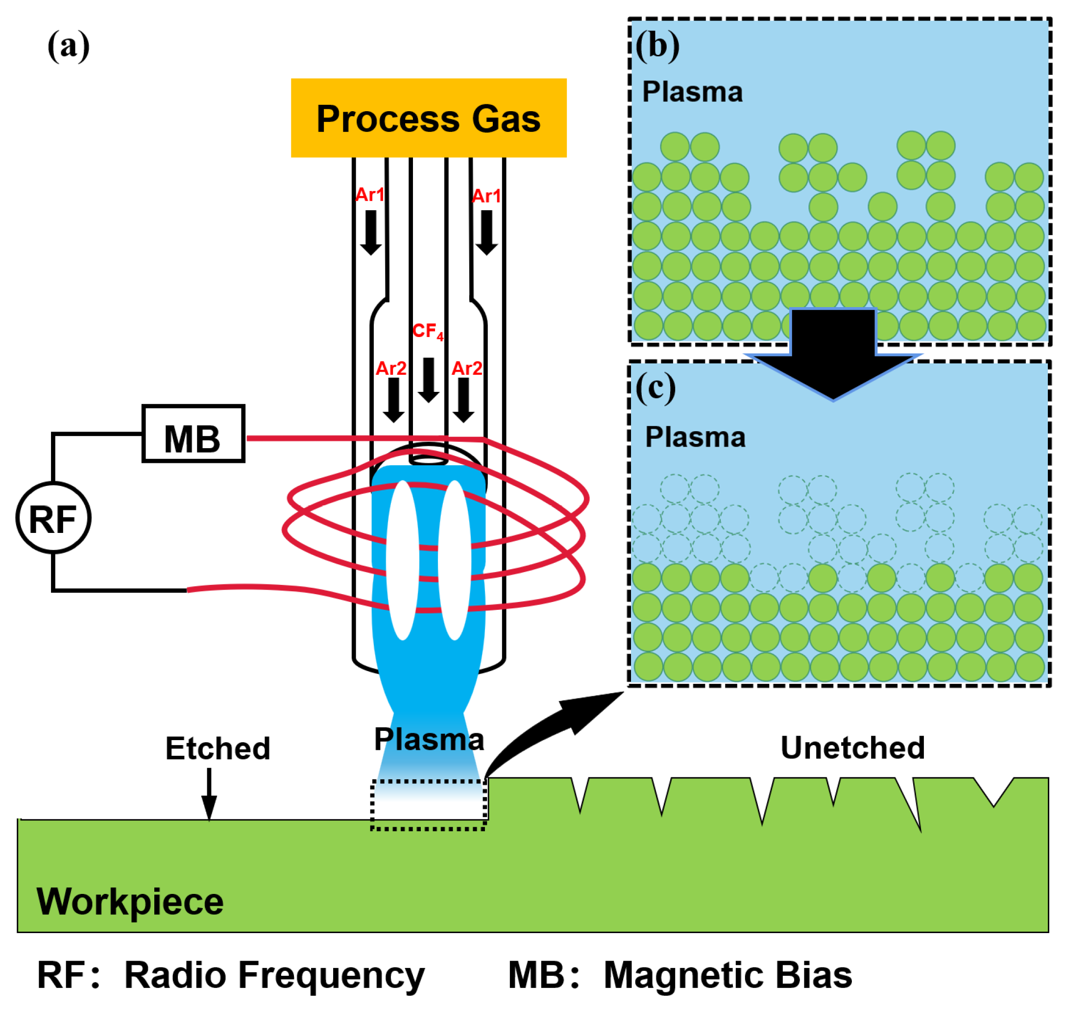
This study integrates plasma etching with CMP to achieve effective, non-destructive material removal and surface polishing. Plasma etching not only removes surface cracks but also changes the subsurface structure through oxidation. The plasma etching-assisted CMP technology not only facilitates an efficient material removal rate through plasma etching and eliminates the SSD generated during early processing but also employs CMP to remove reactants deposited on the surface, enhancing the workpiece’s surface quality. This combined etching and polishing method fully leverages atmospheric plasma etching to efficiently remove surface material, improving the polishing efficiency of the CMP process and enabling non-destructive fine polishing of the SiC material surface. The mechanism of the plasma etching-assisted CMP process is illustrated in Figure 1.

2.2. Plasma Etching Principle

The essence of plasma etching of SiC involves a chemical reaction between active particles generated in a glow discharge and the material to be processed. The principle of plasma etching of SiC wafers is illustrated in Figure 2. Argon is introduced into the ceramic tube of the plasma generator’s outer layer as the carrier gas. Argon atoms are ionized into Ar+ ions and electrons, forming argon plasma. Simultaneously, CF4 is introduced from the gas inlet of the central layer as the reaction gas. This reaction gas is excited within the plasma and ionized by the plasma generator to form a plasma. The plasma is then directed onto the surface of the workpiece via the plasma torch. Additionally, part of the oxygen in the atmosphere is ionized into oxygen plasma by the plasma generator, and a chemical reaction occurs on the surface of the workpiece. Plasma etching does not reduce the surface roughness of the workpiece; rather, it quantitatively removes the convex portions of the material’s surface, thereby flattening the surface and forming an amorphous layer in the processed area. Compared to the SiC wafer, the amorphous layer has lower hardness and reduced polishing difficulty, which can significantly shorten processing time and enhance the CMP efficiency of the wafer.

2.3. Experimental Process and Conditions

The etching experiment was conducted using an atmospheric plasma jet system. Prior to starting the experiment, the discharge gas (Ar) was introduced to purge impurities from the reaction chamber. Then, the reaction gas, CF4, was introduced to ignite the system and power it up, producing a visible blue plasma. The fixture position was adjusted using the control panel, and the workpiece to be processed was manually placed and fixed onto the vacuum suction fixture. The fixture position was then fine-tuned, and tool setting was performed. Once the tool setting was complete, the running program was written in the control panel according to the experimental plan. The properties of the SiC wafer are presented in Table 1, and the workpiece dimensions are 20 × 20 mm. Prior to the experiment, the samples were cleaned by immersion in hydrofluoric (HF) to remove the original oxide layer.
The experimental conditions are summarized in Table 2. Based on prior research, both the applied power and processing distance are constrained within specific ranges. The applied power is set between 400 and 550 W. This range is chosen because, at lower power levels, the etching effect is insufficient, while at higher power levels, the surface temperature of the workpiece becomes excessively high, leading to thermal stress that can cause the wafer to break. To prevent uneven heating of the wafer surface, which could lead to cracks or fractures, the processing distance is carefully controlled. If the distance is too small, the wafer heats unevenly, but if it is too large, the plasma gas struggles to make full contact with the workpiece surface, impairing the etching reaction. Therefore, the processing distance is limited to the range of 3–6 mm.
Power, time, and distance are the primary process parameters that influence the etching depth and etching rate of SiC wafers. This study investigates the effects of varying applied power, etching time, and nozzle-to-substrate distance on the Si surface processing of SiC wafers. Each factor is evaluated at four levels, with equal intervals. A Taguchi design experiment was created using Minitab19 software, and the L16 (43) orthogonal array was selected, as shown in Table 3. The etching rate was used as the response variable, and Minitab19 software was employed to visually analyze the experimental data.

2.4. Characterization and Testing

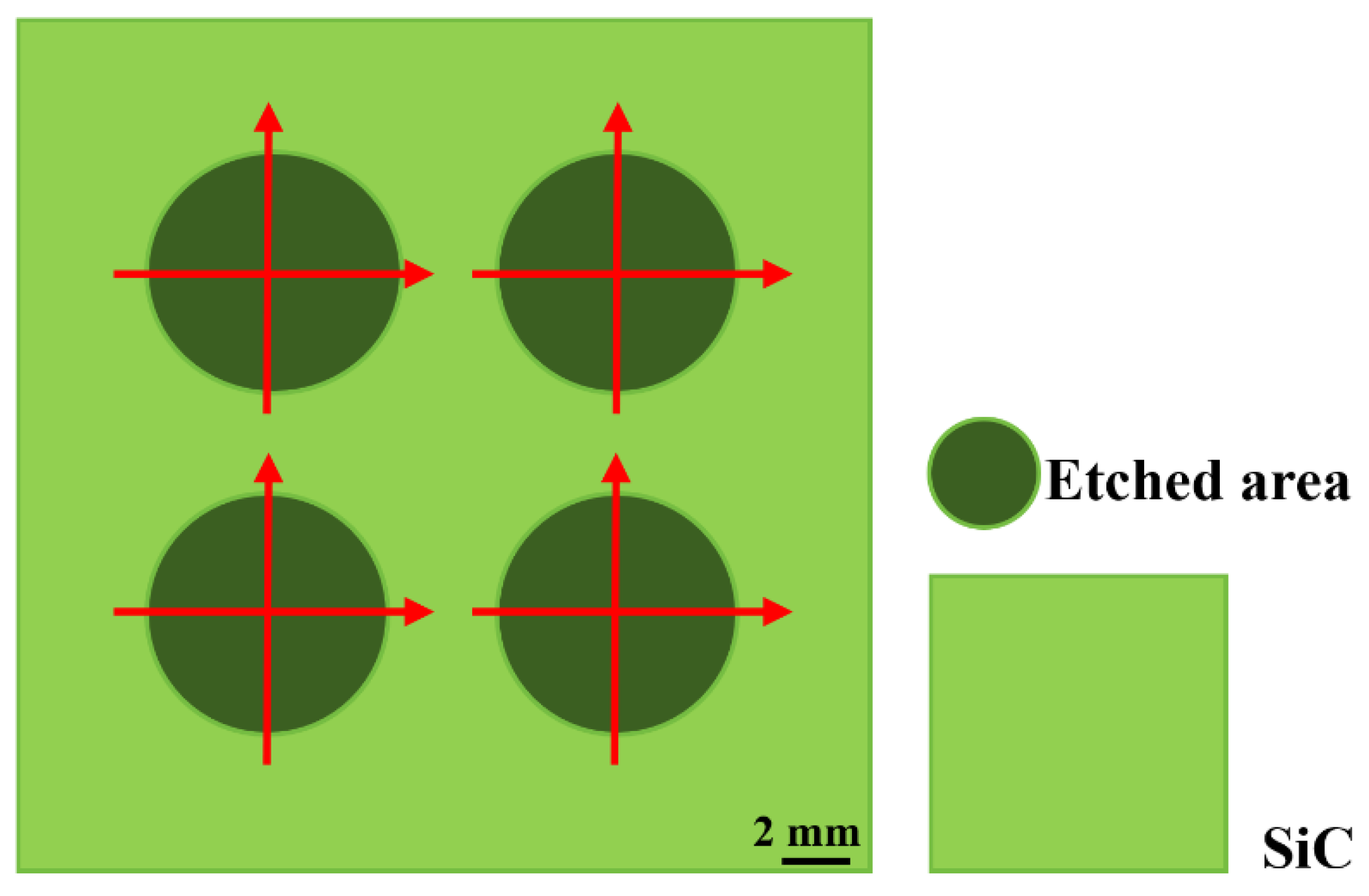
At the end of the single-point etching experiments, the cross-sectional profiles of the material removal areas were measured using a profilometer (Talysurf i-Series, Taylor Hobson, Leicester, UK). As shown in Figure 3, contour measurements were taken along the x- and y-axis directions for each etched area, and the average material removal depths along the two main axes were recorded for different parameter configurations. The evolution of the surface topography before and after etching was then comparatively analyzed using scanning white-light interferometry (SWLI; Super View W1, Chotest, Shenzhen, China), super-depth-of-field microscopy (UDFM; VHX-7000, KEYENCE, Osaka, Japan), and scanning electron microscopy (SEM; SU8010, HITACHI, Tokyo, Japan).

3. Results and Discussion

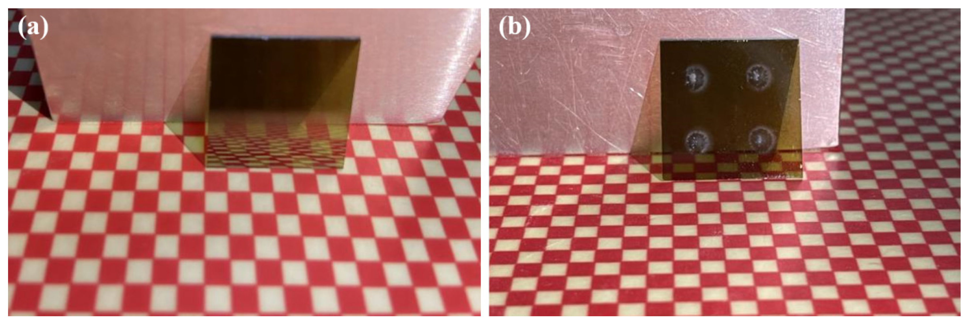
The images of 4H-SiC before and after plasma etching are shown in Figure 4. It is clearly observed that a white deposition has formed within the etching area.
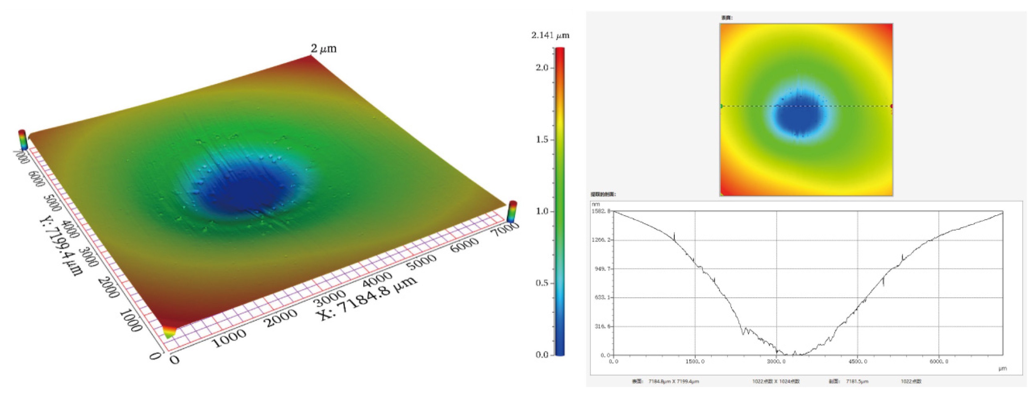
The profiles of the etched areas were measured and analyzed using a SWLI, with the results presented in Figure 5. The etched area profiles exhibit a Gaussian distribution, with etching depth indicated by markers. This suggests that during the plasma etching of SiC, the center of the plasma torch has the highest ion density, while the outer ring has the weakest ion density, resulting in a Gaussian energy distribution overall.
Etching   rate = Maximum   depth t

3.1. Effect of Etching Parameters on Etching Rate

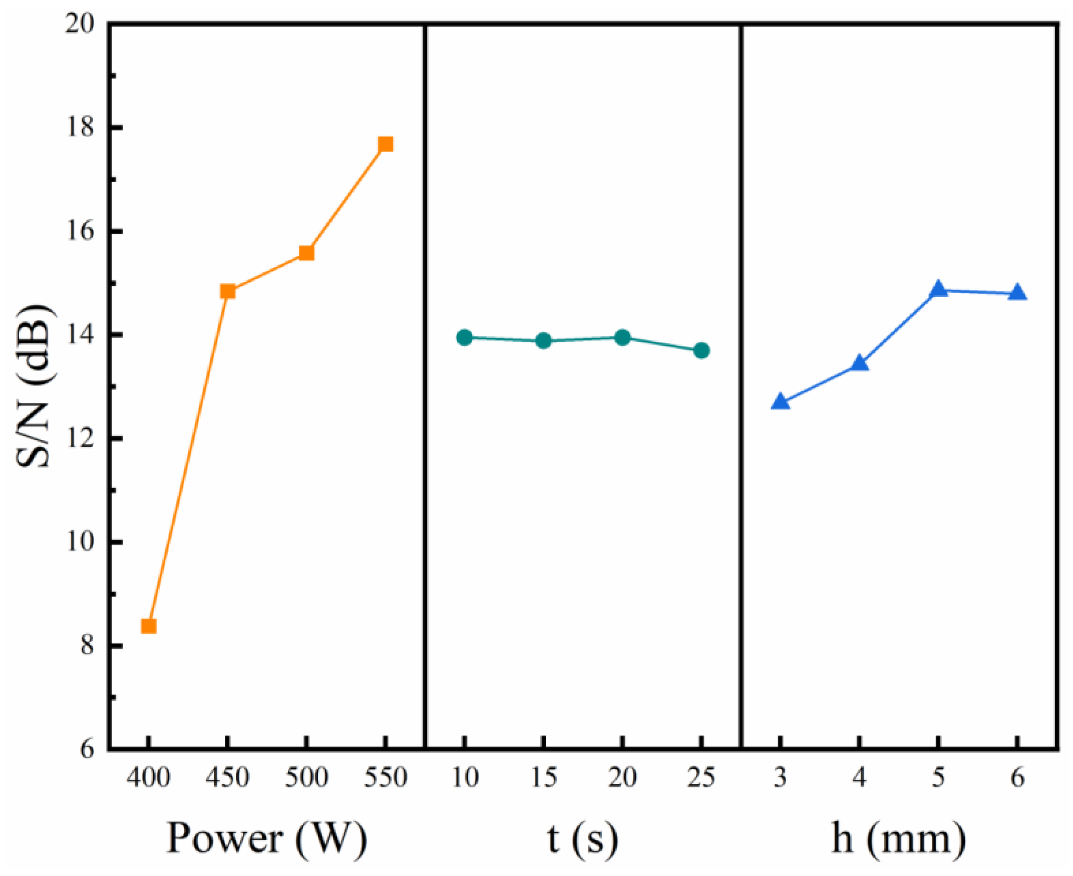
The etching rate and S/N values calculated from the experiment are presented in Table 4 and Table 5. The variation curve of the average S/N response for the etching rate is shown in Figure 6.
As shown in Figure 6, the S/N value of the etching rate increases with increasing applied power. According to the etching principle, the etching process is a chemical reaction between SiC and the plasma of the reaction gas. On one hand, as the applied power increases, plasma activity increases, and the concentration of plasma generated by ionization collisions rises, leading to an increase in the reaction rate during the etching process. On the other hand, as the applied power rises, the temperature of the plasma increases, which, in turn, increases the energy of the reactant molecules. This causes some of the initially low-energy molecules to become activated molecules, thereby increasing the number of activated molecules among the reactants. The frequency of effective collisions increases, which accelerates the chemical reaction rate and thus boosts the etching rate.
As shown in Figure 6, the etching rate remains relatively constant for a period of time as the processing time increases, indicating that processing time has little effect on the etching rate. However, the etching depth is positively correlated with the processing time.
In Figure 6, the S/N value of the etching rate increases as the processing distance increases within the range of 3–5 mm. As the processing distance increases, the oxygen concentration in direct contact with the workpiece surface rises, which, in turn, increases the reaction rate during the etching process and enhances the etching rate. When the processing distance exceeds 5 mm, the S/N value of the etching rate decreases as the distance increases. At larger distances, the plasma gas concentration decreases, the surface temperature of the workpiece decreases, and the energy of the reactant molecules is reduced, leading to a slower chemical reaction rate and a corresponding decrease in the etching rate.
In summary, the optimal process parameters are 550 W and 5 mm. Processing for 25 s under these parameters yields a steady-state etching rate of 5.99 μm/min.

3.2. Effect of Etching Parameters on Surface Quality

3.2.1. Effect of Distance

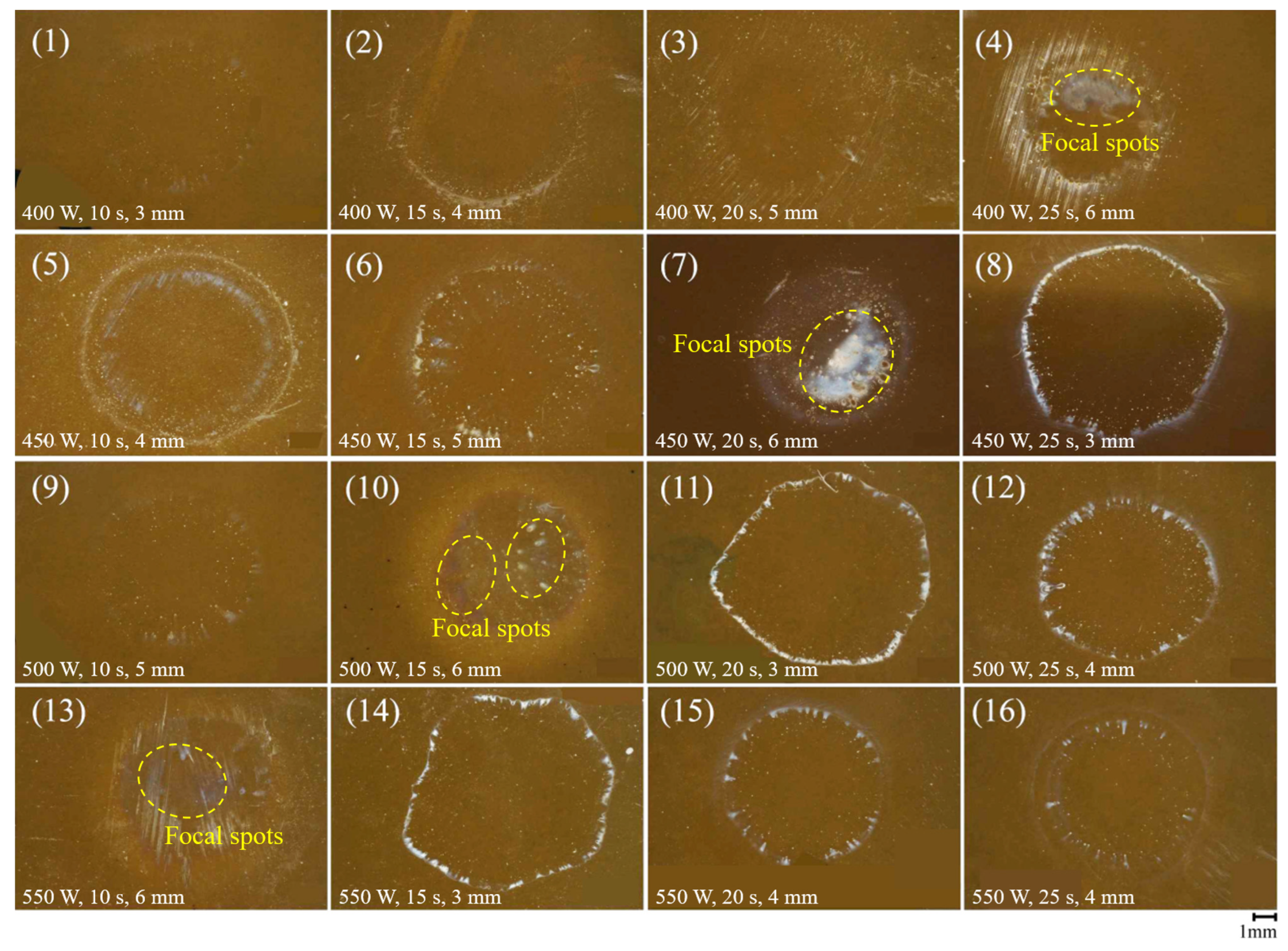
The entire etched area of 16 sample groups was examined using UDFM, and two-dimensional surface images of the etched regions were captured, as shown in Figure 7. It was observed that flaky focal spots appeared on the surface of the samples in groups 4, 7, 10, and 13, while no focal spots were found in the etched areas of the other groups. The formation of focal spots on the workpiece surface can interfere with the subsequent plasma–surface reactions, thereby affecting the efficiency of plasma etching. This observation aligns with the results of the etching rate signal-to-noise ratio. The presence of focal spots deteriorates the surface quality of the workpiece, which contradicts the original goal of processing silicon carbide. Therefore, preventing the formation of focal spots during the etching process is crucial.
To investigate the cause of the focal spots, the experimental parameters of these four groups of samples were analyzed. It was found that the experimental distance parameter (h = 6 mm) was the same across all four groups, while other parameters varied.
As shown in Figure 7, when the processing distance is between 3 and 5 mm, the etched area is smooth, and no focal spots are observed. However, at a processing distance of 6 mm, dotted deposition impurities and large focal spots appear in the etched area. Based on the principles of etching, it can be concluded that the presence of focal spots is due to incomplete reactions during the plasma etching process.

3.2.2. Effect of Temperature

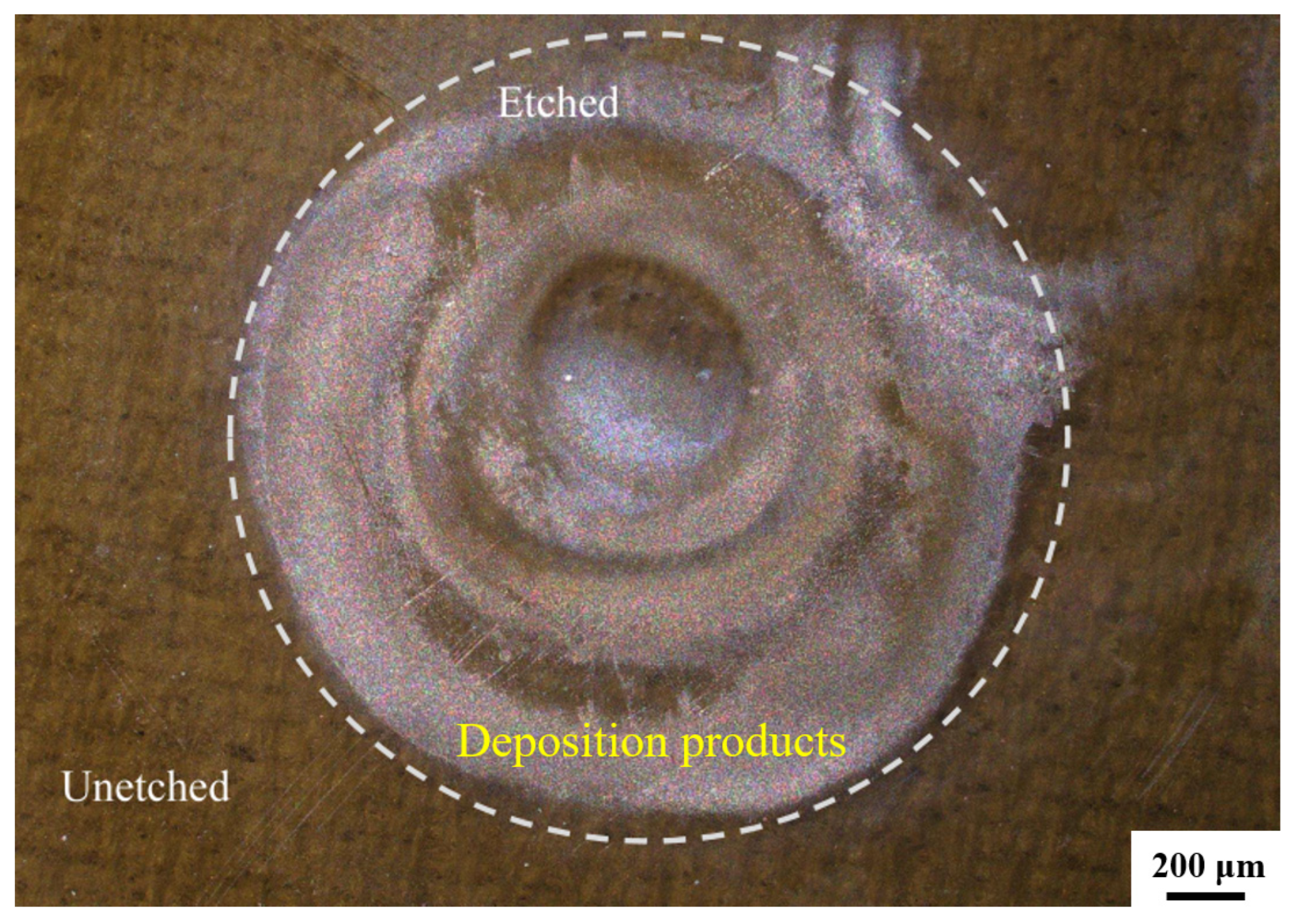
Currently, there are still some challenges in pure plasma etching experiments. While plasma etching of SiC can achieve a high MRR, deposition products on the wafer surface degrade its smoothness, as shown in Figure 8. To determine whether these deposited products affect subsequent CMP, further investigation into their composition and formation mechanism is necessary.
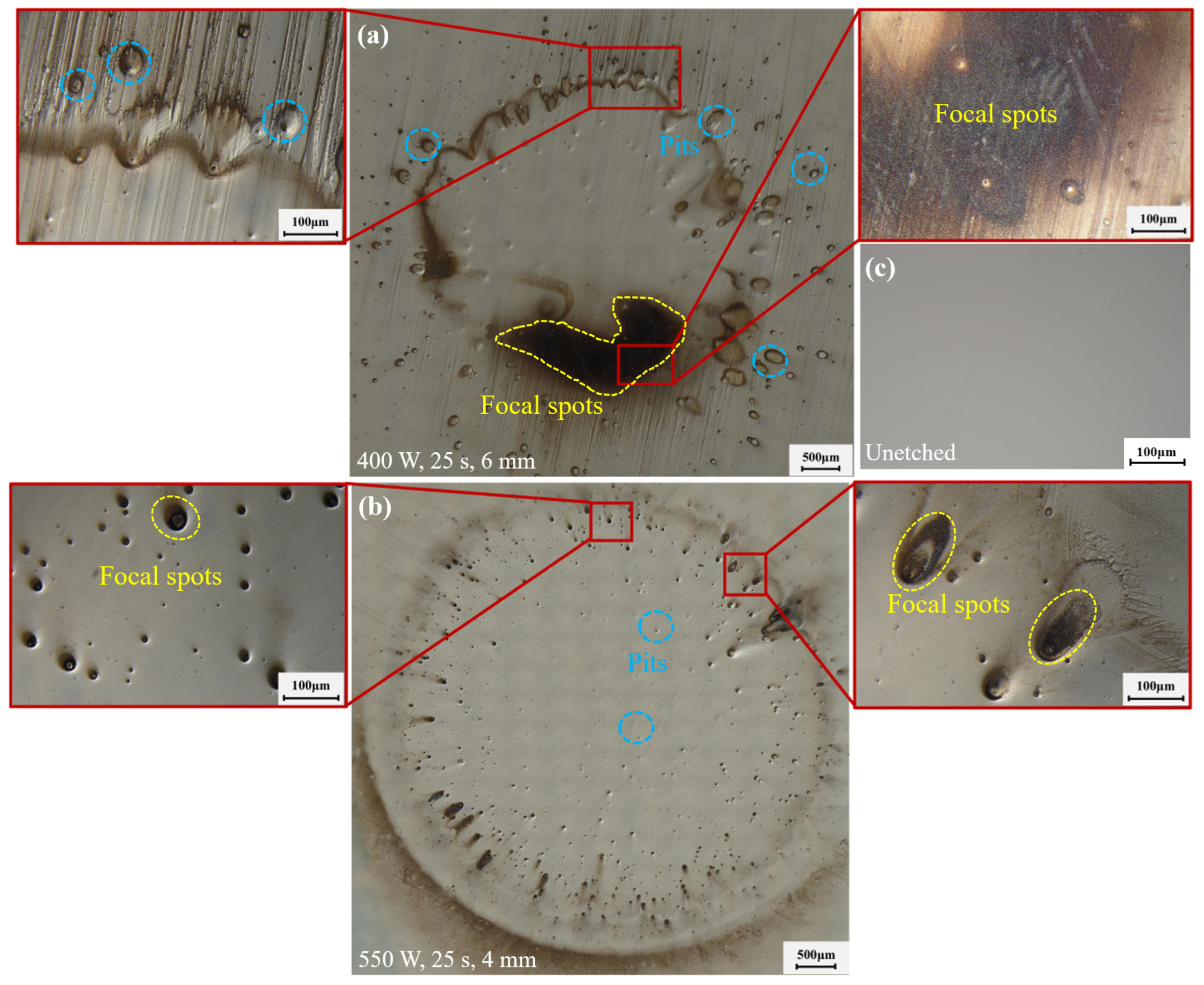
Samples processed under different parameters were analyzed using an UDFM. It was found that the surface quality of the samples varied significantly depending on the processing parameters. Some samples exhibited large focal spots, dense punctate pits, and uneven distribution, as shown in Figure 9. The presence of etching pits directly impacts the subsequent CMP process. Therefore, it is essential to analyze the causes of these etching pits to prevent their formation during the etching process.
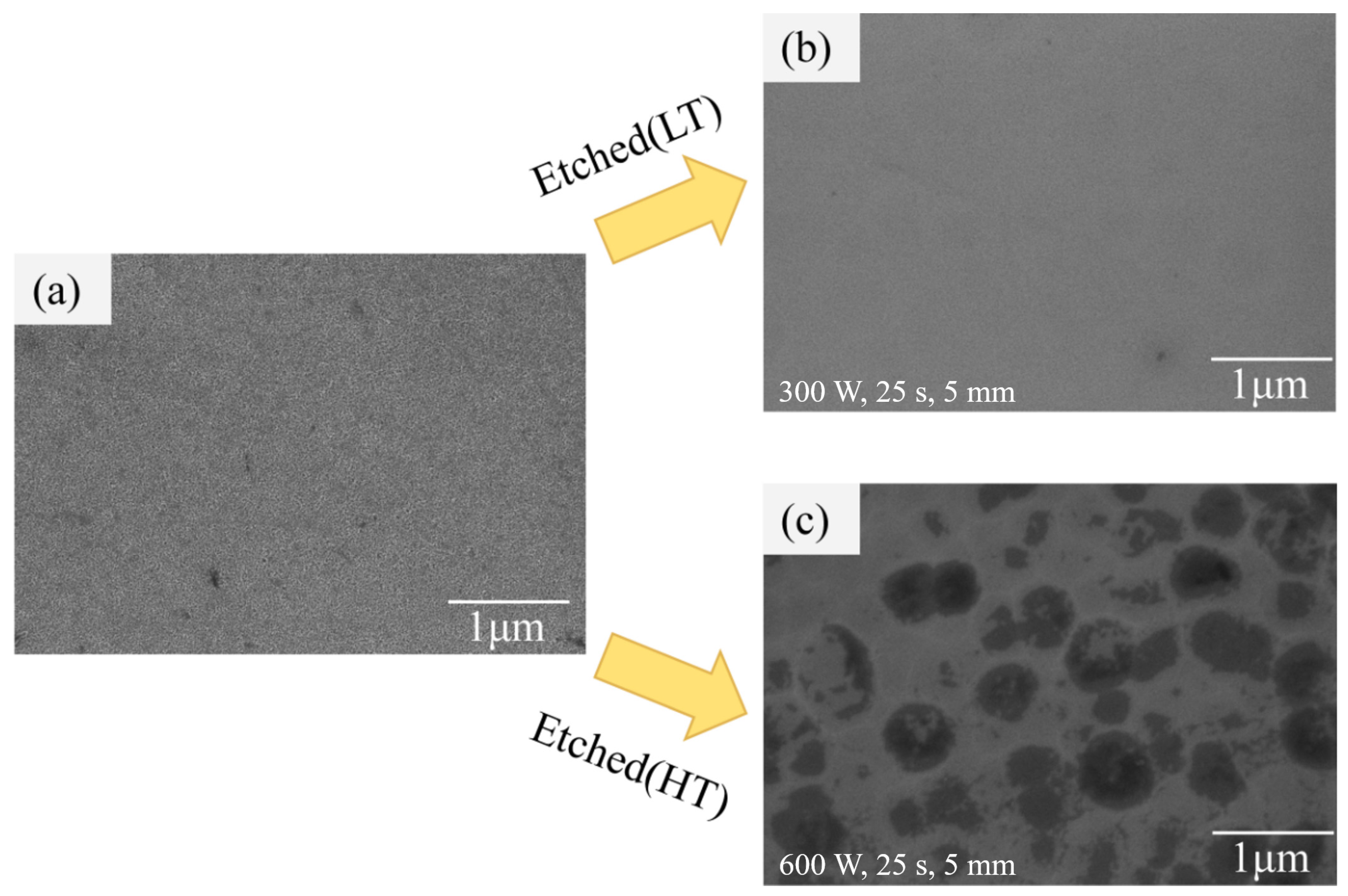
The micro-morphology of different sample groups was analyzed using an UDFM. It was observed that etching pits appeared on the surface of high-power etched samples, while low-power etched samples do not have etching pits; instead, they show burn spots formed due to insufficient etching reaction caused by excessive distance. Since etching power directly influences the plasma temperature during the etching process, to investigate whether the formation of pore structures is related to temperature, two regions of the same sample were etched with temperature as a variable. The experiment was divided into two parts: low-temperature (LT) etching and high-temperature (HT) etching. The LT range was <200 °C, and the HT range was 400–500 °C. The temperature was controlled by adjusting the power. In LT etching, the sample was etched directly by plasma without preheating, whereas in HT etching, the sample was preheated before etching.
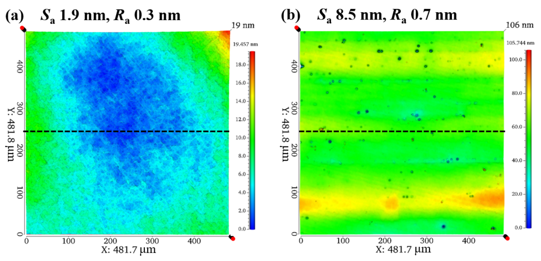
To explore the relationship between the formation of etching pits and temperature, the microstructure of the LT-etched and HT-etched regions of the sample was observed using SEM and SWLI, as shown in Figure 10 and Figure 11.
As shown in Figure 10, the micro-morphology of the etched area of the irradiated samples at different temperatures was observed using SEM. It was found that the low-temperature etched samples exhibited almost no hole-like structures, whereas the high-temperature etched samples showed dense hole-like structures in the processed area. This indicates that the formation of dense hole-like structures during the etching process is related to the processing temperature. As shown in Figure 11, a SWLI was used to measure the surface roughness of the etched area of the irradiated samples at different temperatures. The test results revealed that the surface quality of the workpiece after plasma etching was poor. However, after low-temperature etching, the surface quality was better compared to high-temperature etching, with no etched pits formed. The surface of the workpiece remained relatively flat, suggesting that the etching temperature significantly affects the surface quality of the workpiece.

3.2.3. Analysis of XPS Test Results

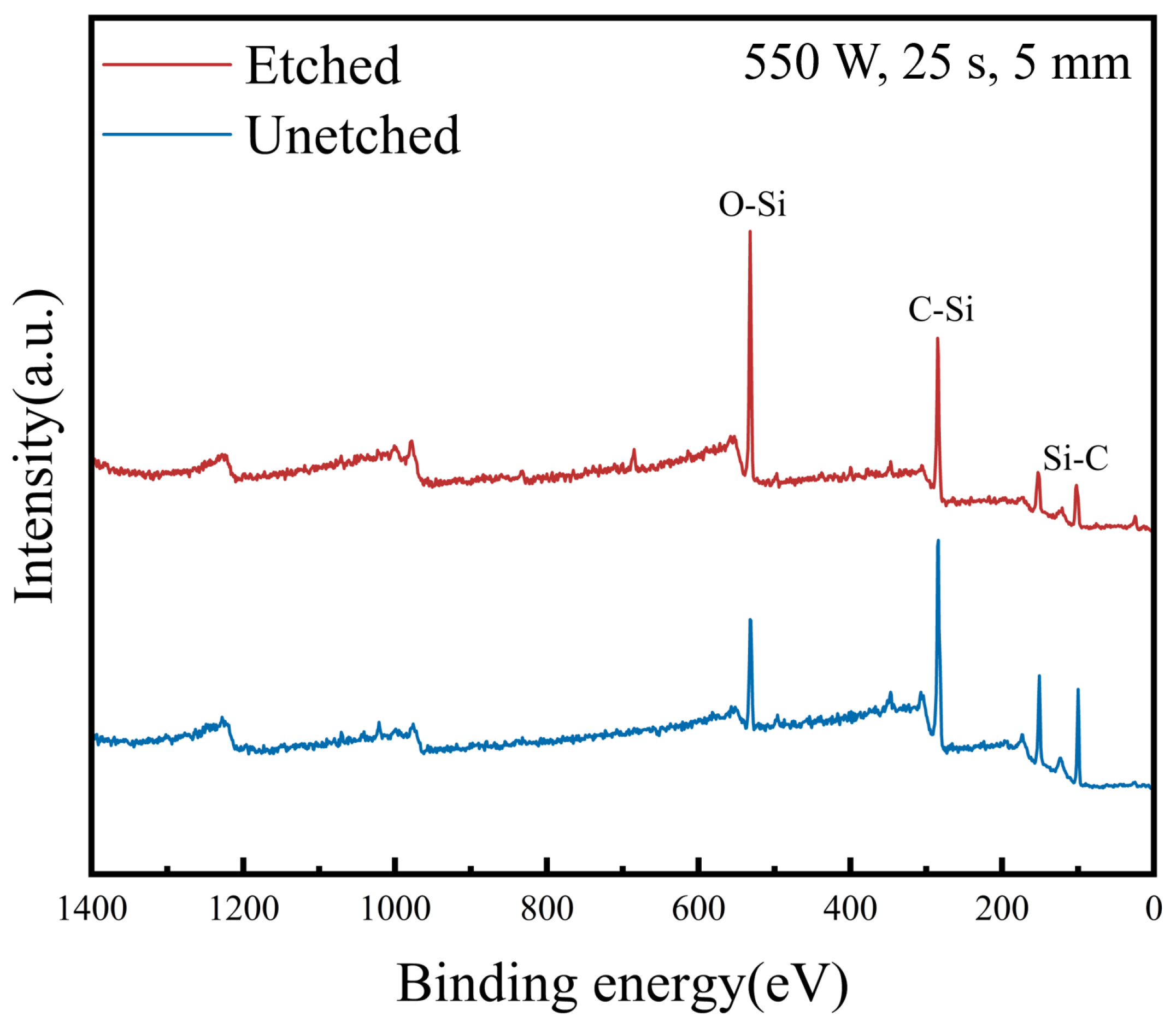
X-ray photoelectron spectroscopy (XPS; Shimadzu-KRA, TOS, Japan) was employed to investigate the microscopic chemical composition of SiC before and after irradiation. Qualitative analysis was performed by combining energy spectrum fitting and valence band spectrum analysis, as shown in Figure 12.
For this experiment, the X-ray source employed was radiographic Al Kα radiation, with aluminum as the target material (E = 1486.6 eV). The target current was set to 3 mA, the target voltage to 15 kV, and the power to 45 W. The system operated at a vacuum pressure better than 10−8 Torr, typically ranging between 4 × 10⁻⁹ Torr and 1 × 10⁻⁸ Torr. The binding energy reference was taken from the C1s peak of the C-C bond, with a correction value of 284.8 eV. Elemental binding energies were then fitted using XPSPEAK41 software.
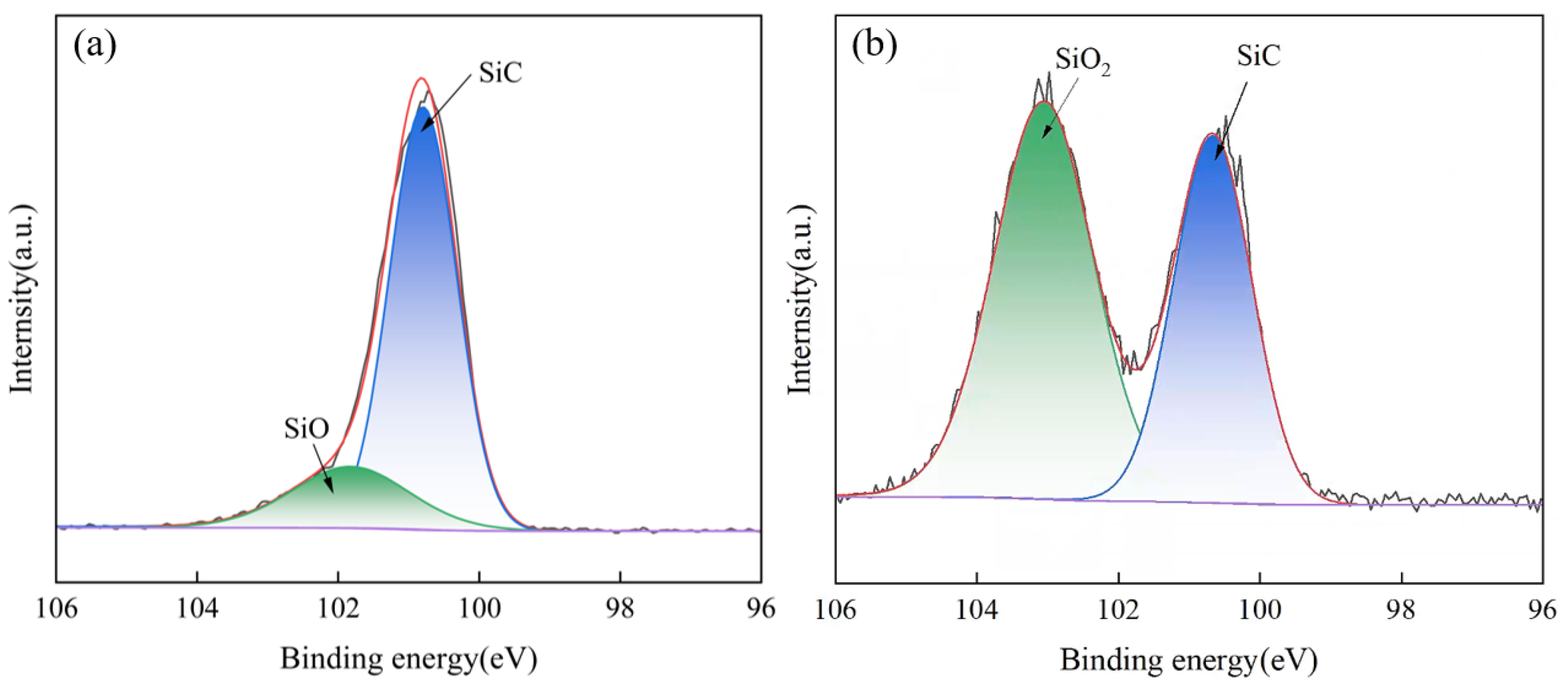
To investigate the binding state of atoms in the sample before and after irradiation, the XPS spectrum was analyzed using fine spectrum analysis, and the sample’s detection was performed through peak fitting. The XPS fine spectra of the SiC samples, both before and after irradiation, are shown in Figure 13. In the XPS analysis diagram, the purple line represents the baseline, which is used to define the peak position and determine the peak area; the black line is the drawing line of the original measurement data; the red line is the graph line fitted after adding the corresponding peak; the green and blue regions correspond to the peak areas of SiO2 and SiC before and after etching, respectively.
To quantitatively analyze the changes in the elements of SiC before and after irradiation, the specific measured values are presented in Table 6.
XPS was used to investigate the relevant reaction mechanisms and qualitatively analyze the changes in surface element composition before and after irradiation. Figure 13 shows the peak separation results of the Si2p narrow scan spectrum before and after plasma irradiation, providing insights into the transformations occurring during the plasma irradiation stage. Clearly, the untreated workpiece surface has a thin natural oxide layer, as shown in Figure 13a. Subsequently, as shown in Figure 13b, after irradiation, the Si-O bond content increases, indicating that the free Si ions, produced from the fracture of Si-C bonds due to irradiation, combine with O ions from ionization to form SiO2, which is deposited on the surface of the sample. The reaction is shown in Equation (2). In addition, trace amounts of F remain in the unetched samples, which may be due to the use of HF cleaning.
SiC + CF 4 + O 2 SiF 4 + CO 2 + SiO 2

3.3. CMP Surface Quality Verification

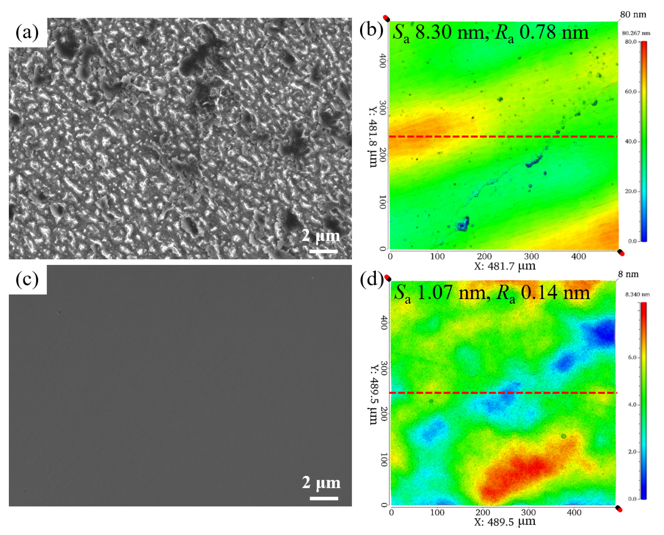
After standard CMP processing, SEM and SWLI were used to examine the microstructure and surface roughness of the polished surface, with the results shown in Figure 14. The SEM results indicate that the deposits on the etched surface were completely removed after CMP processing, leaving the surface smooth. A comparison of the SWLI test results shows that the surface roughness was significantly reduced from 0.78 nm after etching to approximately 0.14 nm.

4. Conclusions

This study proposes a novel atmospheric plasma etching-assisted CMP process for silicon carbide materials, addressing the major limitations of traditional polishing processes through three key innovations:
  • This study reveals the influence of processing parameters on plasma etching technology: the applied power provides energy for plasma ionization and affects the surface quality after etching by influencing the temperature, while the distance between the nozzle and the substrate determines the uniformity of oxidation.
  • The optimal etching process was determined through Taguchi experiments, and under optimal process conditions (550 W, 6 mm), atmospheric pressure plasma achieved the highest etching rate (5.99 μm/min) on SiC.
  • XPS analysis indicated that the products of the etching reaction were SiO2. The current process cannot completely suppress defects such as deposition and etching pits. Future research will focus on suppressing the formation of deposition and etching pits to achieve smooth surface etching technology.

Author Contributions

M.S.: investigation, validation, writing—original draft, writing–review and editing. M.W.: investigation. X.L.: investigation. J.Y.: supervision. W.H.: resources, methodology. Y.H.: supervision, funding acquisition. All authors have read and agreed to the published version of the manuscript.

Funding

This study received funding support from the National Key Research and Development Program of China (2023YFE0202900), the National Natural Science Foundation of China (52375468, 52275467).

Data Availability Statement

The data presented in this study are available on request from the corresponding author.

Conflicts of Interest

The authors declare no conflicts of interest.

References

  1. Shen, M.; Wu, L.; Wei, M.; Chen, H.; Yuan, J.; Lyu, B.; Deng, H.; To, S.; Beri, T.H.; Hang, W. High-efficiency free-damage electrochemical shear-thickening polishing of single-crystal silicon carbide. J. Manuf. Process. 2024, 132, 532–543. [Google Scholar] [CrossRef]
  2. Shen, M.; Wei, M.; Wu, L.; Han, Y.; Hong, B.; Lyu, B.; Chen, H.; Hang, W. Dominant parameters and mechanisms influencing the electrochemical shear-thickening polishing of 4H-SiC. Ceram. Int. 2024, 51, 10351–10364. [Google Scholar] [CrossRef]
  3. Lebedev, A.A. Development and Investigation of SiC and SiC-Based Devices. Crystals 2020, 10, 1127. [Google Scholar] [CrossRef]
  4. Chen, X.; Yang, X.; Xie, X.; Peng, Y.; Xiao, L.; Shao, C.; Li, H.; Hu, X.; Xu, X. Research progress of large size SiC single crystal materials and devices. Light-Sci. Appl. 2023, 12, 28. [Google Scholar] [CrossRef]
  5. Chen, Z.; Zhao, Y. Investigation into electrochemical oxidation behavior of 4H-SiC with varying anodizing conditions. Electrochem. Commun. 2019, 109, 106608. [Google Scholar] [CrossRef]
  6. Chen, H.; Wu, Z.; Hong, B.; Hang, W.; Zhang, P.; Cao, X.; Xu, Q.; Chen, P.; Chen, H.; Yuan, J.; et al. Study on the affecting factors of material removal mechanism and damage behavior of shear rheological polishing of single crystal silicon carbide. J. Manuf. Process. 2024, 112, 225–237. [Google Scholar] [CrossRef]
  7. Li, G.F.; Hang, W.; Chen, H.Y.; Wang, R.; Pi, X.; Yang, D.; Yuan, J. Effect of subsurface damages in seed crystals on the crystal quality of 4H-SiC single crystals grown by the PVT technology. Crystengcomm 2024, 26, 875–880. [Google Scholar] [CrossRef]
  8. Shen, M.; Wei, M.; Wu, L.; Hong, B.; Ye, J.; Chen, H.; Yuan, J.; Lyu, B.; Wang, C.; Deng, H.; et al. Microwave plasma modification-assisted shear-thickening polishing of single-crystal silicon carbide. Precis. Eng.-J. Int. Soc. Precis. Eng. Nanotechnol. 2025, 94, 13–25. [Google Scholar] [CrossRef]
  9. Chen, H.; Wan, H.; Hong, B.; Hang, W.; Zhu, T.; Zhang, P.; Cao, X.; Xu, Q.; Wang, R.; Han, X.; et al. A novel liquid film shearing polishing technique for silicon carbide and its processing damage mechanisms. Appl. Surf. Sci. 2025, 688, 162317. [Google Scholar] [CrossRef]
  10. Deng, J.; Lu, J.; Yan, Q.; Pan, J. Enhancement mechanism of chemical mechanical polishing for single-crystal 6H-SiC based on Electro-Fenton reaction. Diam. Relat. Mat. 2021, 111, 108147. [Google Scholar] [CrossRef]
  11. Pang, L.F.; Li, X.B.; Li, T.T.; Jia, J.P. Ultra Precision Chemical Mechanical Polishing Technology for SiC Wafer. Micronano-Electron. Technol. 2021, 58, 1035–1040. [Google Scholar] [CrossRef]
  12. Lee, H.; Kim, H.; Jeong, H. Approaches to Sustainability in Chemical Mechanical Polishing (CMP): A Review. Int. J. Precis. Eng. Manuf.-Green Technol. 2022, 9, 349–367. [Google Scholar] [CrossRef]
  13. Hang, W.; Shen, M.; Wei, M.; Wu, L.; Wang, Y.; Chen, H.; Lyu, B.; Zhao, J. Electrochemical shear-thickening polishing of 4H-SiC (000–1): Factors influencing the anodization process. Ceram. Int. 2025; in press. [Google Scholar] [CrossRef]
  14. Zhao, J.; Xu, X.; Li, W.; Hang, W. Material removal modes and processing mechanism in microultrasonic machining of ball ceramic tool. Ceram. Int. 2024, 50, 28844–28856. [Google Scholar] [CrossRef]
  15. Xu, H.; Wang, J.; Li, Q.; Pan, F. Research progress of chemical mechanical polishing technology of silicon carbide wafer. Mod. Manuf. Eng. 2022, 501, 153–161+116. [Google Scholar] [CrossRef]
  16. Lei, H.; Luo, J.; Ma, J. Advances and Problems on Chemical Mechanical Polishing. Lubr. Eng. 2002, 27, 73–76. [Google Scholar]
  17. Deng, J.; Pan, J.; Zhang, Q.; Guo, X.; Yan, Q. Research progress in chemical mechanical polishing of single crystal SiC substrates. Diam. Abras. Eng. 2020, 40, 79–91. [Google Scholar] [CrossRef]
  18. Deng, H.; Hosoya, K.; Imanishi, Y.; Endo, K.; Yamamura, K. Electro-chemical mechanical polishing of single-crystal SiC using CeO2 slurry. Electrochem. Commun. 2015, 52, 5–8. [Google Scholar] [CrossRef]
  19. Yang, X.; Yang, X.; Kawai, K.; Arima, K.; Yamamura, K. Highly efficient planarization of sliced 4H–SiC (0001) wafer by slurryless electrochemical mechanical polishing. Int. J. Mach. Tools Manuf. 2019, 144, 103431. [Google Scholar] [CrossRef]
  20. Yang, X.; Yang, X.; Kawai, K.; Arima, K.; Yamamura, K. Dominant factors and their action mechanisms on material removal rate in electrochemical mechanical polishing of 4H-SiC (0001) surface. Appl. Surf. Sci. 2021, 562, 150130. [Google Scholar] [CrossRef]
  21. Yamamura, K.; Takiguchi, T.; Ueda, M.; Deng, H.; Hattori, A.; Zettsu, N. Plasma assisted polishing of single crystal SiC for obtaining atomically flat strain-free surface. CIRP Ann.-Manuf. Technol. 2011, 60, 571–574. [Google Scholar] [CrossRef]
  22. Yamamura, K.; Takiguchi, T.; Ueda, M.; Hattori, A.N.; Zettsu, N. High-Integrity Finishing of 4H-SiC (0001) by Plasma-Assisted Polishing. Adv. Mater. Res. 2010, 126–128, 423–428. [Google Scholar] [CrossRef]
  23. Deng, H.; Endo, K.; Yamamura, K. Damage-free finishing of CVD-SiC by a combination of dry plasma etching and plasma-assisted polishing. Int. J. Mach. Tools Manuf. 2017, 115, 38–46. [Google Scholar] [CrossRef]
  24. Deng, H.; Yamamura, K. Atomic-scale flattening mechanism of 4H-SiC (0 0 0 1) in plasma assisted polishing. CIRP Ann.-Manuf. Technol. 2013, 62, 575–578. [Google Scholar] [CrossRef]
  25. Zhang, Y.; Zhang, L.; Chen, K.; Liu, D.; Lu, D.; Deng, H. Rapid subsurface damage detection of SiC using inductivity coupled plasma. Int. J. Extreme Manuf. 2021, 3, 035202. [Google Scholar] [CrossRef]
  26. Deng, H.; Endo, K.; Yamamura, K. Comparison of thermal oxidation and plasma oxidation of 4H-SiC (0001) for surface flattening. Appl. Phys. Lett. 2014, 104, 101608. [Google Scholar] [CrossRef]
  27. Zhang, J.F.; Wang, B.; Dong, S. Analysis of factors impacting atmospheric pressure plasma polishing. Int. J. Precis. Eng. Manuf. 2008, 9, 39–43. [Google Scholar]
  28. Wang, B.; Zhang, J.F.; Dong, S. New development of atmospheric pressure plasma polishing. Chin. Opt. Lett. 2009, 7, 537–538. [Google Scholar] [CrossRef]
  29. Yamamura, K.; Shimada, S.; Mori, Y. Damage-free improvement of thickness uniformity of quartz crystal wafer by plasma chemical vaporization machining. CIRP Ann.-Manuf. Technol. 2008, 57, 567–570. [Google Scholar] [CrossRef]
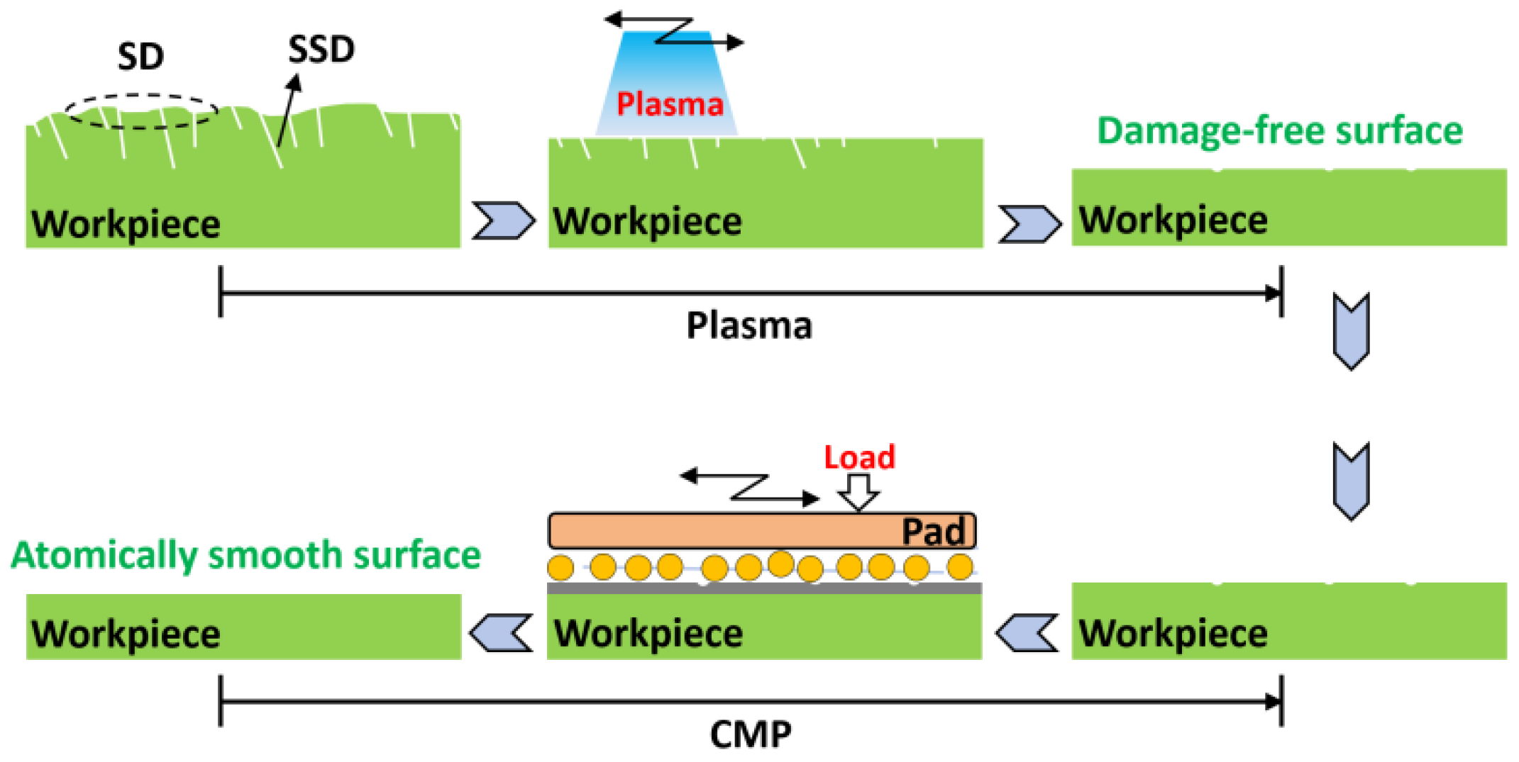
Figure 1. Schematic diagram of plasma etching-assisted CMP.
Processes 13 02550 g001
Figure 2. (a) Schematic illustration of plasma etching; (b) schematic diagram of the microstructure before processing; (c) schematic diagram of the microstructure after processing.
Processes 13 02550 g002
Figure 3. Observation line diagram of workpiece surface.
Processes 13 02550 g003
Figure 4. Surface images of the workpiece: (a) original surface, (b) processed surface.
Processes 13 02550 g004
Figure 5. Etched area morphology and profile curves.
Processes 13 02550 g005
Figure 6. S/N value of etching rate.
Processes 13 02550 g006
Figure 7. UDFM images of samples after 16 sets of experiments.
Processes 13 02550 g007
Figure 8. UDFM image of the deposition after plasma etching.
Processes 13 02550 g008
Figure 9. Etched area defect detection: (a) focal spot; (b) point etched pits; (c) unetched.
Processes 13 02550 g009
Figure 10. SEM morphology of workpiece surface: (a) not etched; (b) low-temperature etched; (c) high-temperature etched.
Processes 13 02550 g010
Figure 11. SWLI morphology: (a) low-temperature etched; (b) high-temperature etched.
Processes 13 02550 g011
Figure 12. XPS spectra of SiC samples before and after etching.
Processes 13 02550 g012
Figure 13. Si2p spectra of SiC surface (a) before and (b) after irradiation.
Processes 13 02550 g013
Figure 14. SEM and SWLI detection results: (a) SEM image of deposits after etching; (b) SWLI image of deposits after etching; (c) SEM image after polishing; (d) SWLI image after polishing.
Processes 13 02550 g014
Table 1. Material properties of SiC wafer.
ParameterValue
Density (g · cm3)3.2
melting point (°C)2700.0
Mohs Hardness9.5
Poisson ratio ν0.14
Table 2. Experimental conditions.
ParameterValue
Ar1 (slm)17
Ar2 (slm)2
CF4 (sccm)30
Power (W)400, 450, 500, 550
Time (s)10, 15, 20, 25
Distance (mm)3, 4, 5, 6
Table 3. Factor level table.
LevelFactor
ABC
P/Wt/sh/mm
1400103
2450154
3500205
4550256
Table 4. The results of the orthogonal experiment.
No.ABCDepth
/μm
Standard Deviation
Etching Rate
/(μm/min)
No.ABCDepth
/μm
Standard Deviation
Etching Rate
/(μm/min)
Power
/W
t/sh/mmPower
/W
t/sh/mm
14001030.2584 0.0389 1.5501 95001051.0727 0.09986.4364
24001540.4690 0.0730 1.8758 105001561.4510 0.16745.8040
34002051.3310 0.1603 3.9929 115002031.9477 0.23035.8432
44002561.7081 0.2081 4.0995 125002542.5646 0.29806.1549
54501041.1714 0.1547 7.0284 135501061.4776 0.16338.8658
64501551.6498 0.1922 6.5991 145501532.1180 0.20798.4721
74502061.4567 0.1109 4.3700 155502042.0296 0.11416.0887
84502531.9133 0.2230 4.5918 165502553.3809 0.32108.1142
Table 5. S/N value calculation results.
LevelAverage Etching Rate/(μm/min)
Power/Wt/sh/mm
18.37613.94912.684
214.83813.88213.425
315.57513.94714.86
417.67813.69314.794
Delta9.3020.2562.176
Rank132
Table 6. SiC element content before and after irradiation.
ElementNot Etched (%)Etched (%)
C55.0242.21
O14.2130.35
Si30.2624.26
F0.513.18
Disclaimer/Publisher’s Note: The statements, opinions and data contained in all publications are solely those of the individual author(s) and contributor(s) and not of MDPI and/or the editor(s). MDPI and/or the editor(s) disclaim responsibility for any injury to people or property resulting from any ideas, methods, instructions or products referred to in the content.