Article

Accurate and Efficient Process Modeling and Inverse Optimization for Trench Metal Oxide Semiconductor Field Effect Transistors: A Machine Learning Proxy Approach

1
College of Integrated Circuits, Zhejiang University, Hangzhou 311200, China
2
Zhejiang ICsprout Semiconductor Co., Ltd., Hangzhou 311200, China
*
Authors to whom correspondence should be addressed.
Processes 2025, 13(5), 1544; https://doi.org/10.3390/pr13051544
Submission received: 31 March 2025 / Revised: 13 May 2025 / Accepted: 15 May 2025 / Published: 16 May 2025
(This article belongs to the Special Issue Machine Learning Optimization of Chemical Processes)

Abstract

:
This study proposes a novel framework integrating long short-term memory (LSTM) networks with Bayesian optimization (BO) to address process–device co-optimization challenges in trench-gate metal–oxide–semiconductor field-effect transistor (MOSFET) manufacturing. Conventional TCAD simulations, while accurate, suffer from computational inefficiency in high-dimensional parameter spaces. To overcome this, an LSTM-based TCAD proxy model is developed, leveraging hierarchical temporal dependencies to predict electrical parameters (e.g., breakdown voltage, threshold voltage) with deviations below 3.5% compared to physical simulations. The model, validated on both N-type and P-type 20 V trench MOS devices, outperforms conventional RNN and GRU architectures, reducing average relative errors by 1.78% through its gated memory mechanism. A BO-driven inverse optimization methodology is further introduced to navigate trade-offs between conflicting objectives (e.g., minimizing on-resistance while maximizing breakdown voltage), achieving recipe predictions with a maximum deviation of 8.3% from experimental data. Validation via TCAD-simulated extrapolation tests and SEM metrology confirms the framework’s robustness under extended operating ranges (e.g., 0–40 V drain voltage) and dimensional tolerances within industrial specifications. The proposed approach establishes a scalable, data-driven paradigm for semiconductor manufacturing, effectively bridging TCAD simulations with production realities while minimizing empirical trial-and-error iterations.

1. Introduction

Trench-gate metal–oxide–semiconductor field-effect transistors (TG-MOSFETs) have emerged as pivotal components in modern power electronics, driving advancements in renewable energy systems, electric vehicles, and high-efficiency power converters [1,2]. Their vertical trench architecture offers significant advantages over planar designs. These include reduced specific on-resistance (Ron) and enhanced switching efficiency, which are critical for high-frequency operations [3,4]. However, conventional trench MOSFETs are constrained by intrinsic limitations such as high reverse recovery charge (Qrr) and switching losses associated with their body diode, which degrade performance in fast-switching applications [5,6]. To address these challenges, recent innovations have focused on integrating Schottky barrier diodes (SBDs) into trench structures, creating hybrid architectures like the SBD-TG-NMOS which aim to bypass parasitic effects and improve conduction efficiency [7,8]. Despite these advancements, optimizing the fabrication process—spanning etch uniformity, doping gradients, and thermal management—remains a multi-dimensional challenge, particularly for balancing conflicting objectives such as breakdown voltage (BV) and Ron [9,10].
Traditional technology computer-aided design (TCAD) simulations have been widely adopted to predict device performance by solving physical equations governing carrier transport and electrostatics [11,12,13]. However, their computational inefficiency becomes prohibitive in high-dimensional parameter spaces, such as those involving multi-process variables (e.g., ion-implantation dose, gate oxide thickness, and annealing time) [14,15,16]. This limitation hinders iterative design exploration and real-time process calibration, both of which are essential for industrial-scale manufacturing. Machine learning (ML) approaches [17,18], particularly recurrent neural networks (RNNs), have shown promise in modeling sequential fabrication steps by leveraging temporal dependencies in process data [19,20,21]. Yet, conventional RNNs struggle with long-term dependency capture due to vanishing gradients and fixed memory states, limiting their applicability to complex multi-step semiconductor processes [22]. Long short-term memory (LSTM) networks, with their gated architecture, overcome these limitations by adaptively retaining critical temporal information across extended sequences, making them suitable for modeling nonlinear process–device relationships [23,24,25]. Despite their potential, the application of LSTMs to trench MOSFET process optimization, particularly for co-optimizing BV and Ron, remains underexplored.
Recent advances in Bayesian optimization (BO) have demonstrated its efficacy in navigating high-dimensional design spaces, especially for multi-objective problems common in semiconductor manufacturing [26,27]. BO’s probabilistic framework, combined with Gaussian process regression, enables efficient exploration of trade-offs between conflicting objectives, such as maximizing BV while minimizing Ron. However, integrating BO with LSTM-based surrogate models to bridge TCAD simulations and fabrication realities has not been systematically investigated, particularly for N-type and P-type trench MOS devices with asymmetric doping profiles and carrier mobility effects. Existing studies often focus on isolated aspects of process optimization, neglecting the holistic interplay between sequential fabrication steps and terminal device performance [28]. This gap underscores the need for a unified framework capable of addressing both device types while maintaining alignment with industrial requirements.
To address these challenges, this study proposes a co-optimization framework combining LSTM-based TCAD proxy modeling with BO-driven inverse optimization. The LSTM model hierarchically encodes nonlinear relationships between sequential process parameters (e.g., trench depth, doping concentration) and electrical responses, while the BO methodology identifies optimal process recipes to balance BV–Ron trade-offs. Validated on 20 V N-type and P-type trench MOS devices, this framework bridges the divide between physical simulations and high-volume manufacturing, offering a scalable solution for rapid process adaptation.
The remainder of this paper is organized as follows: Section 2 details the structural design and TCAD-validated fabrication process flow of trench MOSFETs, emphasizing critical steps such as gate oxidation and ion implantation. Section 3 introduces the LSTM proxy model architecture and its integration with BO for multi-objective optimization. Section 4 validates the framework through TCAD simulations and experimental metrology. Section 5 summarizes the conclusions of this study.

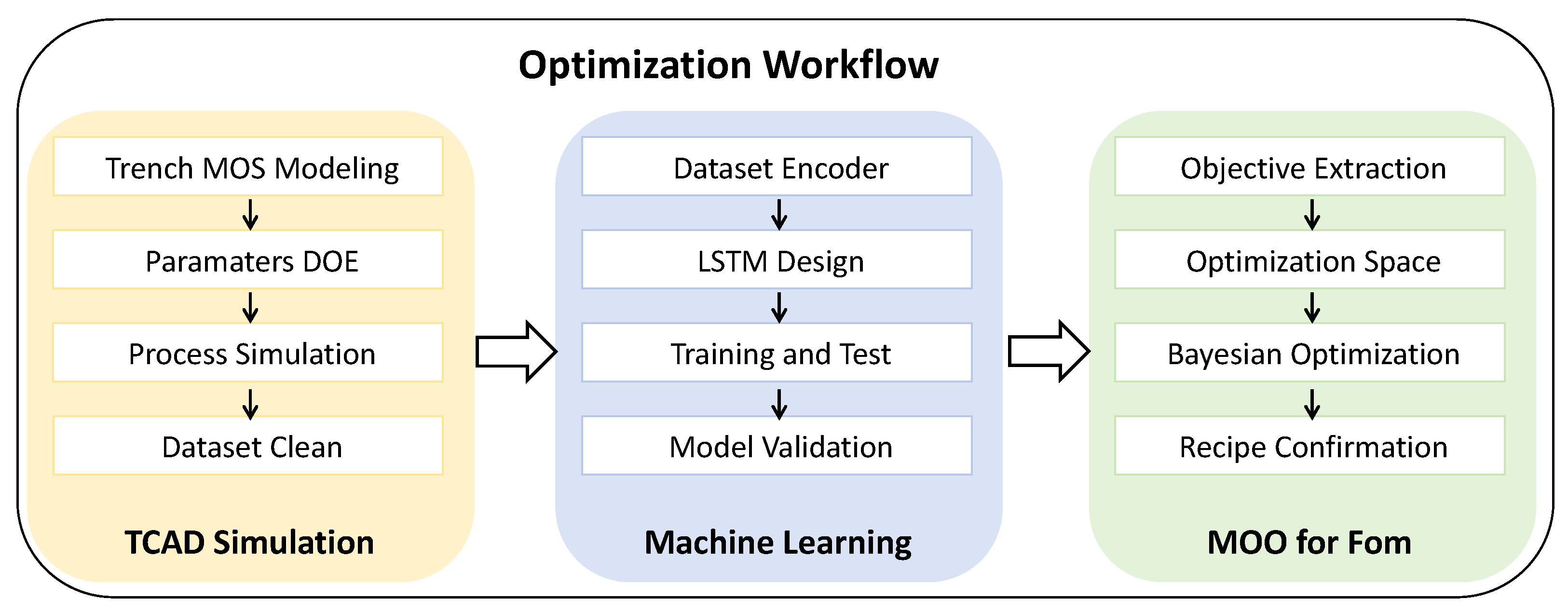
2. Process Simulation
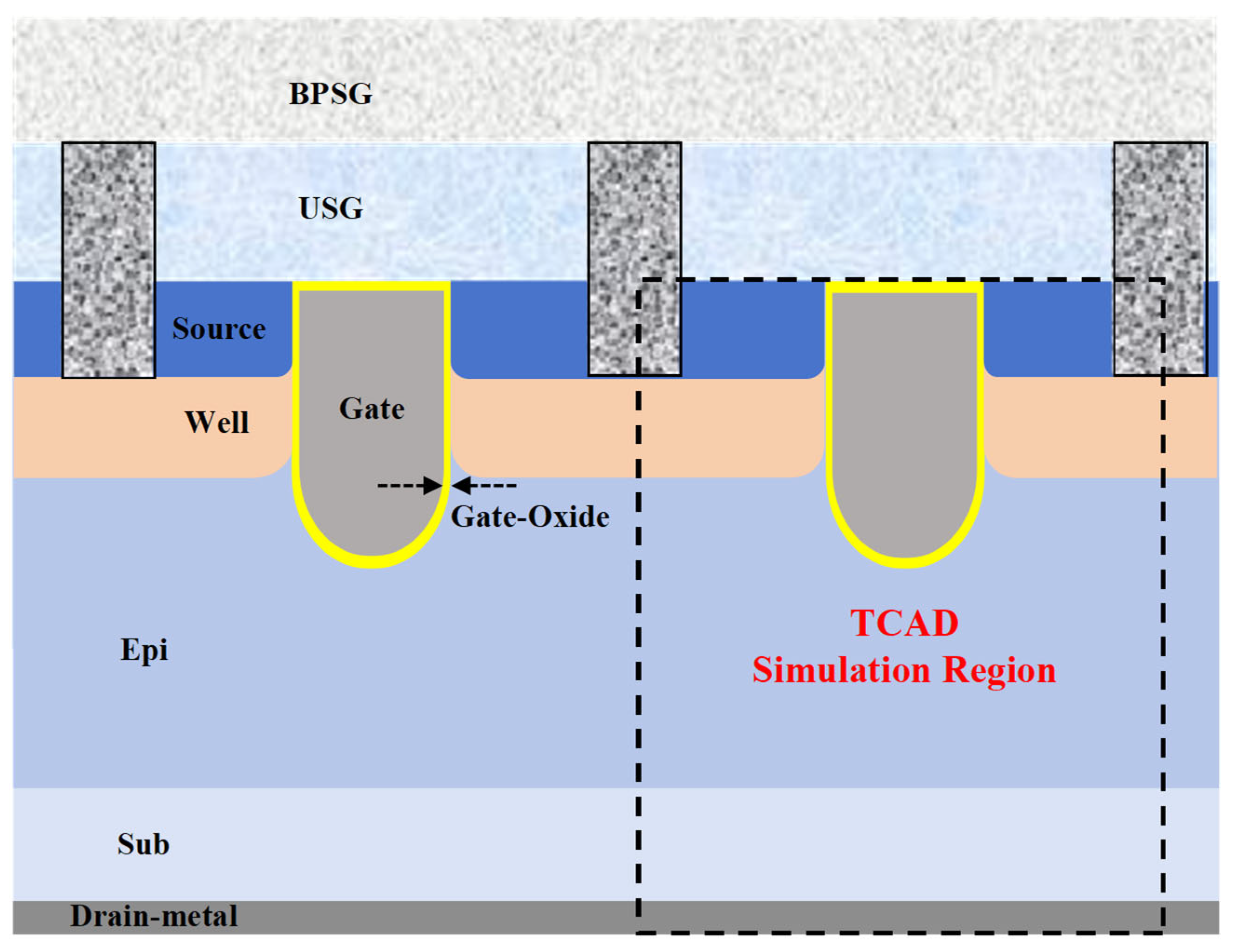
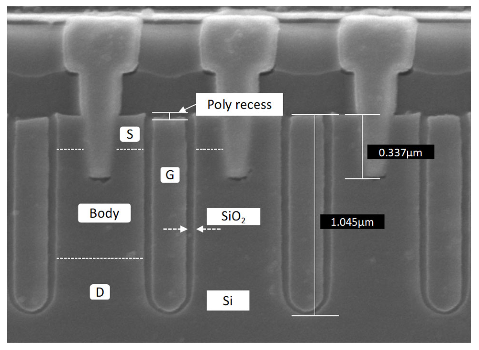
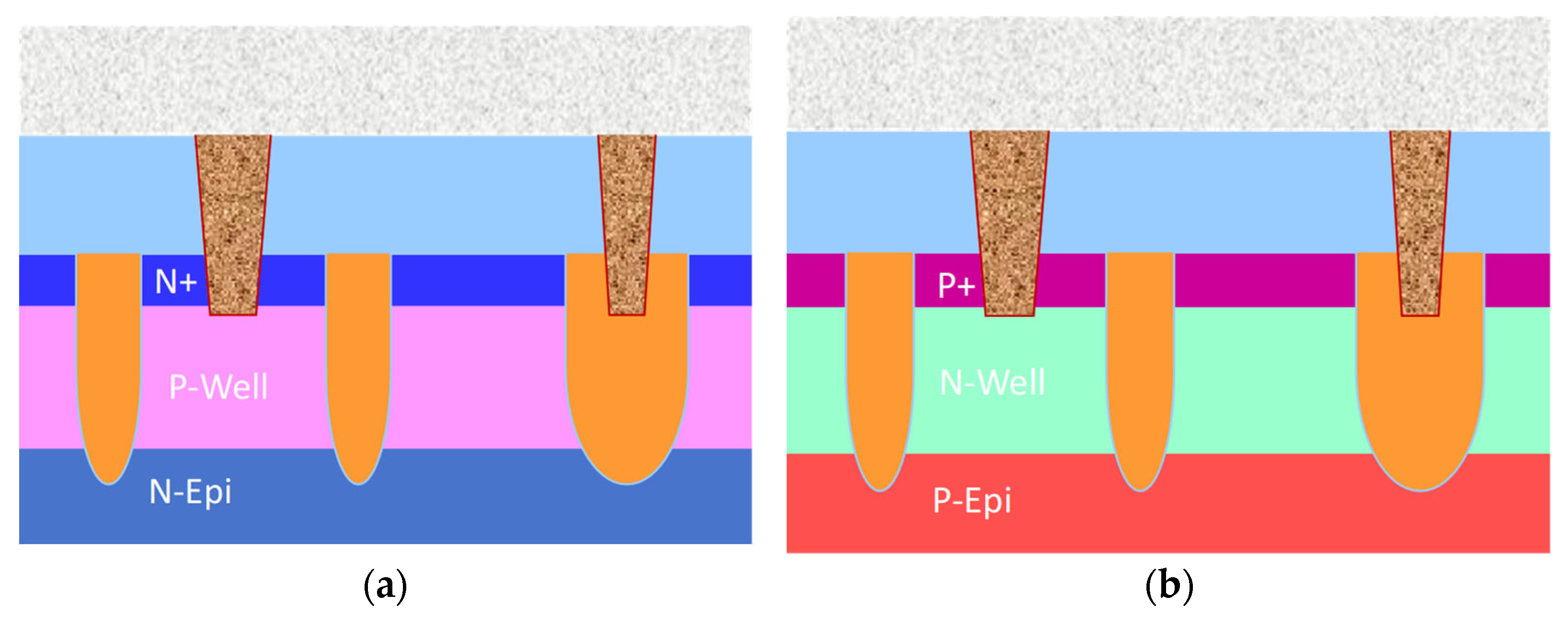
2.1. Trench MOSFET

The trench-gate metal–oxide–semiconductor field-effect transistor (TG-MOSFET) has emerged as a critical component in high-frequency, low-voltage power electronics, particularly for applications such as DC–DC converters. However, conventional TG-MOSFETs are often limited by high reverse recovery charge and switching losses associated with their intrinsic body diode. To address these challenges, a novel trench-gate NMOS device integrated with a Schottky barrier diode (SBD), termed the SBD-TG-NMOS, is proposed. This architecture combines the advantages of trench-gate MOSFETs and Schottky diodes, achieving enhanced electrical performance while retaining robust breakdown characteristics [6,8,29].
The SBD-TG-NMOS features a vertical trench-gate configuration, as depicted in Figure 1. Reduced conduction losses: The integrated SBD provides a low-resistance path during forward conduction, bypassing the MOSFET’s body diode. A key innovation lies in the replacement of the conventional ohmic source contact with a Schottky barrier interface, enabling the integration of a built-in SBD parallel to the MOSFET’s body diode. The trench gate is embedded within a lightly doped epitaxial layer, with a p-well/n-well region defining the channel. The Schottky contact is strategically positioned adjacent to the trench gate, facilitating direct interaction with the drift region during operation. This design ensures efficient current conduction through the SBD during reverse recovery, minimizing parasitic effects.
As can be seen from Figure 2, the cross-sectional scanning electron microscope (SEM) image reveals the structural details of a trench MOSFET. Figure 2 illustrates the structural features of the device, with critical dimensions marked for characterization including the gate oxide layer and trench depth. The etch depths at two strategic locations of the trench MOS structure were measured as 1.045 μm and 0.337 μm, respectively.

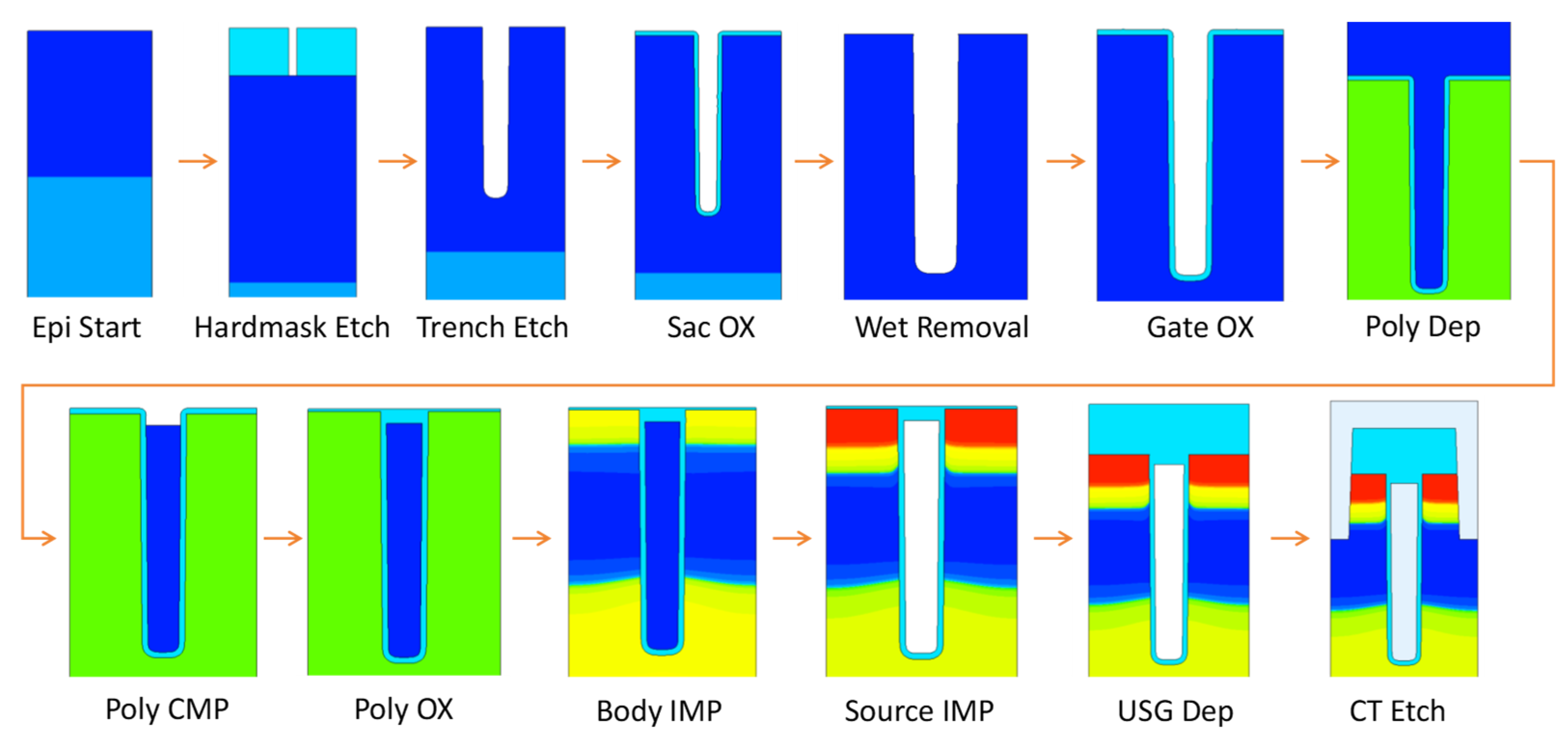
2.2. Device Process Flow

Figure 3 presents a cross-sectional schematic of the TCAD-validated trench MOSFET fabrication process. The manufacturing sequence proceeds as follows: (1) A high-quality semiconductor layer is epitaxially grown on the substrate (Epi Start). (2) Trench regions are defined through hard mask etching (Hardmask Etch), followed by deep trench etching to form vertical structures (Trench Etch). (3) A gate dielectric layer is thermally grown within the trenches (Gate Oxidation). (4) Polysilicon is deposited as gate electrode material (Poly Deposition) and planarized via chemical mechanical polishing (Poly CMP). (5) Sacrificial oxidation (Sac Oxidation) is performed to optimize interface properties. (6) Body region doping is achieved through ion-implantation and annealing processes (Body Implantation/Anneal), followed by source region optimization using analogous techniques (Source Implantation/Anneal). (7) Interlayer dielectric formation is completed with undoped silicate glass deposition (USG Deposition). (8) Metal interconnects are patterned through contact etching (Contact Etch). This process flow integrates advanced etching precision, doping control, and interface optimization techniques, ensuring superior gate controllability and device reliability as validated by TCAD simulations.
Fifteen critical process parameters were systematically identified from the manufacturing sequence, encompassing etch rates and gas flow parameters in patterning steps, temperature–time profiles during oxidation, dose–energy combinations in ion implantation, and thermal budgets in annealing protocols. These variables were selected as the focus of investigation. A full-factorial design of experiments (DOE) framework was implemented to account for all parameter interactions, followed by the generation of statistically representative sample sets for TCAD simulations. This systematic methodology enables comprehensive process–response mapping while maintaining computational efficiency in predictive modeling.
The TCAD process simulation model was calibrated against experimental process conditions and electrical characteristics, achieving strong agreement between simulation and measurement (deviation < 3%).
Figure 4 presents schematic diagrams of two distinct trench MOSFET device architectures. Three TCAD-based trench MOSFET variants (N20 V, N30 V, and P20 V) were constructed for simulation and validation, with identical critical dimensions maintained across all configurations. Key electrical parameters, including breakdown voltage (BV) and resistance (Ron), were found to be predominantly governed by ion-implantation and annealing processes. This correlation enables process recipe modifications during manufacturing to be precisely mirrored in TCAD simulations. The dimensional uniformity allows systematic acquisition of experimental and production data, significantly enhancing model verification accuracy through controlled variable isolation.

3. Methodology

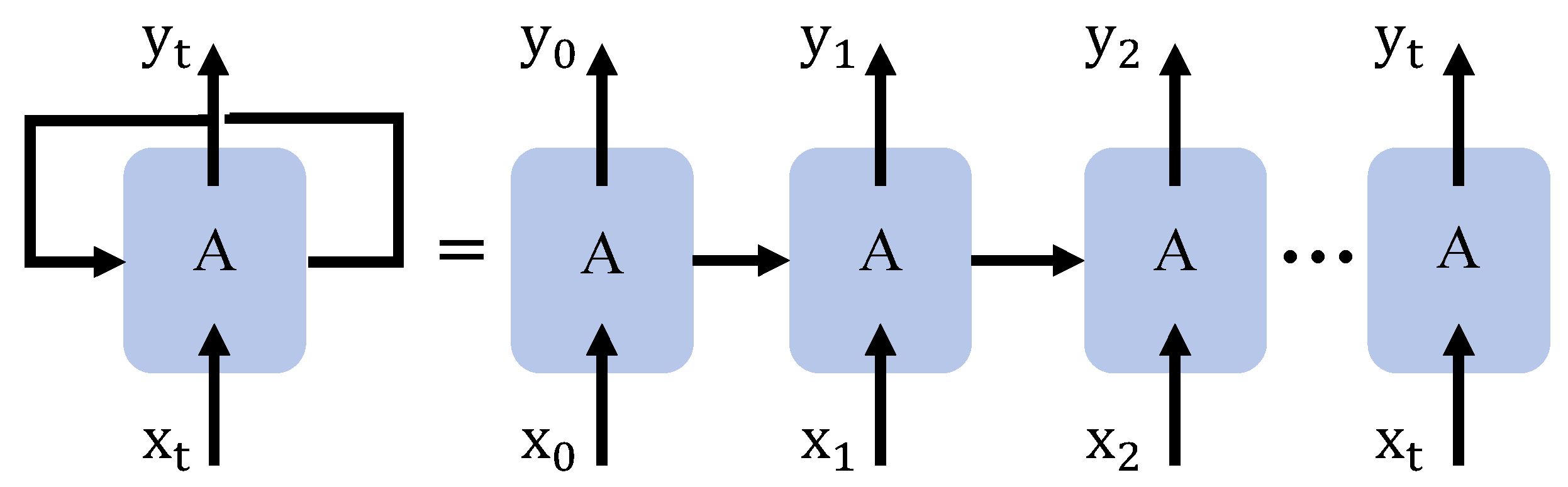
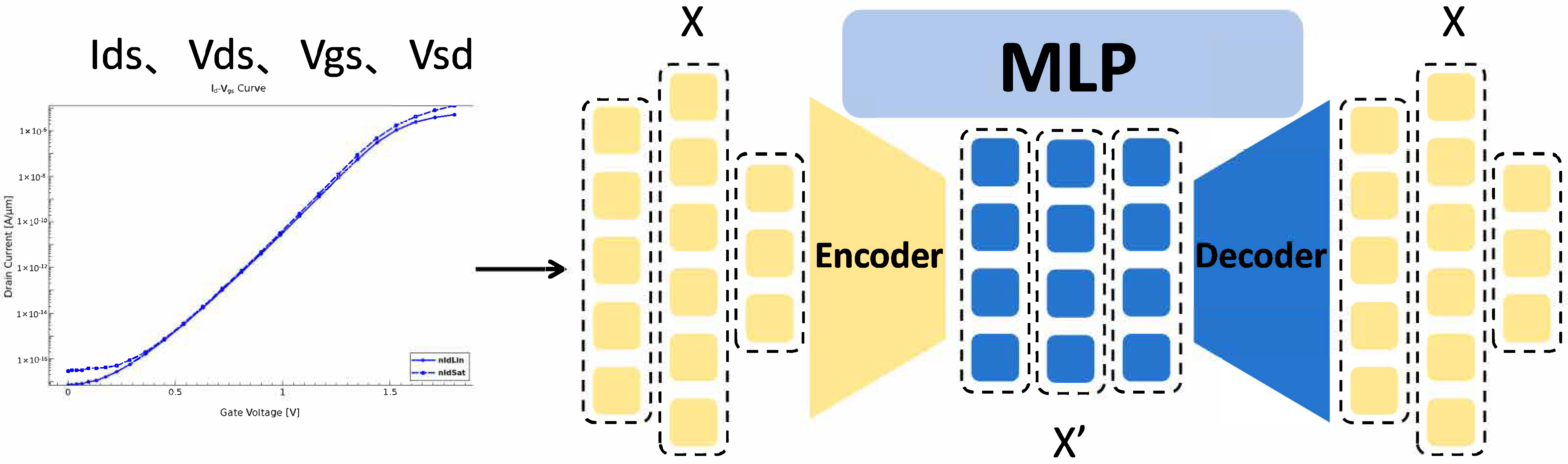
3.1. Machine Learning Methodology

Recurrent neural networks (RNNs) represent a class of artificial neural networks specifically designed to process sequential data by leveraging temporal dependencies. Unlike feedforward networks, RNNs incorporate cyclic connections that enable the retention of historical information through hidden states. This architecture allows the network to map input sequences { x 1 , x 2 , , x T } to output sequences { y 1 , y 2 , , y T } , making them inherently suitable for tasks such as time-series prediction, natural language processing, and dynamic system modeling [19].
Mathematically, the hidden state h t at time step t is updated recursively as follows:
h t = σ ( W x h T · x t + W h h T · h t 1 + b h )
where W x h and W h h are weight matrices for input and recurrent connections, b h is a bias term, and σ(⋅) denotes an activation function (e.g., tanh or ReLU). The output y t is derived from the following hidden state:
y t = W h y T · h t + b y
While RNNs excel at capturing short-term dependencies, their performance degrades for sequences with long-range temporal correlations due to the vanishing/exploding gradient problem. During backpropagation through time (BPTT), gradients used to update network weights diminish or grow exponentially as they propagate across multiple time steps. This instability limits the network’s ability to learn relationships spanning distant time intervals. Additionally, the fixed-size hidden state imposes constraints on memory capacity, further restricting modeling fidelity in applications requiring persistent context retention. As shown in Figure 5, the chain structure diagram of RNNs is given.
To address the limitations of conventional RNNs, long short-term memory (LSTM) networks introduce a gated mechanism that explicitly manages information flow through persistent and transient memory states. This architecture, first proposed by Hochreiter and Schmidhuber [30], enables adaptive retention and forgetting of contextual information over extended sequences.
An LSTM unit comprises three critical components, as shown in Figure 6.
1.
Input gate ( i t ) and candidate state ( g t ): Control the integration of new information into C t with the following:
I n p u t   G a t e:       i t = σ ( W x i T · x t + W h i T · h t 1 + b i )
I n p u t   M o d i l a t i o n   G a t e:       g t = t a n h ( W x g T · x t + W h g T · h t 1 + b g )
2.
Forget gate ( f t ) : Regulates the retention of the persistent memory state C t 1 using the following:
F o r g e t   G a t e:       f t = σ ( W x f T · x t + W h f T · h t 1 + b f )
3.
Output gate ( o t ): Modulates the exposure of C t to the transient state h t through the following:
O u t p u t   G a t e:       o t = σ ( W x o T · x t + W h o T · h t 1 + b o )
4.
The persistent memory state C t is updated via a weighted combination of historical and novel inputs, which can be depicted as follows:
C t = f t C t 1 + i t g t
5.
Where denotes element-wise multiplication. The transient state h t , which serves as the network’s output, is computed as follows:
y t = h t = o t t a n h ( C t )
It has the following advantages over RNNs:
  • Gradient stability: The additive nature of C t mitigates gradient dissipation/explosion, enabling stable training over long sequences.
  • Contextual selectivity: Gating mechanisms allow the network to prioritize relevant temporal features while suppressing noise.
  • Black-box modeling: LSTMs eliminate the need for explicit physical equations, making them ideal for modeling complex nonlinear systems like GaN HEMTs.
By decoupling memory retention from iterative updates, LSTMs achieve superior performance in applications requiring both short-term responsiveness and long-term dependency capture, as demonstrated in subsequent sections. Figure 6 shows a basic unit structure diagram of LSTM.

LSTM Technique-Based Process Model

In the TCAD simulation, the electrical parameters of some devices are solved through iterative generation, exhibiting characteristics of non-uniform sampling. Despite the non-uniform sampling characteristics introduced by iterative parameter solving, fundamental similarities persist in the electrical curves. These recurring patterns originate from the unified physical mechanisms (e.g., carrier transport equations) underlying all simulated devices. Using an encoder–decoder effectively addresses this issue while ensuring the consistency of the data input into the model. Multilayer perception (MLP) network architecture is employed as the core of the encoder–decoder, like Figure 7. The encoder–decoder framework acts as a “smart compressor”:
Encoder: Identifies 5–10 fundamental curve templates from raw data (e.g., exponential saturation curves for Ron).
Decoder: Reconstructs full parameter sets using these templates + process condition inputs.
The fabrication of trench MOSFETs involves sequential process steps with inherent temporal interdependencies, where outputs from prior steps (e.g., etch profiles, oxide thickness) directly define inputs for subsequent stages. To address this sequential complexity, an LSTM network is proposed as a TCAD proxy model. Unlike conventional RNNs, LSTM leverages gate-controlled information flow (input, forget, and output gates) to selectively retain long-range dependencies, effectively mitigating gradient vanishing issues common in multi-step process simulations.
A total of 1768 training data are generated via TCAD simulations calibrated with experimental process recipes and electrical measurements. A design of experiments (DOE) systematically samples critical parameters (e.g., trench depth, gate oxide thickness) across their feasible ranges, ensuring coverage of nonlinear interactions. Electrical test data, including transfer characteristics (Id-Vg), output curves (Id-Vd), and breakdown voltages, are collected under varying bias conditions.
The LSTM network adopts a multi-layer structure, like Figure 8, to hierarchically capture process–device relationships. Each LSTM cell ingests time-step inputs comprising recipe parameters (e.g., reactive gas flow, etch angle) and metrology data (e.g., post-etch critical dimensions). The hidden states propagate sequentially across process steps, emulating the cascading nature of fabrication. For instance, in trench etching simulations, inputs include after-develop inspection (ADI) measurements and recipe variables, while outputs predict after-etch inspection (AEI) profiles. For multi-dimensional parameter spaces inherent to complex processes like ion-implantation, a stacked LSTM architecture with three hidden layers (128/256/128 units each) is deployed to enhance nonlinear mapping capabilities.
The LSTM architecture (3 layers with 128/256/128 units) was optimized through iterative hyperparameter tuning to balance accuracy and computational efficiency. Configurations within common ranges (64–512 units, 2–3 layers) were systematically explored, prioritizing lightweight structures while retaining nonlinear mapping capabilities for high-dimensional process parameters. The final design was selected based on empirical validation, and unit reductions in layers minimized redundancy without compromising fidelity. This approach ensured robustness and alignment with industrial scalability requirements.
The proposed LSTM-based framework is fundamentally constrained by the practical realities of semiconductor manufacturing, where only recipe parameters (e.g., gas flow rates, temperature ramps, plasma power) can be actively monitored and adjusted during processing, whilst the final device characteristics are solely accessible through post-fabrication metrology data (e.g., sheet resistance, threshold voltage, leakage current). This data-driven paradigm necessitates a modeling approach that rigorously maps sequential recipe variations to terminal electrical responses without intermediate physical inspections—a constraint intrinsic to high-volume production environments. Crucially, both input vectors (process recipes) and output responses (electrical metrics) are restricted to numerical representations of controlled variables and measured outcomes, respectively, with process optimization objectives formulated as multivariate regression problems against device specification targets.
The model is implemented in TensorFlow using a Nadam optimizer and means squared error (MSE) loss function. Training converges iteratively, with early stopping triggered when validation loss plateaus—typically within 200 epochs. To enhance robustness, dropout layers (rate = 0.2) are inserted between LSTM layers, regularizing the network against overfitting. Figure 9 shows the training loss function curve.
The sequential chained architecture of recurrent networks demonstrates inherent compatibility with semiconductor manufacturing processes. Among numerous architectural variants (RNN, LSTM, GRU, and Bi-RNN), three predominant frameworks were systematically compared using identical N20V device specifications. Architectural configurations were optimized through layer-wise adjustments to maintain equivalent trainable parameters.
As detailed in Table 1, the standard RNN architecture, despite its simplest gating mechanism (no explicit gates) and fastest extraction time (57.67 s), exhibits limited capability in long-term dependency modeling, resulting in the highest average relative error (2.870%). The LSTM architecture exhibited superior modeling accuracy despite requiring 14% longer computational time per epoch compared to GRU counterparts. The GRU variant introduces moderate gating complexity (update and reset gates) with 13 equivalent layers, achieving improved error reduction (1.323%) at the cost of marginally increased computational overhead (68.92 s). Notably, the LSTM attains the highest parameter efficiency (11 equivalent layers) while maintaining robust long-term dependency capture.
This performance advantage led to the selection of LSTM as the surrogate model, with its gated memory mechanism proving particularly effective in capturing nonlinear process–response relationships inherent to ion implantation and thermal annealing dynamics.

3.2. Multi-Objective Optimization

Based on the LSTM-based forward process model established in the previous section, a Bayesian optimization-driven reverse optimization methodology is proposed in this study to enhance the figure of merit (FoM) of trench MOS devices. This systematic approach enables timely calibration of process recipes during actual manufacturing operations. Figure 10 shows the workflow diagram based on Bayesian multi-objective optimization.
Bayesian optimization (BO) is a probabilistic framework designed for the global optimization of expensive black-box functions [31]. It leverages Gaussian process (GP) regression to model the unknown objective function f ( x ) , where x represents the input parameters. A GP prior is defined by a mean function m ( x ) and a covariance kernel K ( x , x ) , capturing the spatial correlation between parameter configurations. For robustness in modeling non-smooth or heteroscedastic functions, the Matern 5/2 kernel is often preferred over the squared exponential kernel due to its adaptability to varying smoothness assumptions.
The acquisition function, such as expected improvement (EI), guides the iterative selection of subsequent evaluation points by balancing exploration and exploitation. EI quantifies the potential gain over the current best observation f ( x + ) through the following:
a E I x = E [ m a x ( f x + f x , 0 ) ]
which is analytically tractable under the GP posterior. To account for hyperparameter uncertainty, a fully Bayesian treatment integrates over kernel parameters via Markov chain Monte Carlo (MCMC) sampling, ensuring robustness against model misspecification.
In power device optimization, conflicting objectives—such as maximizing breakdown voltage (BV) while minimizing specific on-resistance (Ron)—necessitate a Pareto-optimal framework. The adaptive weighted sum (AWS) method transforms multi-objective problems into scalarized formulations by dynamically adjusting weights to uniformly sample the Pareto front. For the FoM (as Formula (10)), the utility function is defined as follows:
F o m = B V 2 R o n
U x = λ · B V 2 B V m a x + ( 1 λ ) · R o n , m i n R o n
where λ ∈ [0, 1] governs the trade-off between objectives, and normalization ensures dimensionless comparability. AWS refines weight distributions iteratively, prioritizing regions with sparse Pareto solutions to enhance coverage and resolution.
Inverse optimization bridges the gap between target performance metrics and feasible input parameters. Given a pre-trained LSTM model M that predicts BV and Ron from process variables (e.g., trench depth, doping concentration), the inverse problem seeks parameters x* that minimize the deviation from target FoM*, which can be shown as follows:
x * = arg m i n | | M x F o M * | |
BO accelerates this search by constructing a surrogate model of the inverse response surface, enabling efficient exploration of high-dimensional parameter spaces.

4. Results and Discussion

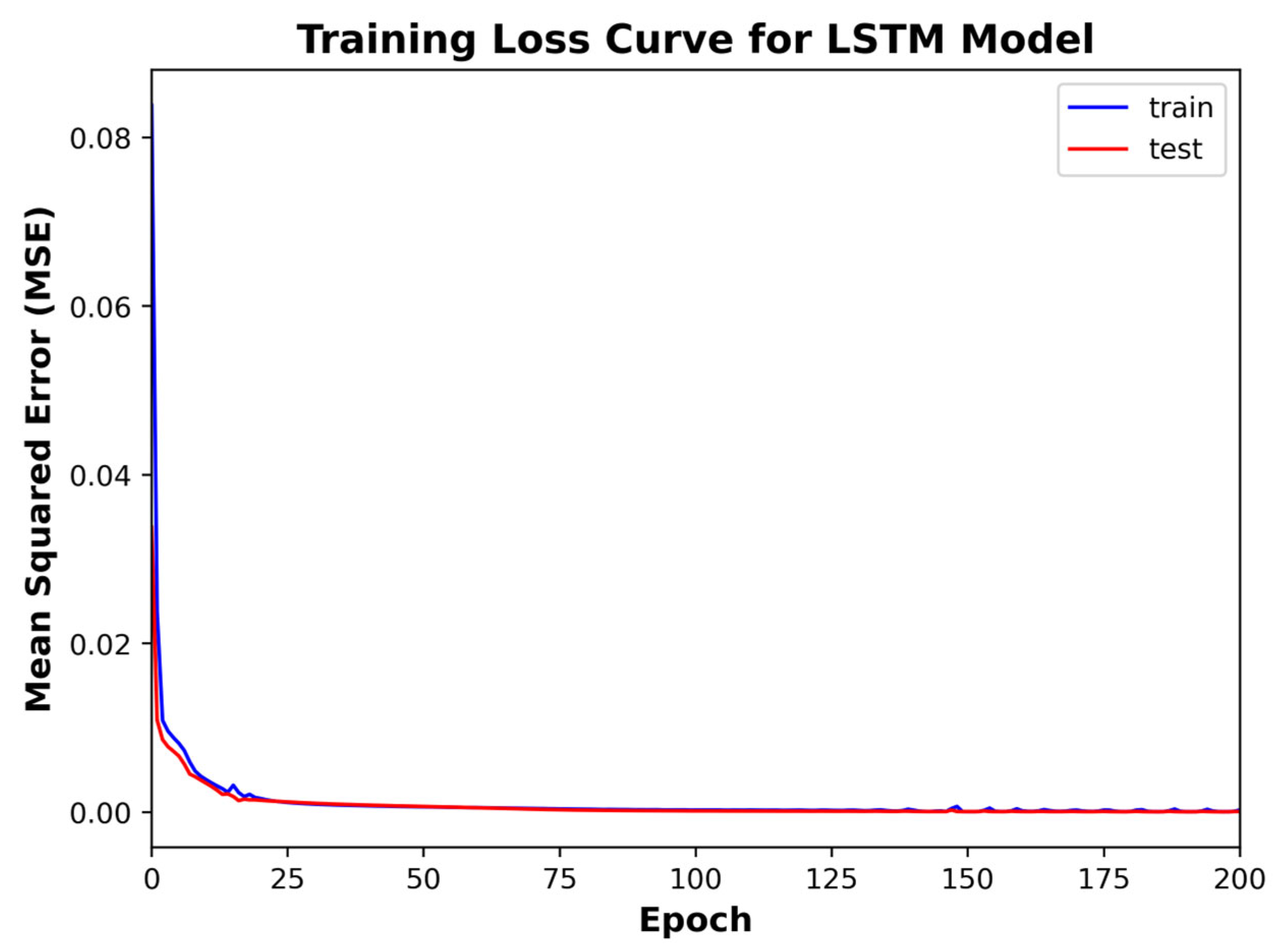
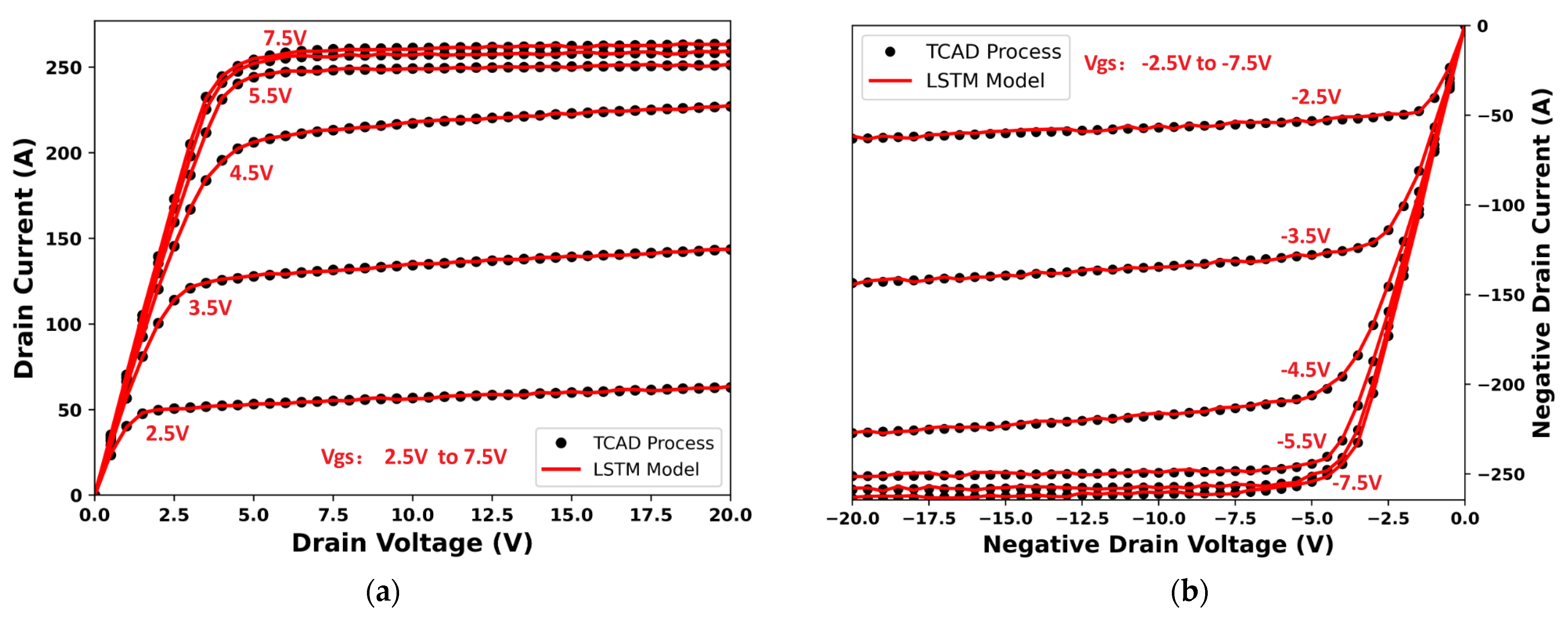
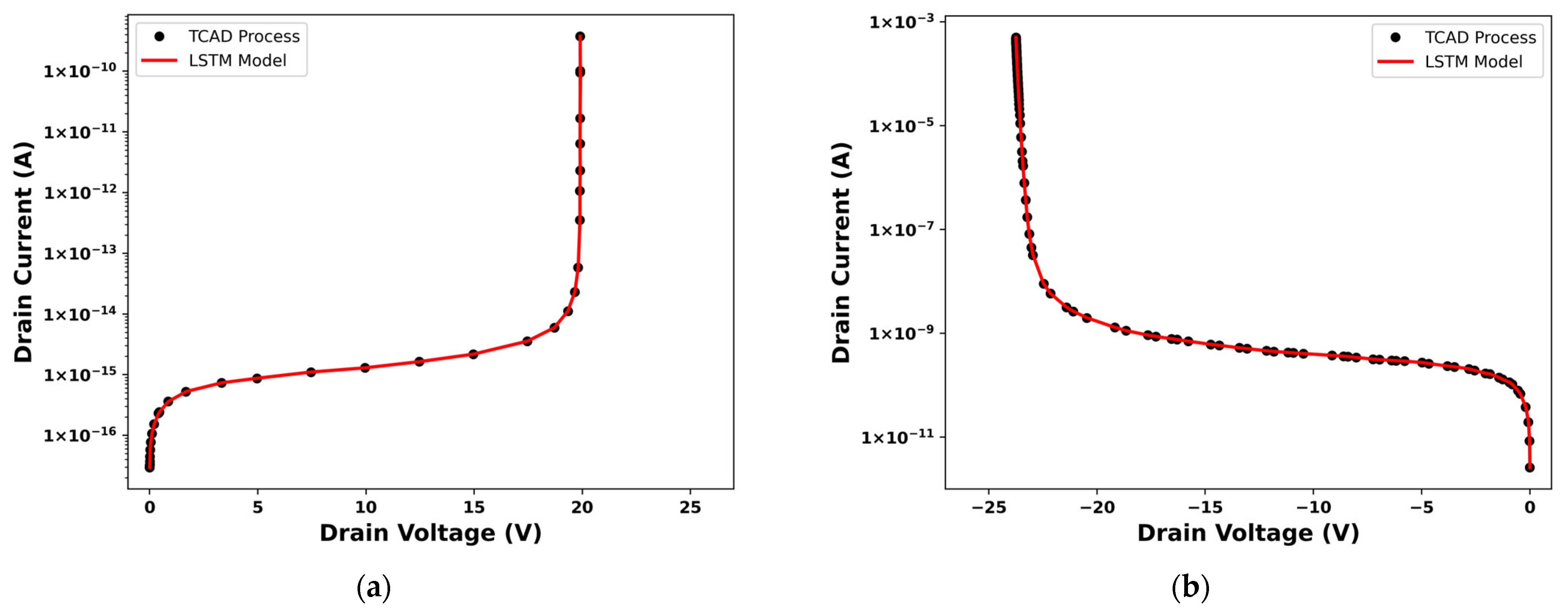
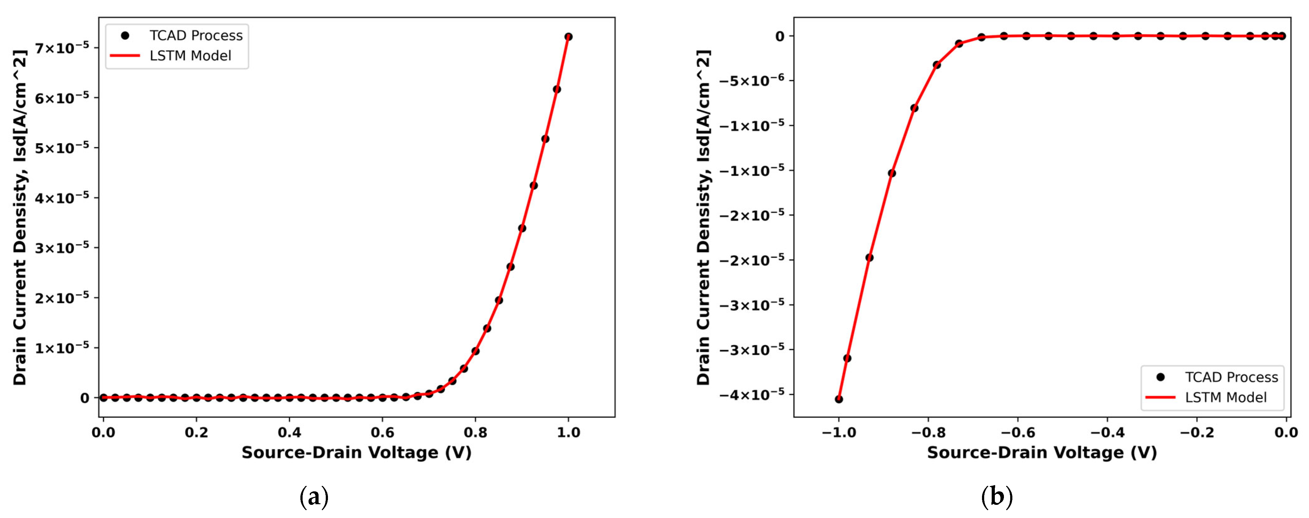
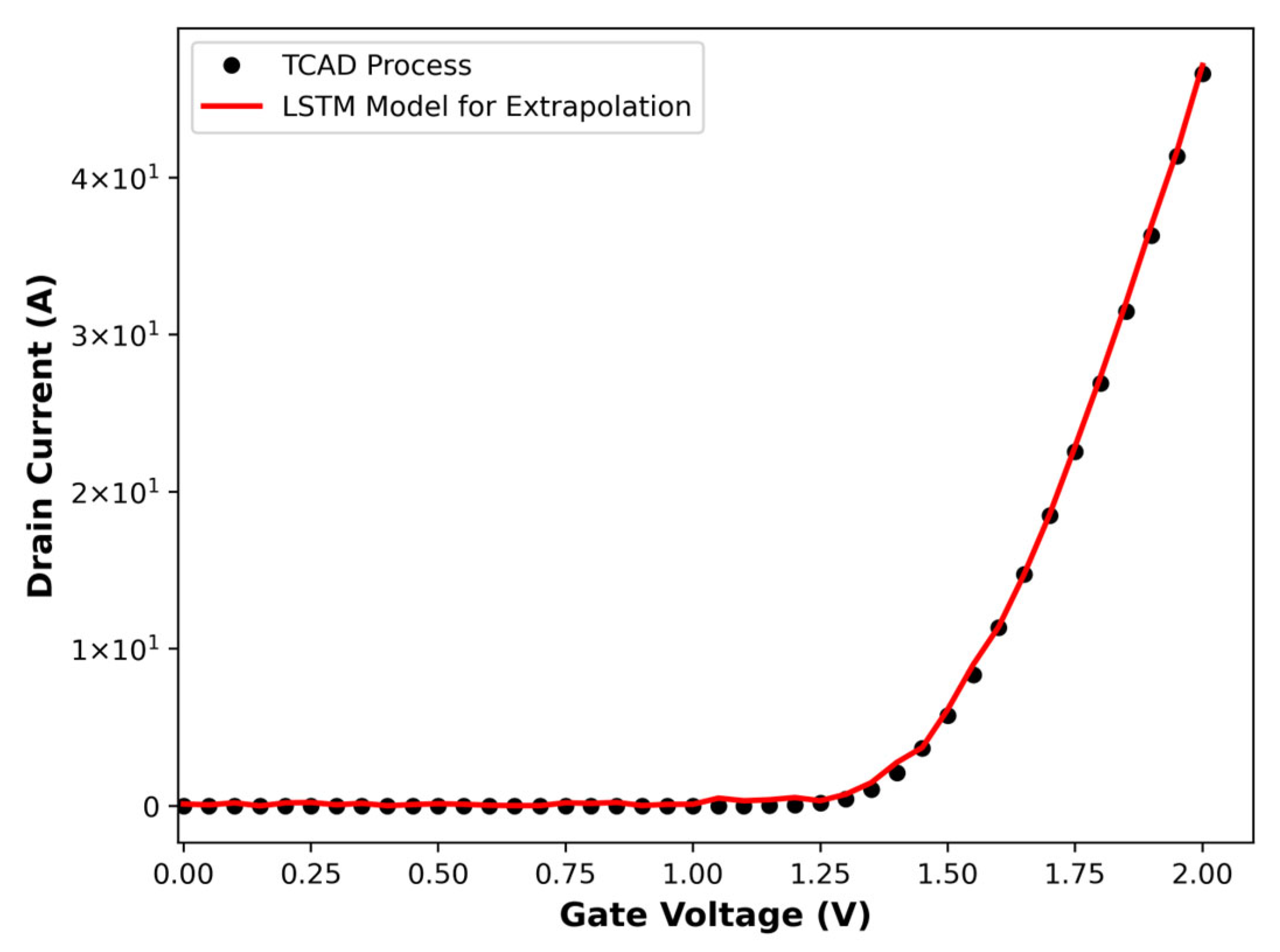
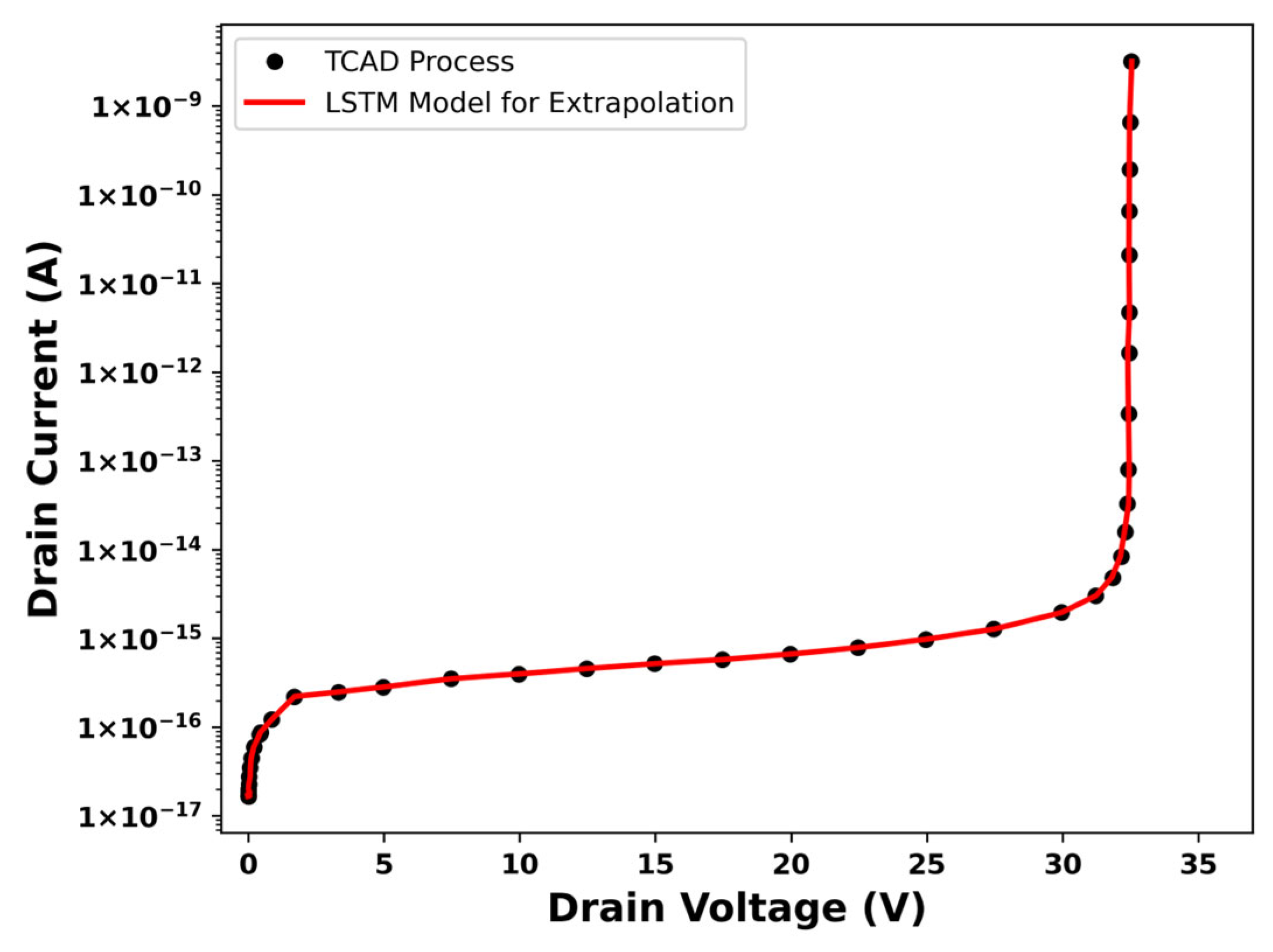
4.1. Model Validation

The predictive capability of the proposed LSTM-based TCAD proxy model was rigorously validated through comprehensive comparisons with conventional TCAD simulations across key electrical parameters of trench MOSFET devices. Figure 11, Figure 12, Figure 13 and Figure 14 illustrate the alignment between LSTM predictions and TCAD-generated data for transfer characteristics, output curves, breakdown voltage, and body diode behavior.
For transfer characteristics (Figure 11), the LSTM model successfully captures the Vth and subthreshold swing (SS) across both NMOS and PMOS configurations, with deviations limited to 0.95% and 1.1%, respectively. This accuracy is attributed to the model’s ability to hierarchically encode nonlinear relationships between process parameters (e.g., gate oxide thickness, doping profiles) and terminal electrical responses. The output characteristics (Figure 12) further demonstrate the model’s fidelity in simulating channel conductance and saturation current, achieving errors below 1.5% even under strong gate voltage nonlinearity.
Breakdown voltage (BV) analysis (Figure 13) reveals that the LSTM framework accurately replicates avalanche breakdown phenomena, with discrepancies of 1.6% (NMOS) and 2.3% (PMOS) compared to TCAD. Body diode characterization (Figure 14) confirms the model’s capacity to predict forward voltage drops (VF) with <1% error, though slight underestimations in PMOS devices suggest opportunities for refining recombination rate calibrations in future iterations.
All the above test cases demonstrate the effectiveness of the LSTM surrogate model in establishing the trench MOS device process flow, ensuring both the efficiency of the model and achieving industrial-level prediction accuracy.
The model’s generalization capability was further validated through extrapolation tests beyond the nominal operating ranges. As shown in Figure 15, transfer characteristics of the N30V device were predicted over an extended gate voltage range (0–2 V) using a model trained exclusively on N20 V device data. The LSTM framework maintains predictive consistency, with an 8.5% deviation in Vth. This capability stems from the LSTM’s gated memory architecture, which selectively retains long-term dependencies in process–device relationships, thereby mitigating error accumulation in multi-step simulations.
Similarly, breakdown voltage extrapolation (Figure 16) demonstrates robust performance under high-field conditions (0–40 V). The model achieves a 6.2% deviation in critical BV parameters, validating its ability to capture nonlinear leakage current dynamics without explicit physical formulations. Such extrapolation accuracy is critical for industrial applications as process variations often necessitate predictions beyond experimentally validated ranges.

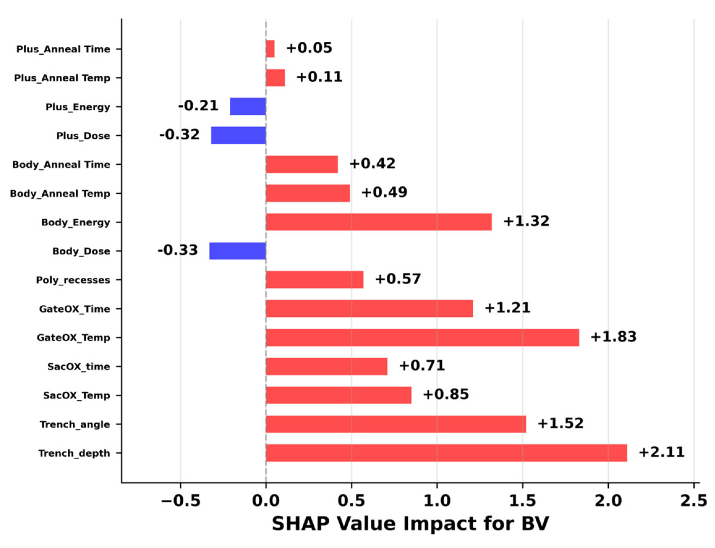
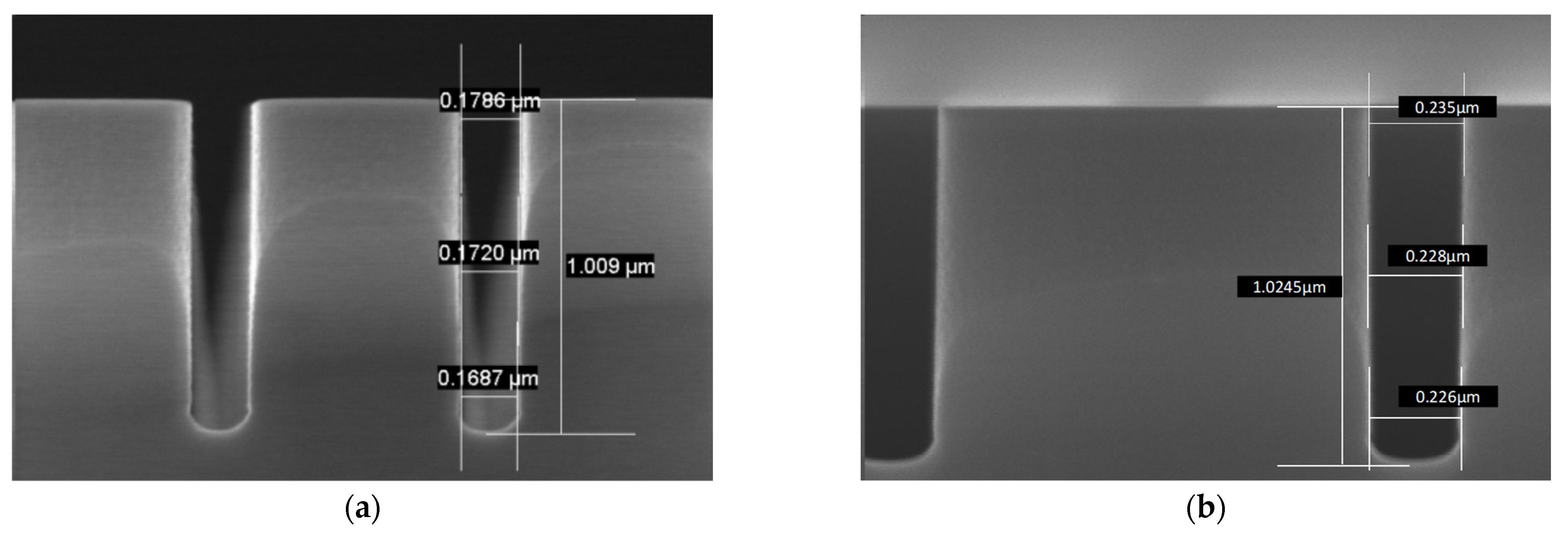
4.2. Inverse Optimization

The inverse optimization capability of the proposed framework was rigorously validated through Bayesian optimization (BO), demonstrating superior performance in navigating high-dimensional process parameter spaces while avoiding local optima. As illustrated in Figure 17, the inverse optimization verification was performed on a single N20V device. To improve the accuracy of inverse optimization and modeling precision, the data for the established forward LSTM fitting model exclusively included all process parameters of N20 V devices, with constant values from fixed process variables removed. The retained 15 key parameters were used to optimize and refine the model. The reduced number of modeling parameters alleviates the search difficulty of Bayesian inverse optimization to some extent. As shown in Figure 17, the definitions of the 15 corresponding process parameters are clearly labeled. The BO-driven parameter predictions exhibit a maximum deviation of 8.3% from actual process recipes across critical variables such as ion-implantation dose, trench etch angle, and gate oxidation time. This precision is attributed to BO’s Gaussian process (GP) regression framework, which probabilistically models the nonlinear relationships between process parameters and device performance metrics (e.g., BV, Ron), enabling efficient exploration of the design space.
To enhance the interpretability of the LSTM model, SHAP analysis was performed to quantify the impact of individual process parameters on the breakdown voltage (BV). As illustrated in the SHAP value summary (as shown in Figure 18), parameters such as trench depth (+2.11), trench angle (+1.52), and gate OX temp (+1.83) exhibited the strongest positive correlations with BV. Conversely, plus dose (−0.32), plus energy (−0.21), and body dose (−0.33) showed minor negative influences, likely due to their indirect effects on carrier mobility and junction leakage.
Notably, trench depth dominated the BV response, aligning with TCAD-simulated electric field distributions where deeper trenches reduced peak field crowding. The hierarchical dependencies revealed by SHAP values further validated the LSTM’s alignment with physical principles. This analysis bridges the “black-box” nature of LSTM with actionable process insights, enabling targeted optimization of critical parameters.
The ion-implantation process recipe parameters obtained through Bayesian backward optimization were used in combination to re-simulate this step in TCAD. As shown in Figure 19, the implanted ions gradually penetrate deeper into the substrate with the increase in annealing time. Furthermore, after annealing, the resulting source maintains a high level of consistency with the original TCAD simulation results.
After evaluating the cost and difficulty of obtaining data in the actual production process, we selected the SAC OX step to demonstrate the performance of Bayesian backward optimization. The SEM images provide a detailed view of the trench dimension changes. The robustness of the methodology was further validated through SEM metrology (Figure 20). The dimensional variation in trenches produced by the wet etching process compared to standard processing parameters remains within acceptable tolerance limits, demonstrating the industrial viability of this methodology.
The validation results of the LSTM-based proxy model and Bayesian optimization framework collectively demonstrate a synergistic approach to trench MOSFET process–device co-optimization. The LSTM model’s high-fidelity predictions provide a computationally efficient surrogate for TCAD simulations, enabling rapid exploration of high-dimensional parameter spaces. This accuracy is critical for BO-driven inverse optimization, where the probabilistic Gaussian process regression leverages the LSTM’s outputs to navigate trade-offs between conflicting objectives with minimal experimental iterations.

5. Conclusions

This study establishes a robust LSTM-Bayesian optimization framework for trench MOSFET process–device co-optimization. The LSTM-based TCAD proxy model achieves industrial-level accuracy, predicting key electrical parameters (e.g., breakdown voltage, threshold voltage) with deviations below 3.5% compared to conventional simulations. Its hierarchical architecture effectively captures nonlinear process–device relationships, outperforming RNN and GRU counterparts by reducing average relative errors by 1.78%. Extrapolation tests validate its generalization capability, with deviations of 8.5% (Vth) and 6.2% (BV) under extended operating ranges highlighting its adaptability to process variations.
Bayesian optimization enables efficient inverse design, identifying optimal process recipes with a maximum 8.3% deviation from actual parameters while balancing conflicting objectives via Pareto optimal trade-offs. Experimental validation through SEM metrology confirms dimensional tolerances within industrial specifications, underscoring practical viability. Future work should refine PMOS recombination rate calibrations and explore hybrid architectures to mitigate computational overhead. This framework bridges TCAD simulations and manufacturing, offering a scalable, data-driven paradigm for next-generation power electronics development.

Author Contributions

Conceptualization, M.G., J.G. and Y.S.; methodology, M.G. and D.N.; software, M.G., J.G., Y.S. and D.N.; validation, M.G.; formal analysis, M.G. and Y.S.; investigation, M.G. and Y.S.; resources, M.G., D.G. and D.N.; data curation, M.G. and Y.S.; writing—original draft preparation, M.G. and D.N.; writing—review and editing, M.G. and D.N.; project administration, M.G. and D.N. All authors have read and agreed to the published version of the manuscript.

Funding

This research received no external funding.

Data Availability Statement

The original contributions presented in this study are included in the article. Further inquiries can be directed to the corresponding author.

Conflicts of Interest

Authors Yuting Sun and Dawei Gao were employed by the company Zhejiang ICsprout Semiconductor Co., Ltd. The remaining authors declare that the research was conducted in the absence of any commercial or financial relationships that could be construed as a potential conflict of interest.

Abbreviations

The following abbreviations are used in this manuscript:
RNNRecurrent Neural Network
LSTMLong Short-Term Memory
GRUGated Recurrent Unit
MOOMulti-Objective Optimization
TCADTechnology Computer-Aided Design
SBDSchottky barrier diode

References

  1. Williams, R.K.; Darwish, M.N.; Blanchard, R.A.; Siemieniec, R.; Rutter, P.; Kawaguchi, Y. The Trench Power MOSFET: Part I—History, Technology, and Prospects. IEEE Trans. Electron. Devices 2017, 64, 674–691. [Google Scholar] [CrossRef]
  2. Williams, R.K.; Darwish, M.N.; Blanchard, R.A.; Siemieniec, R.; Rutter, P.; Kawaguchi, Y. The Trench Power MOSFET—Part II: Application Specific VDMOS, LDMOS, Packaging, and Reliability. IEEE Trans. Electron. Devices 2017, 64, 692–712. [Google Scholar] [CrossRef]
  3. Chuang, C.S.P.; Chen, K.Y.G.; Hung, Y.R.R.; Kuo, T.C.; Huang, C.C.T. Forward-voltage-tunable schottky-integrated trench MOSFETs. In Proceedings of the 2014 IEEE 26th International Symposium on Power Semiconductor Devices & IC’s (ISPSD), Waikoloa, HI, USA, 15–19 June 2014; pp. 159–162. [Google Scholar]
  4. Dolny; Sapp; Elbanhaway; Wheatley. The influence of body effect and threshold voltage reduction on trench MOSFET body diode characteristics. In Proceedings of the 16th International Symposium on Power Semiconductor Devices and ICs, Kitakyushu, Japan, 24–27 May 2004; pp. 217–220. [Google Scholar]
  5. Prado, E.O.; Bolsi, P.C.; Sartori, H.C.; Pinheiro, J.R. An Overview about Si, Superjunction, SiC and GaN Power MOSFET Technologies in Power Electronics Applications. Energies 2022, 15, 5244. [Google Scholar] [CrossRef]
  6. Mirchandani; Thapar; Boden; Sodhi; Kinzer. A novel n-channel MOSFET featuring an integrated Schottky and no internal p-n junction. In Proceedings of the 16th International Symposium on Power Semiconductor Devices and ICs, Kitakyushu, Japan, 24–27 May 2004; pp. 405–408. [Google Scholar]
  7. Hirao, T.; Hashimoto, T. Low Reverse Recovery Charge 30 V Power MOSFET With Double Epi Structure for DC–DC Converters. IEEE Trans. Electron. Devices 2016, 63, 1154–1160. [Google Scholar] [CrossRef]
  8. Hirao, T.; Hashimoto, T.; Shirai, N.; Arai, H.; Matsuura, N.; Matsuura, H. Low reverse recovery charge 30-V power MOSFETs for DC-DC converters. In Proceedings of the 2013 25th International Symposium on Power Semiconductor Devices & IC’s (ISPSD), Kanazawa, Japan, 26–30 May 2013; pp. 221–224. [Google Scholar]
  9. Xiao, C.; Yang, W.; Liu, Y.; Zhou, X.; Feng, H.; Sin, J.K.O. A Trench-Field-Plate High-Voltage Power MOSFET. IEEE Trans. Electron. Devices 2020, 67, 2482–2488. [Google Scholar] [CrossRef]
  10. Xu, H.; Gan, W.; Cao, L.; Yang, C.; Wu, J.; Zhou, M.; Qu, H.; Zhang, S.; Yin, H.; Wu, Z. A Machine Learning Approach for Optimization of Channel Geometry and Source/Drain Doping Profile of Stacked Nanosheet Transistors. IEEE Trans. Electron. Devices 2022, 69, 3568–3574. [Google Scholar] [CrossRef]
  11. Kim, Y.; Myung, S.; Ryu, J.; Jeong, C.; Kim, D.S. Physics-augmented Neural Compact Model for Emerging Device Technologies. In Proceedings of the 2020 International Conference on Simulation of Semiconductor Processes and Devices (SISPAD), Kobe, Japan, 23 September–6 October 2020; pp. 257–260. [Google Scholar]
  12. Liu, C.C.; Li, Y.; Yang, Y.S.; Chen, C.Y.; Chuang, M.H. Automatic Device Model Parameter Extractions via Hybrid Intelligent Methodology. In Proceedings of the 2020 International Conference on Simulation of Semiconductor Processes and Devices (SISPAD), Kobe, Japan, 23 September–6 October 2020; pp. 355–358. [Google Scholar]
  13. Yang, Q.; Qi, G.; Gan, W.; Wu, Z.; Yin, H.; Chen, T.; Hu, G.; Wan, J.; Yu, S.; Lu, Y. Transistor Compact Model Based on Multigradient Neural Network and Its Application in SPICE Circuit Simulations for Gate-All-Around Si Cold Source FETs. IEEE Trans. Electron. Devices 2021, 68, 4181–4188. [Google Scholar] [CrossRef]
  14. Colinge, J.-P.; Lee, C.-W.; Afzalian, A.; Akhavan, N.D.; Yan, R.; Ferain, I.; Razavi, P.; O’Neill, B.; Blake, A.; White, M.; et al. Nanowire transistors without junctions. Nat. Nanotechnol. 2010, 5, 225–229. [Google Scholar] [CrossRef] [PubMed]
  15. Wu, T.; Guo, J. Multiobjective Design of 2-D-Material-Based Field-Effect Transistors with Machine Learning Methods. IEEE Trans. Electron. Devices 2021, 68, 5476–5482. [Google Scholar] [CrossRef]
  16. Crose, M.; Kwon, J.S.-I.; Tran, A.; Christofides, P.D. Multiscale modeling and run-to-run control of PECVD of thin film solar cells. Renew. Energy 2017, 100, 129–140. [Google Scholar] [CrossRef]
  17. Dhillon, H.; Mehta, K.; Xiao, M.; Wang, B.; Zhang, Y.; Wong, H.Y. TCAD-Augmented Machine Learning with and Without Domain Expertise. IEEE Trans. Electron. Devices 2021, 68, 5498–5503. [Google Scholar] [CrossRef]
  18. Han, S.C.; Choi, J.; Hong, S.M. Acceleration of Semiconductor Device Simulation with Approximate Solutions Predicted by Trained Neural Networks. IEEE Trans. Electron. Devices 2021, 68, 5483–5489. [Google Scholar] [CrossRef]
  19. Xiao, T.; Ni, D. Multiscale Modeling and Recurrent Neural Network Based Optimization of a Plasma Etch Process. Processes 2021, 9, 151. [Google Scholar] [CrossRef]
  20. Myung, S.; Kim, J.; Jeon, Y.; Jang, W.; Huh, I.; Kim, J.; Han, S.; Baek, K.h.; Ryu, J.; Kim, Y.S.; et al. Real-Time TCAD: A new paradigm for TCAD in the artificial intelligence era. In Proceedings of the 2020 International Conference on Simulation of Semiconductor Processes and Devices (SISPAD), Kobe, Japan, 23 September–6 October 2020; pp. 347–350. [Google Scholar]
  21. Liu, P.; Wu, Q.; Ren, X.; Wang, Y.; Ni, D. A deep-learning-based surrogate modeling method with application to plasma processing. Chem. Eng. Res. Des. 2024, 211, 299–317. [Google Scholar] [CrossRef]
  22. Graves, A.; Mohamed, A.r.; Hinton, G. Speech recognition with deep recurrent neural networks. In Proceedings of the 2013 IEEE International Conference on Acoustics, Speech and Signal Processing, Vancouver, BC, Canada, 26–31 May 2013; pp. 6645–6649. [Google Scholar]
  23. Geng, M.; Crupi, G.; Cai, J. Accurate and Effective Nonlinear Behavioral Modeling of a 10-W GaN HEMT Based on LSTM Neural Networks. IEEE Access 2023, 11, 27267–27279. [Google Scholar] [CrossRef]
  24. Guo, J.; Geng, M.; Ren, K.; Ni, D.; Gao, D. Optimizing Plasma Etching: Integrating Precise Three-Dimensional Etching Simulation and Machine Learning for Multi-Objective Optimization. IEEE Access 2024, 12, 127065–127073. [Google Scholar] [CrossRef]
  25. Geng, M.; Zhu, Z.; Cai, J. Small-Signal Behavioral Model for GaN HEMTs based on Long-Short Term Memory Networks. In Proceedings of the 2021 IEEE MTT-S International Wireless Symposium (IWS), Nanjing, China, 23–26 May 2021; pp. 1–3. [Google Scholar]
  26. Olajire, T.O. Accelerating Manufacturing Decisions Using Bayesian Optimization: An Optimization and Prediction Perspective. Master’s Thesis, West Virginia University, Morgantown, WV, USA, 2023. [Google Scholar]
  27. Shrivastava, A.; Kalaswad, M.; Custer, J.O.; Adams, D.P.; Najm, H.N. Bayesian optimization for stable properties amid processing fluctuations in sputter deposition. J. Vac. Sci. Technol. A 2024, 42, 033408. [Google Scholar] [CrossRef]
  28. Zhang, H.P.; Sun, C.L.L.; Jiang, C.L.F.; Xu, L.Y.; Lin, M. Process simulation of trench gate and plate and trench drain SOI nLDMOS with TCAD tools. In Proceedings of the 2008 IEEE International Conference on Semiconductor Electronics, Johor Bahru, Malaysia, 25–27 November 2008; pp. 92–95. [Google Scholar]
  29. Ono, S.; Yamaguchi, Y.; Matsuda, N.; Takano, A.; Akiyama, M.; Kawaguchi, Y.; Nakagawa, A. High density MOSBD (UMOS with built-in Trench Schottky Barrier Diode) for Synchronous Buck Converters. In Proceedings of the 2006 IEEE International Symposium on Power Semiconductor Devices and IC’s, Naples, Italy, 4–8 June 2006; pp. 1–4. [Google Scholar]
  30. Hochreiter, S.; Schmidhuber, J. Long Short-Term Memory. Neural Comput. 1997, 9, 1735–1780. [Google Scholar] [CrossRef] [PubMed]
  31. Graczyk, K.; Witkowski, K. Bayesian Reasoning for Physics Informed Neural Networks. arXiv 2023, arXiv:2308.13222. [Google Scholar]
Figure 1. Cross-sectional structures of trench MOSFETs in this work. Black dashed line area is simulation with TCAD.
Processes 13 01544 g001
Figure 2. Trench MOSFET as observed in a scanning electron microscope (SEM) image. The image was acquired at 60 kX magnification, with a scale bar of 500 nm. Here, the trench depth was measured as 1.045 μm, with the contact depth determined to be 0.337 μm.
Processes 13 01544 g002
Figure 3. The process flow diagram for the manufacturing of the SBD-TG-MOS, based on TCAD simulation. Here, the abbreviation “Sac” denotes sacrificial; “OX” denotes oxidation; “Dep” denotes deposition; “CMP” denotes chemical mechanical planarization; “IMP” denotes implantation; and “CT” denotes contact.
Processes 13 01544 g003
Figure 4. Schematic diagram of two different types of trench MOSFET structures. (a) an N-channel structure is implemented with an N-type substrate and source electrode, complemented by a P-type well region; (b) a P-channel structure is implemented with a P-type substrate and source electrode, complemented by an N-type well region.
Processes 13 01544 g004
Figure 5. Basic structure concept deployment diagram of RNNs.
Processes 13 01544 g005
Figure 6. The internal architecture of a long short-term memory (LSTM) neural network cell is structured around four gated computational branches. Nonlinear transformations are governed by sigmoidal (σ) and hyperbolic tangent (tanh) activation functions, with denoting element-wise summation and indicating Hadamard product operations.
Processes 13 01544 g006
Figure 7. The topology of encoding and decoding processes of electrical parameters in this study. MLP architecture is adopted as the encoder–decoder. Here, X represents the non-uniform sampled data of the encoder, and X’ denotes the feature points with the same number of points after compression.
Processes 13 01544 g007
Figure 8. The schematic diagram of the LSTM-based proxy model describes the strategy for input and output. Input section: It is sequentially organized according to the process steps and integrated with the LSTM architecture. Output section: Multiple electrical parameters of the device are processed through an encoder.
Processes 13 01544 g008
Figure 9. The training loss function curve of the proposed LSTM model.
Processes 13 01544 g009
Figure 10. Schematic diagram of the overall workflow of the figure of merit (FoM) optimization of trench MOS.
Processes 13 01544 g010
Figure 11. Transfer characteristics of the trench MOS in the LSTM model compared to the TCAD process simulation. The drain work function is set as 10 V to fix the drain current 250 μA; (a) performance comparison of N-type trench MOS devices; (b) performance comparison of P-type trench MOS devices.
Processes 13 01544 g011
Figure 12. Output characteristics of the trench MOS in the F-RNN model compared to the TCAD process simulation. The gate voltage is evenly set in the range from 2.5 V to 7.5 V; (a) performance comparison of N-type trench MOS devices; (b) performance comparison of P-type trench MOS devices.
Processes 13 01544 g012
Figure 13. Breakdown voltage characteristics of the trench MOS in the F-RNN model compared to the TCAD process simulation. The breakdown voltage (BV) was determined with the drain current fixed at 250 μA; (a) performance comparison of N-type trench MOS devices; (b) performance comparison of P-type trench MOS devices.
Processes 13 01544 g013
Figure 14. Body diode characteristics of the trench MOS in the F-RNN model compared to the TCAD process simulation. This study characterizes the forward voltage drop of the body diode. (a) Performance comparison of N-type trench MOS devices; (b) performance comparison of P-type trench MOS devices.
Processes 13 01544 g014
Figure 15. The extrapolation simulation results of the trench MOSFET transfer characteristics with the N30 V device, validated through the LSTM model over an extended gate voltage range (0–2 V), demonstrate predictive consistency with less than 3.5% deviation in threshold voltage parameters. The model is extracted from the N20 V device.
Processes 13 01544 g015
Figure 16. The extrapolation simulation results of the trench MOSFET breakdown voltage (BV) with the N30 V device, validated through the LSTM model over an extended drain-to-source voltage range (0–40 V), demonstrate predictive consistency with less than 2.2% deviation in critical breakdown parameters. The model is extracted from the N20 V device.
Processes 13 01544 g016
Figure 17. Comparison between the actual process parameter values and the optimization values from the BO.
Processes 13 01544 g017
Figure 18. SHAP value analysis of process parameters impacting breakdown voltage (BV).
Processes 13 01544 g018
Figure 19. The cross-sectional view of ion implantation in TCAD simulation, where the recipe is derived from the parameters based on Bayesian backward optimization. Here, from t1 to t6 is represented as six annealing times from start to end.
Processes 13 01544 g019
Figure 20. SEM images of the device before and after the SAC Oxide layer process, and the recipe parameters of the SAC OX process derived from Bayesian backward optimization. (a) SEM image after the trench ETCH process; (b) SEM image after the wet removal process.
Processes 13 01544 g020
Table 1. Performances comparison of different models.
ModelTotal Layers
(Equivalent Parameters)
Gating ComplexityParameters per LayerLong-Term
Dependency Capture
Extraction Time (s)Average
Relative Error (%)
RNN16NoneLowestWeak57.672.870
GRU13Moderate (2 gates)LowerModerate68.921.323
LSTM11High (3 gates)HigherStrong78.261.092
Disclaimer/Publisher’s Note: The statements, opinions and data contained in all publications are solely those of the individual author(s) and contributor(s) and not of MDPI and/or the editor(s). MDPI and/or the editor(s) disclaim responsibility for any injury to people or property resulting from any ideas, methods, instructions or products referred to in the content.

