Abstract
We demonstrated soldering of an electrical component (the metal-oxide semiconductor field effect transistor (MOSFET)) on a printed circuit bord (PCB) via solder paste heated by microwave irradiation. The behavior of the object soldered with solder heated in a microwave magnetic field and electric field were evaluated by using various microwave resonators. In the magnetic field, the solder paste was selectively heated by microwave irradiation. We confirmed that the MOSFET was connected onto the PCB without any damage and that the MOSFET operated normally. However, in an electric field, the solder paste cannot be heated by microwave irradiation because the edges of the PCB were selectively heated. Consequently, the MOSFET could not be connected onto the PCB. The strengths of the electromagnetic fields produced by different microwave resonators were numerically simulated to determine the optimal positions for microwave soldering. Based on the simulation results, microwave heating with separate magnetic and electric fields was carried out and we investigated the heating characteristics of the samples. The appearance and cross sections of the samples were observed by using scanning electron microscopy and energy dispersive X-ray spectroscopy. To estimate any damage by microwave irradiation of the MOSFET, we evaluated the output and transfer characteristics of the MOSFET. We conclude that microwave heating in a magnetic field was superior to heating with an electric field.
1. Introduction
Soldering is the most reliable method for connecting electronic components and is among the technologies that are essential to the production of today’s electronic components. There are two main types of soldering methods: flow soldering and reflow soldering [1,2]. In flow soldering, the printed circuit board (PCB) on which the electronic components are placed is immersed in a bath of melted solder, and the electronic components are connected. Reflow soldering involves printing soldering paste onto a PCB through a metal mask, mounting of electronic components, and then heating the sample with a heating source such as infrared radiation and hot air. Reflow soldering is currently the mainstream connecting method because of its low usage of solder and suitability for surface mounting.
To avoid bonding defects in the reflow soldering process, the electronic components placed on the PCB with soldering paste are preheated, and then the temperature is raised to the melting point of the solder paste for bonding. For lead-free solder, which has become mainstream in recent years, the preheating temperature must be higher than the temperature used to preheat lead solder. Because the temperature of the reflow furnace must be kept high, the consumption of energy associated with reflow soldering has been increasing. Efforts to decrease energy consumption associated with reflow soldering have focused on development of methods to directly heat solder paste with microwaves [3,4,5], high frequency [6], and laser light [7,8] rather than conventional heating methods that use infrared radiation and hot air. In the case of heating with high frequency waves, Li et al. reported that induction heating of solder balls is a local melt process [6]. They used experiments and simulations to discuss the positions of the heated samples, which consisted of solder balls and pads. Nowottnick and Diehm reported the use of soldering microwave heating for three-dimensional PBC assemblies [3]. They reported, in particular, the development of solder materials for the microwave reflow processes, the process itself proceeded within the joint research project “MICROFLOW”.
We are working on heating with electromagnetic radiation in the microwave region and focused especially on microwave heating in a “magnetic field” (herein called magnetic field heating) for a mounting technology [9] and a chemical process [10].
Magnetic field heating is suitable for heating metal because of heat generation due to eddy current loss. In addition, a portion of the strongest magnetic field corresponds to the lowest electric field strength. Arc discharge from the metal is consequently inhibited because no excessive electric potential is applied to the metal.
We previously demonstrated the utility of magnetic field heating for mounting a digital humidity and temperature sensor on a poly(ethylene terephthalate) (PET) film with a Sn-Bi, low-temperature solder paste: the sensor was then mounted without any damage [9]. Although we elucidated the characteristics of magnetic field heating, differences between the effects of heating with a magnetic field and electric field on the mounting of components has not been evaluated in detail.
In this study, we used magnetic field heating of solder to connect a transistor (metal-oxide semiconductor field effect transistor (MOSFET)) onto a PCB via solder paste (Sn96.5-Ag3.0-Cu0.5, SAC305). We then evaluated the condition of the solder joint and its electrical characteristics such as its output and transfer of electrical signals. We discuss, in particular, the differences between the states of samples heated with a magnetic field versus an electric field. We conclude that magnetic field heating was suitable for soldering electrical components.
2. Materials and Methods
2.1. Materials
We obtained SAC305, lead-free solder paste (ECO SOLDER PASTE M705; Senju Metal Industry Co., Ltd., Tokyo, Japan), which has a melting point of 220 °C. The solder paste was used as received without further addition of solvent or flux. We used a transistor and an adapter board, including an N-channel MOSFET heat spreader (2SK4033, Toshiba, Tokyo, Japan) and a semiconductor package to a single in-line package (SIP) patch transfer adapter board (AE-TO-252-SIP, Akizuki Denshi Tsusho Co., Ltd., Tokyo, Japan). The transistor was used as received. The transfer adapter was used after pre-cleaning with acetone.
2.2. Preparation of a Heated Sample and Microwave Irradiation
Solder paste was manually printed onto the adaptor board through a metal mask (thickness, 120 μm). A transistor was manually placed on the printed solder paste.
2.3. Microwave Irradiation
The microwave irradiation system that we used was previously described and is therefore described only briefly here (Figure 1). The system consisted of a microwave generator, a matching box, a cavity, and a thermo camera. The microwave generator (max. power, 400 W; oscillation frequency, 2.4–2.5 GHz; Ryowa Electronics Co., Ltd., Miyagi, Japan) consisted of a controller, an oscillator, an attenuator, a microwave amplifier, an isolator, and an electromagnetic field sensor. The generated microwaves were input to the cavity through a matching box. The matching box was used to tune the impedance between the microwave generator and the cavity. For the microwave irradiation in a magnetic field and an electric field, we used cavities with a TM110 mode (inner diameter φ = 146 mm, L = 100 mm) and TM010 mode (inner diameter φ = 91 mm, L = 100 mm), respectively. A polyimide film (thickness, 125 μm) was used as a stage to set the sample in the cavity.
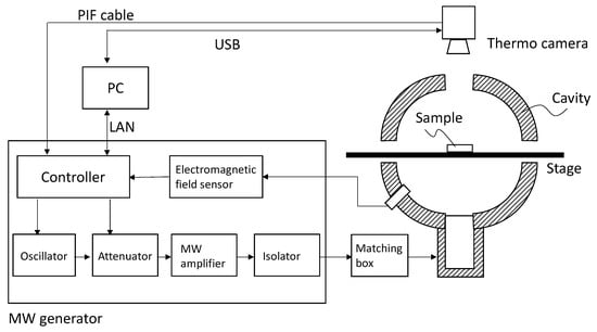
Figure 1.
Schematic diagram of the microwave (MW) heating system. PIF: process interface; USB: universal serial bus; LAN: local area network.
The temperature of the heated sample, which we measured with an infrared camera (PI400i, Optris Co., Berlin, Germany), ranged from 0 to 250 °C. To estimate the temperature of the sample, we first measured the emissivity of each part of the sample by putting the sample in a blackbody furnace (BBZ5-30W1000, Japansensor Corp., Tokyo, Japan), and the emissivity was adjusted so that the temperature of the black body and the sample were the same. The temperature signal was input from the infrared camera to the controller through a process interface cable.
The optical image of the inside of the cavity was recorded with a universal serial bus camera (L-851, Hozan Tool Ind. Co., Ltd., Osaka, Japan) attached with a zoom lens (L-870, Hozan, Osaka, Japan).
2.4. Conventional Reflow
Soldering by a conventional reflow was performed using two electric furnaces (ROP-001P, AS ONE). Temperatures of the furnaces were set at 140 and 260 °C, respectively. The furnaces were preheated for 1 h to stabilize the temperature. A sample was heated for 3 min at 140 °C for flux activation, and then heated for 2 min at 260 °C for melting solder.
2.5. Analysis and Evaluation
After microwave heating, the sample was polished with a polishing machine (ISPP-1000, Ikegami Seiki Co., Ltd., Tokyo, Japan) to facilitate observation of cross-section images with a digital microscope (RH-2000, Hirox Co., Hackensack, NJ, USA) attached to a zoom lens (MXB-2500REZ, Hirox, Tokyo, Japan).
Scanning electron microscopy (SEM) and energy dispersive X-ray spectroscopy (EDS) were performed to confirm the formation of an alloy phase between the solder and copper pad. The observation was performed by using a JSM-7200F (JEOL, Tokyo, Japan) equipped with an EDS detector. The acceleration voltages for the SEM and EDS observation were 15 and 20 kV, respectively.
To measure any damage to the MOSFET by microwave heating, the performance of the transistor was measured with a semiconductor device parameter analyzer (B1500A, Keysight Technologies Corp., Santa Rosa, CA, USA) attached to a probe (SM-1A, Measure Jig, Tokyo, Japan).
A bonding strength of a soldered sample was measured by using a Series 4000 (Nordson Dage, Buckinghamshire, UK). A shear load was applied to the sample at a height of 100 μm above the substrate at a rate of 100 μm/s at room temperature.
2.6. Field Strength of Electromagnetic Field in the Cavity
Numerical simulation of the distribution of electromagnetic radiation was performed with COMSOL Multiphysics software (version 5.6, COMSOL, Inc., Burlington, Burlington Township, NJ, USA) with an RF module. Resonance conditions in the TM110 and TM010 modes were simulated at frequencies of 2.4–2.5 GHz. The dimensions of the cylindrical cavity for the TM110 mode were modeled for diameter 146 mm and length 100 mm. The dimensions of the cylindrical cavity for the TM010 mode were modeled for diameter 91 mm and length 100 mm. The distributions of the magnetic and electric fields were plotted based on the resultant resonance conditions.
3. Theory
Heat Generation in Metal by Microwave Irradiation
Power dissipation by electromagnetic heating with a magnetic field and electric field is briefly described in this section. Equations needed to derive the results can be found in a book such as Foundations of Electroheat [11].
The intensity of an electromagnetic wave is the energy per second crossing a unit area normal to the direction of propagation. It can be described by the Poynting vector S:
where E and H are the magnitudes of the electric field and magnetic field, respectively.
Power dissipation of matter by the electromagnetic wave is calculated by taking the divergence of Equation (1) and substituting Maxwell’s equation:
where σ, ω, μ″, and ε″ are the conductivity of the substance, angular frequency of the radiation, magnetic loss, and dielectric loss, respectively. Equation (2) shows that the power dissipation of the matter by microwave irradiation depends on the physical characteristics of the substance such as its conductivity, magnetic loss, and dielectric loss. Furthermore, Equation (2) also shows that dielectric and conductive materials are heated by an electric field, and magnetic materials are heated by a magnetic field.
For most metals, σ is much higher than μ″ and ε″ (iron and nickel are exceptions). The terms involving μ″ and ε″ in Equation (2) can therefore be ignored, and Equation (2) can be rewritten as Equation (3):
The relationships concerning loss of conduction and current density were substituted into Equation (3).
In the case of heating by induction, the power dissipation is due to heating by induction and is provided by Equation (4):
where δ is skin depth, which is provided by (ρ and μ are resistivity and permittivity, respectively).
Equations (3) and (4) show that conductive materials such as metals and conductive polymers are heated by both the electric fields and magnetic fields of electromagnetic waves.
4. Results and Discussion
4.1. Distribution of Strengths of Magnetic Fields and Electric Fields in TM110 and TM010 Modes
Microwaves can be confined and resonated in a hollow metal box. The most familiar example is a domestic microwave oven. The microwaves oscillated from a magnetron are diffusely reflected in the metal box, and an electromagnetic field in which various resonance states are mixed is formed. The heating method in the mixed resonance field is called “multi-mode microwave heating” or “multi-mode heating”.
In contrast, the method by which a specific resonance state of microwaves is formed and is used for heating is called “single-mode microwave heating” or “single-mode heating”. A feature of single-mode heating is that microwave heating is performed in a state of maximum electric field strength (minimum magnetic field strength) or maximum magnetic field strength (minimum electric field) by exploiting the relationship between the sample position and mode state. In single-mode heating, an object is therefore heated in an environment in which the electric field and magnetic field are separated.
Equations (3) and (4) describe metals being heated in an electric field and magnetic field, respectively. It is efficient to use induction heating (Equation (4)) to heat a metal. To heat with high efficiency, heated material is placed in a position where the magnetic field strength is a maximum.
Although Equation (3) indicates that an electric field can also heat metal, discharge from the metal occurs by the following mechanism: The surface potential of the metal increases because of the increase in the electric potential inside a metal placed in an electric field. When the generated potential exceeds a certain value on the metal surface, a discharge occurs because of dielectric breakdown between the metal and the air.
To heat a metal without causing a discharge, it is necessary to place the metal where the electric field strength is a minimum, i.e., where the magnetic field strength is a maximum. Furthermore, because most electronic parts are molded with an organic substance (dielectric matter) such as epoxy, the electronic parts are not heated by microwaves at the position where the magnetic field is a maximum. By exploiting this principle, it is possible to connect electronic components with solder.
Figure 2 shows a simulation of the distributions of the magnetic field (2a) and electric field (2b) produced by the TM110 microwave resonator to provide estimates of the strengths of the magnetic and electric fields at the positions of the samples.
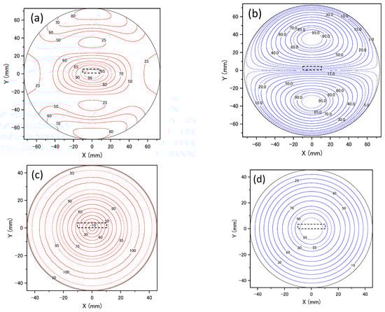
Figure 2.
Distribution of electromagnetic field in a cavity for the TM110 magnetic field (a), TM110 electric field (b), TM010 magnetic field (c), and TM010 electric field of (d). The black dashed lines indicate the sizes of the samples placed in the centers of the cavities.
The field strengths in the contour maps were standardized so that the highest and lowest values are 100 and 0, respectively. The highest strength of the magnetic field is in the center of the cavity (Figure 2a, X = 0 mm, Y = 0 mm), whereas the highest strengths of the electric field are at X = 0 mm and Y = ±36.6 mm (Figure 2b).
The sample to be heated consisted of a transistor and a substrate. The dimensions of the sample were W × D × H = 7.5 × 19 × 3 mm. The black dashed lines in Figure 2a,b indicate the sizes of the samples placed in the center of the cavities. The position of the solder paste was 1 mm in the Y direction from the center of the cavity because the thickness of the substrate was 1 mm. The field strengths of the magnetic field and electric field at a distance of 1 mm in the Y direction were 95–100 and 0–5, respectively. The field strengths of the magnetic field and electric field at the position where the transistor was to be placed at Y = 2–3 mm where 95–97.5 and 5–10, respectively.
Figure 2c,d show the distributions of the strengths of the magnetic and electric fields produced by the TM010 microwave resonator, which was used to compare magnetic field heating. These figures facilitated determination of the strengths of the electromagnetic fields at the positions of the samples. The maximum strength of the magnetic field was at a position on the circumference at a distance of 37 mm from the center of the cavity. The maximum strength of the electric field was in the center (X = 0 mm, Y = 0 mm) of the cavity.
The field strengths of the magnetic field and electric field at a distance of 1 mm in the Y direction were 0–45 and 92.5–100, respectively. A sample placed at the center of the cavity was therefore exposed to a strong electric field.
4.2. Soldering of a Transistor by Magnetic Field Heating
The samples were heated by microwave irradiation using the TM110 magnetic field. Figure 3 shows that the appearance of the sample before microwave irradiation (Figure 3a), an infrared camera image of the sample during microwave heating (3b), and the temperature of the sample (upper) and power of the radiation (bottom) as a function of time (3c).
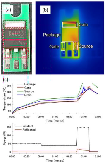
Figure 3.
Photograph of sample (a) and thermal image of sample heated in a TM110 cavity (b), and temperature (top) and power (bottom) profile for microwave heating in a TM110 cavity (c). Dashed red lines in (a) indicate positions where temperatures were calculated. Rectangles outlined by solid white lines in (b) indicate regions where temperatures were highest.
A video of the thermo and optical images during microwave heating can be found in the Supplementary Data (Video S1). The positions of the calculated temperature (package, gate, source, and drain) are indicated by the rectangles outlined by red dashed lines in the photograph (Figure 3a). To calculate temperatures, the emissivity at each position of the package, gate, source, and drain were set to 0.65, 0.44, 0.44, and 0.44, respectively. Temperatures were highest within the rectangles outlined by solid white lines in Figure 3b.
Figure 3c shows the temporal variation in the temperature at each position and the microwave power (incident and reflected). The heating temperature was controlled by manually controlling the incident microwave power. The heating was performed within the time required for removal of the oxide layer of the solder by the flux and for soldering, approximately 1 min and 30 s, respectively. The microwave power was input at 40–50 W for the flux activation. For the melting of solder paste, the power was increased to 150 W, and the temperature of the joint increased to 220 °C. The profiles of power versus time for incident and reflected radiation indicate that microwave energy was efficiently confined in the cavity because the reflected power was small.
During microwave heating, the temperatures of the positions of the source and package were highest and lowest, respectively. In the magnetic field, the solder paste was therefore selectively heated. The position of the source was heated the most.
There were two metal parts in the samples, the solder paste and the outer lead. The solder paste was heated more than the outer lead. We hypothesized that this difference was due to surface area differences. The solder paste consisted of small solder particles (approximately 35 μm in diameter, type 4) and was larger than the area of the outer lead. For induction heating, the heat generated by eddy currents depends on the surface area of the metal because of the relationship between skin depth and power dissipation [12]. The solder paste with its large metallic surface area was heated more than the outer lead with its small metallic surface area.
4.3. Soldering of a Transistor by Electric Field Heating
By using the TM010 mode cavity, the sample was heated by microwave irradiation in an electric field. Figure 4 shows the appearance of the sample before microwave irradiation (4a), a thermo camera image (4b) of sample during microwave heating, and the temperature profile (4c). In addition, a video of the thermo and optical image during microwave heating is available as Supplementary Data (Video S2). To calculate temperatures, emissivity at each position where package, gate, source, drain, and circuit board (CB) was set as 0.65, 0.44, 0.44, 0.44, and 0.61, respectively.
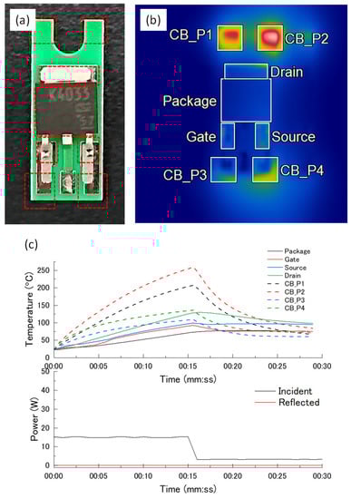
Figure 4.
Photographic image of sample (a) and thermal image of sample heated in a TM010 cavity (b), and temperature (upper) and power (bottom) profiles over time for microwave heating in a TM010 cavity(c). The positions of the calculated temperature are shown as red dashed rectangles in (a). Temperatures were highest in the range of each white rectangle in (b).
When inputting 15 W of microwave power, two positions (CB_P1 and CB_P2) on the circuit board were selectively heated without heating at the target positions (gate, source, and drain). Microwave irradiation was stopped at 15 s because of selective heating at the two positions. For electric field heating, we hypothesized that a cause of the overheating was the presence of the copper foil exiting as a heat spreader inside of the circuit board. With microwave heating, electromagnetic wave energy is concentrated on the edge of the conductive material, and abnormal heating is often observed. In microwave heating using TM010, it is impossible to inject microwave energy at the target positions due to the concentration of the microwave energy on the edge of the metal. Consequently, it is difficult to raise the temperature of the solder paste to the melting point.
4.4. Observation of Cross Section of the Sample
Figure 5a shows the appearance of the sample in which the transistor was bonded to the substrate by magnetic field heating, and Figure 5b,c shows a cross section of the junction. The numbers in Figure 5a indicate the positions where the cross section was observed. The fillet could be confirmed at the joint of the drain (Figure 5b, position 1) and the gate (Figure 5c, position 2). There were almost no bubbles inside the fillet. The outer lead and the substrate were therefore joined well.
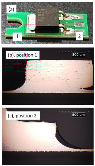
Figure 5.
Exterior image of a sample heated by a magnetic field (a) and digital microscope images of the junctions (b,c).
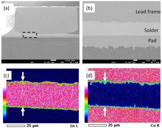
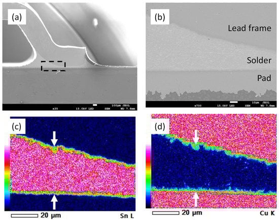
Figure 6 and Figure 7 show that SEM images and EDS mapping images of the sample confirming the alloy phase of the solder joints at the position 1 and 2 in Figure 5. The solder spread between the lead frame and the pad, and no voids were observed in the solder (Figure 6b and Figure 7b). In EDS mapping images (Figure 6c and Figure 7c) of tin (Sn), it was confirmed that layers with low concentration of tin (the part indicated by the white arrows) above and below the solder layer. EDS mapping images of copper (Cu) are shown in Figure 6d and Figure 7d. Layers of low concentration of Cu were formed at the interface among the lead frame, pad, and solder, as indicated by the white arrows. The coincidence of the locations of the layers with low concentrations of Sn and Cu indicated the formation of a Sn–Cu alloy phase at the interfaces.
4.5. Evaluation of Transistor Characteristics
To investigate the effects of microwave heating on the transistor, we examined the output and transfer characteristics of the transistor (Figure 8). The measurements were performed by probing to the terminal of the adapter board. The output characteristics of the sample after microwave heating (Figure 8a) revealed a drain current of 33 mA at a gate voltage of 2.25 V. The drain current obtained from the transistor before microwave heating was 21 mA. Microwave heating therefore caused the drain current to increase. We hypothesized that this effect was caused by the fact that the heat received by the lead frame during microwave heating was transferred to the transistor, and the semiconductor in the transistor was annealed.
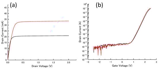
Figure 8.
Characteristic curves after microwave heating (red) and before microwave heating (black) of output characteristic (a) and transfer characteristic (b).
The transfer characteristics (Figure 8b) did not differ between before and after microwave heating. The semiconductor characteristics obtained from the transfer curve had a gate voltage threshold of about 2.5 V, which did not differ from the manufacturer’s recommended value.
A MOSFET was repeatedly prepared by heating with a magnetic field, and its performance was evaluated. There was no significant effect of microwave heating on the performance of the MOSFET (Table 1).

Table 1.
Summary of characteristic values of MOSFET after microwave heating.
4.6. Comparison of Shear Strength between Microwave Heating and Conventional Reflow
To compare between the microwave and conventional reflow, a difference of shear strength was evaluated.
A heating condition for the conventional reflow was carried as follows: the sample was heated in an electric furnace at 140 °C for 3 min for flux activation, and then heated at 260 °C for 2 min for soldering. Although it was heated with the same heating profile as the microwave heating, the solder paste was not melted.
Good bonding was confirmed from the optical images (Figure 9).
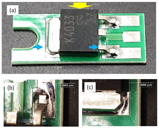
Figure 9.
Exterior image of a sample soldered by the conventional reflow. Appearance (a) and magnified view (b,c) of indicated position in Figure 1a by the blue arrows. A yellow arrow indicates a direction of the shear test.
Shear strengths were 68.559 and 64.598 kgf for the microwave and conventional reflow samples, respectively (a direction of a load for the shear test is indicated in Figure 9). There was no significant difference in shear strength due to differences in heating methods.
5. Conclusions
In this study, we compared the effects of heating solder with microwave irradiation in a magnetic field and an electric field. To estimate the field strengths of the magnetic field and electric field in advance, we numerically simulated the fields of the TM110 and TM010 microwave resonators. The sample (W × D × H = 7.5 × 19 × 3 mm) positioned at the center of the cavity of the TM110 microwave resonator was exposed to 95–100% and 0–5% of the strength of the magnetic field and electric field, respectively. The sample positioned at the center of the cavity of the TM010 microwave resonator was exposed to 0–45% and 92.5–100% of the strength of the magnetic field and electric field, respectively. Use of the TM110 mode cavity resulted in heating of the solder with suppression of discharge because the magnetic field was strongest and the electric field weakest at the heating position.
Based on the simulation, the sample was heated using the TM110 and TM010 cavities. In the case of the TM110 mode cavity, the transistor was jointed on the PCB with solder heated with microwave irradiation for 1 min, 30 s. The condition of the joint between the PCB and lead frame via solder was good because Sn–Cu alloy phase was formed. In the comparison between microwave and conventional reflow, there was no difference in bonding strength due to the difference in heating mode. The position of the transistor was heated, in ascending order, from the source, drain, gate, and package. When the TM010 mode cavity was used, the edges of the PCB were selectively heated. It was impossible to heat the solder paste set around the transistor. The undesirable positions of the PCB were selectively heated when the TM010 mode cavity was used and it was impossible to heat the solder paste set around the transistor.
To evaluate the effect of microwave heating on the transistor, we assessed the output and transfer characteristics of the transistor. We discovered that irradiation increased the output current. With respect to its transfer characteristics, we found that the transistor operated normally without any change in the gate voltage.
Clearly, from these results, to mount electronic components using microwave heating, microwave irradiation using a magnetic field is important. We obtained broadly applicable knowledge that can be used in the future for mounting other electronic components.
Supplementary Materials
The following supporting information can be downloaded at: https://www.mdpi.com/article/10.3390/pr11020491/s1, Video S1: Mounting of a sensor by microwave heating in magnetic field. Video S2: Mounting of a sensor by microwave heating in electric field.
Author Contributions
Conceptualization, T.N., M.N., S.U., K.T., H.Y. and H.S.; methodology, T.N., M.N. and S.U.; validation, T.N.; formal analysis, T.N.; investigation, T.N.; resources, T.N., M.N., S.U., K.T., H.Y. and H.S.; data curation, T.N.; writing—original draft preparation, T.N.; writing—review and editing, T.N. and K.T.; visualization, T.N.; supervision, T.N.; project administration, T.N. and K.T.; funding acquisition, K.T. and H.S. All authors have read and agreed to the published version of the manuscript.
Funding
This research was funded by a research fund from Senju metal industry.
Institutional Review Board Statement
Not applicable.
Informed Consent Statement
Not applicable.
Data Availability Statement
Not applicable.
Conflicts of Interest
All support for the present manuscript such as editing, article processing charges was received a research grant from AIST. K. Tomitsuka, H. Yoshida, and H. Sakuma are employees of Senju metal industry. The authors have no competing interests to disclose excepting described above.
References
- Arunasalam, M.; Leman, Z.B.; Baharudin, B.; Sulaiman, S.B.; Das, C.S.A. Challenges in minimizing copper dissolution for lead free wave soldering in surface mount technology going towards green manufacturing. Int. J. Precis. Eng. Manuf. Green Technol. 2022, 9, 645–660. [Google Scholar] [CrossRef]
- Jacobson, D.M.; Harrison, M.R. Lead-free soldering: A progress report. Gec. J. Technol. 1997, 14, 98–109. [Google Scholar]
- Nowottnick, M.; Diehm, R. Soldering technology for 3D PCB assemblies with microwave heating. In Proceedings of the IEEE International Symposium on Industrial Electronics, Vigo, Spain, 4–7 June 2007; p. 3273. [Google Scholar]
- Nowottnick, M.; Scheel, W.; Pape, U.; Diehm, R.; Wiese, J.; Kempe, W.; Mallah, M.; Suppa, M.; Fink, P. Solder pastes for microwave application. In Proceedings of the 2006 1st Electronic Systemintegration Technology Conference, Dresden, Germany, 5–7 September 2006; p. 415. [Google Scholar]
- Moon, K.S.; Li, Y.; Xu, J.W.; Wong, C.P. Lead-free interconnect technique by using variable frequency microwave. J. Electron. Mater. 2005, 34, 1081–1088. [Google Scholar] [CrossRef]
- Xu, H.B.; Li, M.Y.; Fu, Y.G.; Wang, L.; Kim, J. Local melt process of solder bumping by induction heating reflow. Solder. Surf. Mt. Technol. 2009, 21, 45–54. [Google Scholar] [CrossRef]
- Yusof, F.; Idris, S. Investigating Sn-Ag-Cu (SAC) solder bump joints produced using modulated pulse laser soldering. Laser Eng. 2021, 51, 347–354. [Google Scholar]
- Jaya, N.T.; Idris, S.R.A.; Ishak, M. A review on mechanical properties of SnAgCu/Cu joint using laser soldering. In Proceedings of the 3rd International Conference on Mechanical, Manufacturing and Process Plant Engineering (ICMMPE), Batu Ferringhi, Malaysia, 22–23 November 2017; pp. 97–107. [Google Scholar]
- Kanazawa, K.; Nakamura, T.; Nishioka, M.; Uemura, S. Investigation of the thermal properties of electrodes on the film and its heating behavior induced by microwave irradiation in mounting processes. Processes 2020, 8, 557. [Google Scholar] [CrossRef]
- Miyakawa, M.; Nakamura, T.; Iwabuchi, R.; Nishioka, M. Sheet-type flow process using magnetic-field-induced heating with single-mode microwaves applied to a continuous metal nanoparticle synthesis. Ind. Eng. Chem. Res. 2020, 59, 20447–20454. [Google Scholar] [CrossRef]
- Metaxas, A.C. Foundations of Electroheat: A Unified Approach; Wiley: West Sussex, UK, 1996. [Google Scholar]
- Yoshikawa, N.; Ishizuka, E.; Taniguchi, S. Heating of metal particles in a single-mode microwave applicator. Mater. Trans. 2006, 47, 898–902. [Google Scholar] [CrossRef]
Disclaimer/Publisher’s Note: The statements, opinions and data contained in all publications are solely those of the individual author(s) and contributor(s) and not of MDPI and/or the editor(s). MDPI and/or the editor(s) disclaim responsibility for any injury to people or property resulting from any ideas, methods, instructions or products referred to in the content. |
© 2023 by the authors. Licensee MDPI, Basel, Switzerland. This article is an open access article distributed under the terms and conditions of the Creative Commons Attribution (CC BY) license (https://creativecommons.org/licenses/by/4.0/).