Article

Sub-ppm NO2 Detection through Chipless RFID Sensor Functionalized with Reduced SnO2

1
Center for Sensors and Devices, Fondazione Bruno Kessler, 38123 Trento, Italy
2
Department of Information Engineering and Computer Science, University of Trento, 38123 Trento, Italy
3
Department of Civil Environmental and Mechanical Engineering, University of Trento, 38123 Trento, Italy
*
Author to whom correspondence should be addressed.
Chemosensors 2023, 11(7), 408; https://doi.org/10.3390/chemosensors11070408
Submission received: 29 April 2023 / Revised: 5 July 2023 / Accepted: 13 July 2023 / Published: 20 July 2023

Abstract

:
NO2 is an important environmental pollutant and is harmful to human health even at very low concentrations. In this paper, we propose a novel chipless RFID sensor able to work at room temperature and to detect sub-ppm concentration of NO2 in the environment. The sensor is made of a metallic resonator covered with NO2-sensitive tin oxide and works by monitoring both the frequency and the intensity of the output signal. The experimental measurements show a fast response (a few minutes) but a very slow recovery. The sensor could therefore be used for non-continuous threshold monitoring. However, we also demonstrated that the recovery can be strongly accelerated upon exposure to a UV source. This opens the way to the reuse of the sensor, which can be easily regenerated after prolonged exposure and recycled several times.

1. Introduction

Nitrogen dioxide (NO2) is a well-known environmental pollutant which is emitted in large quantities from high-temperature combustion processes in cars, furnaces and power plants. The Recommended Exposure Limit-Short Term Exposure Limit (REL-STEL) for NO2 is 1 ppm, owing to its significant harmful effect on human health even at very low concentrations [1]. For this reason, NO2 detection at sub-ppm concentrations is especially important for pollution control, and many types of gas-sensing systems have been developed for its detection, including electrochemical, optical and chemiresistive sensing. Among the various types of gas sensors, the metal oxide semiconductor (MOS) gas sensor shows high responsivity, fast response and recovery times and a vast choice of semiconductor metal oxides as gas-sensitive layers [2,3,4].
However, even though recently materials working at low temperature have been proposed in the literature [2,5,6], the usual MOS-based gas sensor operates at temperatures in the range of 200–500 °C and in DC mode [5,6,7]. These are important drawbacks that limit the exploitation of these devices in many sensing applications. In particular, the need for an external bias source, dedicated wiring and a micro-heating structure for thermoactivating the nanostructured MOS results in an increase in the cost and the complexity of the sensing system. In the upcoming scenario of the increased wireless system integration of the Internet of Things (IoT), with the emerging needs for ubiquitous sensing and identification of objects, these difficulties play an important role in limiting the technological exploitation and market uptake of environmental gas sensors.
A promising solution to overcome these intrinsic limitations of traditional MOS sensors can be found in the exploitation of a different transduction mechanism [8,9], while at the same time maintaining the excellent material sensitivity of metal-oxides. A good opportunity to address this challenge is the replacement of MOS sensors with microwave sensors [10], in order to have a seamless integration of the sensing capability and the wireless transduction of the signal.
Microwave sensors [11] exhibit good long-term stability, work preferentially at room temperature and can be read wirelessly. A variety of sensor designs and reading architectures have been reported in the literature, including metamaterial-based resonators and resonator arrays [12], UHF tags [13], chipless radio frequency identification (RFID) sensors [14,15] and piezoelectric surface acoustic wave detectors [16]. The electrical signal can be experimentally detected in terms of frequency, phase or insertion loss and correlated to the quantification of the parameter that caused the variation. In particular, chipless RFID technologies became very attractive [17] with the advent of the IoT platform and have been already exploited in several applications, going from supply chain management, logistics and storage of goods [18]. Together with the tracking ID function, the chipless RFID sensor can provide an additional sensing capability with benefits in terms of cost, compactness, robustness and lower radiated power. Examples of chipless RFID sensors are already been reported in several domains [19], such as temperature [20], humidity [21,22], pH [23] and strain and gas sensing [24], and the use of a suitable smart sensing material [23] is often the key for their competitive performance.
In this paper, we propose a microwave-based sensor approach in order to address this challenge. This microwave-based NO2 sensor is a dual parameter sensor that can operate by reading the variations of both the intensity and the frequency of the peak signal. The physical structure is made of a metallic microwave resonator covered with a metal-oxide sensitive material. The frequency and intensity changes can be read remotely without direct electric contact. The chipless RFID approach of this sensing structure is particularly interesting for long-term environmental measurements because it does not require batteries on the sensor, which is consequently completely passive. Moreover, the sensor can be easily inserted in a more complex tag structure associated with identification resonators, in order to become a complete chipless RFID sensor.
Regarding the choice of the sensing material, various MOS have been proposed so far for NO2 detection [25,26,27,28,29], and among them, tin dioxide (SnO2) highlighted interesting detection features [30,31,32,33]. In particular, the introduction of high oxygen vacancy (VO) concentrations on the SnO2 nanostructures results in a strong improvement of sensing performance in the detection of oxidizing gases [34]. In fact, in such a condition, oxidizing gases such as NO2 tend to interact directly with the surface oxygen vacancies of the nanostructures, by oxidizing them, resulting in a strong change of the SnO2 electrical resistance even at room temperature [34,35]. Several approaches have been used so far to introduce controlled types (bulk or surface) and concentrations of oxygen vacancies into MOS nanostructures, including chemical synthesis, ion bombardments or heat treatments in reducing atmosphere [35]. In this work, the oxygen vacancies were introduced in the SnO2 nanoparticles through a heat treatment in a reducing atmosphere (N2/H2: 95/5) obtaining a material which is extremely sensitive to NO2 environmental concentration.
The combination of a high-performing material with an innovative sensor transduction technology allows us to demonstrate the wireless detection of NO2 environmental concentration at the sub-ppm level at room temperature.

2. Materials and Methods

2.1. Chipless RFID Resonator Structure

The sensor is composed of a metallic sensing structure over a flexible low-loss substrate, covered by a thin layer of reduced SnO2 nanoparticles. The geometry of the metallic structure is that of an Electric-field coupled (ELC) resonator [36,37]. The design and the simulation of this structure are reported in detail in [21], but the whole structure was scaled in order to have the first resonant peak around 1.78 GHz. The structure and its geometrical dimensions are schematized in Figure 1. The important difference compared to [21] is that the resonating structure is not coupled to a microstrip transmission line but is remotely read with an electromagnetic probe, as in [38,39]. This last arrangement allows the resonator to be read wirelessly with a commercial circular electromagnetic probe [40] without amplification. The selected probe has a diameter of 20 mm.
The metallic structure was realized by microlithography on a flexible 168 µm-thick RO4350 Rogers substrate, covered with 17 µm of copper. The copper was defined by microlithography and then wet-etched.

2.2. Sensing Material Synthesis, Characterization and Deposition

SnO2 nanoparticles were synthesized through the sol-gel method. Tin(II) 2-ethylhexanoate [0.1 M] was dissolved in 100 mL of a hydroalcoholic solution (propanol/water 70/30%). The gel formed was left to decant overnight. Afterwards, the gel was separated from the sol by filtration and then dried at 100 °C for 6 h and calcined for 2 h at 650 °C, in order to obtain stoichiometric SnO2 nanoparticles. To create oxygen vacancies, SnO2 nanoparticles were then heat treated at 600 °C for 30 min in a reducing atmosphere (H2/N2 5/95%). The reducing heat treatment was followed by a vacuum heat treatment at 600 °C for 15 min, useful to stabilize the structure of reduced SnO2 (SnO2-VO) nanoparticles. This final processing step is necessary because otherwise, they tend to be easily re-oxidized by O2 and H2O present in the air once the SnO2-VO material is exposed to the room atmosphere [35].
The morphology and composition of both stoichiometric SnO2 and SnO2-VO nanoparticles were characterized using a Zeiss Leo 1530 Gemini (Zeiss, Oberkochen, Germany) Scanning Electron Microscope (SEM), equipped with an X-ray Energy Dispersive Spectrometer (EDS). The powders were deposited on carbon tape placed on top of suitable specimen stubs for SEM analysis. The analysis of SEM images was performed using a suitable image processing program (ImageJ, National Institutes of Health and the Laboratory for Optical and Computational Instrumentation, University of Wisconsin, Madison, WI, USA).
The optical absorption of the two nanopowders was investigated using a Jasco V-670 spectrophotometer (Jasco International Co., Ltd., Tokyo, Japan). The samples were dispersed in 2-propanol and transferred into quartz cuvettes with an optical path of 1 cm. Absorption spectra were collected in the wavelength range of 200–800 nm. The bandgap of the samples was calculated by using the Tauc method.
X-ray photoelectron spectroscopy measurements were performed using a Kratos AXIS UltraDLD instrument (Kratos Analytical, Manchester, UK) equipped with a hemispherical analyzer and a monochromatic X-ray source Al Kα (1486.6 eV), in spectroscopy mode. The powders were deposited on carbon tape placed over a silicon support. Samples were analyzed using a 0° take-off angle between the sample surface normal and the analyzer axis. High-resolution spectra of the core levels of O 1s, C 1s and Sn 3d were collected for each sample. The alignment was performed by setting the hydrocarbon peak in the C 1s core level peak at 285 eV. XPS data were analyzed using the software described elsewhere [41].
To be applied as sensing material over the resonating structure, the SnO2-VO nanoparticles have been suspended in a 2-propanol solution and then deposited as a thin film over the metallic resonator by spin coating.

2.3. Test Bench Setup and RF Measurements

The sensing performance of the SnO2-VO RFID sensor was characterized by using a dedicated apparatus, including a custom-made gas-flow test chamber (500 cm3) coupled with an Agilent E5061B ENA Vector Network Analyzer (VNA). A schematic representation of the apparatus is depicted in Figure 2.
Gas sensing measurements were performed at room temperature (20 ± 2 °C) by exposing the sensing film to controlled gaseous mixtures. Synthetic air (20% O2 and 80% N2) and target gas (NO2) were fluxed and mixed from certified cylinders (N5.0 degree of purity) through calibrated mass-flow controllers (MFC), achieving a constant total flow of 500 sccm. The lowest NO2 concentration which is possible to inject into the gas chamber was 0.5 ppm, which is half of the REL-STEL concentration. The relative humidity was monitored by a digital humidity sensor (1.0% accuracy) located at the chamber exit. Relative humidity control was achieved by injecting a fixed fraction of the total dry air flux into a gas bubbler filled with deionized water to create the desired humidity conditions [33]. The control of the environmental humidity is considered essential for a reproducible measurement because there are indications in the literature that this type of sensing material can be sensitive to humidity [22].
The radio-frequency (RF) measurements were taken from 1.5 to 2.0 GHz, with a sampling interval of 0.35 MHz. The sensing circular probe, which monitors the frequency and intensity variations of the resonator through the measurement of the return loss, is not depicted in Figure 2, due to its small dimensions. During the experiment, it was directly connected to the VNA, as shown in Figure 3. The sensor tag was located face-down inside the custom-made test chamber, where the gas environment was controlled, while the probe was kept outside, and the detection was performed through the plastic chamber wall (~1 mm) and the sensing tag substrate. The sensor tag located face-down maximizes and makes faster the interaction between the tag and the gas in the chamber.
In order to speed up the sensor recovery, an UV LED (ultra-violet light emitting device) was used, with a central wavelength of 405 nm. The LED power was kept low (around 1 mW) to avoid heating effects on the sensor. The LED was positioned inside the test chamber, as shown in Figure 3.

3. Results and Discussion

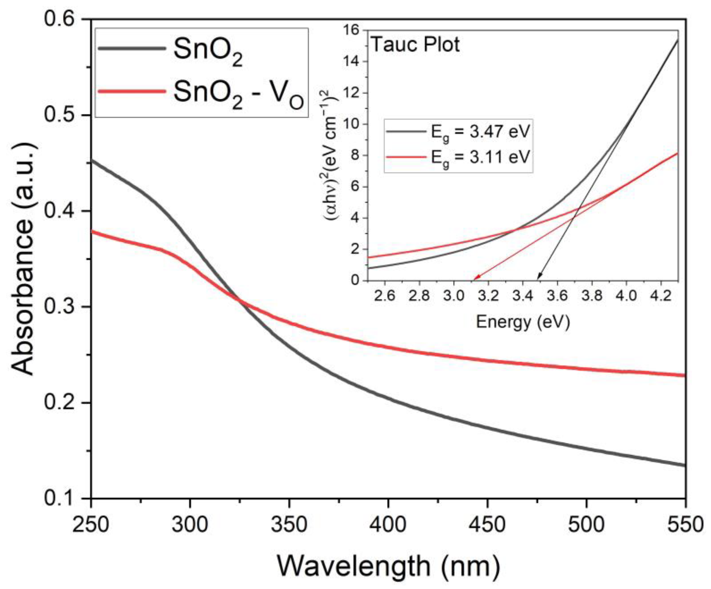
3.1. Sensing Material Characterization

The effect of thermal processing on the formation of oxygen vacancies in SnO2 nanopowders was studied in detail. SEM characterization was used to compare the morphology of the stoichiometric SnO2 and SnO2-VO samples (Figure 4a,b). It is evident that both samples present nanoparticles with a spherical-like morphology, suggesting that the thermal processing did not alter the shape of the nanoparticles.
The analysis of SEM images revealed that the average nanoparticle size was approximately 29 nm for stoichiometric SnO2 and 19 nm for SnO2-VO. This decrease in nanoparticle size due to the incorporation of oxygen vacancies in the metal oxide lattice has been observed in prior studies [42,43] and may be caused by doping effects of the VO in the SnO2 crystal lattice.
EDS was used to analyze the Sn/O ratio of the nanopowder before and after the reducing thermal treatment. The results revealed that the Sn/O ratio increased from 0.52 (for stoichiometric SnO2) to 0.55 for SnO2-VO, indicating a significant decrease in the relative oxygen content of the nanopowder. This is attributed to the reducing heat treatment, which caused the oxygen molecules to be removed from the SnO2 structure.
The formation of VO in the nanoparticles due to the reducing thermal treatment was also investigated by characterizing the optical properties of stoichiometric SnO2 and SnO2-VO. In particular, the implementation of bulk VO in a crystalline metal oxide should involve a band gap narrowing compared to the stoichiometric semiconductor, due to the doping effect of the oxygen vacancies that behave as defects in the crystal structure, leading to the shift of the Fermi level towards the conduction band as well as the creation of mid-gap donor states that may overlap with the electronic states at the conduction band and/or valence band edges [44,45]. The optical absorption spectra of stoichiometric SnO2 and SnO2-VO nanopowders, collected by means of a UV–vis spectrometer, are shown in Figure 5.
The energy of the direct band gap (Eg) for the two materials (inset of Figure 4) was estimated employing the Tauc method [46]. The calculated bandgaps were 3.47 and 3.11 eV for stoichiometric SnO2 and SnO2-VO, respectively. The narrowing in the bandgap further demonstrated the formation of oxygen vacancies in the SnO2 because of the reducing thermal treatment at 600 °C.
The high-resolution Sn 3d core level spectra for both stoichiometric SnO2 and SnO2-VO (Figure 6a) showed the presence of a doublet related to the Sn 3d3/2 (≈495.2 eV) and Sn 3d5/2 (≈486.8 eV) components. Due to the very similar binding energy of Sn2+ and Sn4+ in SnO and SnO2 [47], a deconvolution of Sn 3d3/2 and Sn 3d5/2 for the two samples is non-trivial. Nevertheless, high-resolution spectra showed a shift of both Sn 3d3/2 and Sn 3d5/2 peaks for the SnO2-VO sample compared to stoichiometric SnO2, which could be attributed to the formation of oxygen vacancies [47,48]. In addition, the Sn 3d spectrum of SnO2-VO sample showed the presence of another doublet with low intensity, located at 492.9 eV (Sn 3d3/2) and 484.4 eV (Sn 3d5.2), which can be attributed to Sn0, further demonstrating the reduction of SnO2 nanoparticle surface [48].
Figure 6b,c show the high-resolution spectra of O 1s core levels for SnO2 and SnO2-VO samples. Also in this case, a shift of the peak binding energy is observed in the two samples, similar to the shift observed for the Sn 3d peaks. The fit highlighted the presence of two peaks in both powders, located at 530.88 eV and 531.91 eV for stoichiometric SnO2 and 530.64 eV and 531.63 eV for SnO2-VO [49]. While the peak at lower binding energy is attributable to the oxygens of SnO2 lattice (Olattice), the peak at higher binding energy contains the contribution of both oxygen adjacent to oxygen vacancies (Ovac) and oxygens bonded to carbon residuals within the sample, whose similar binding energies make it difficult to further deconvolute it into two peaks [49,50]. Considering that the concentration of C-O is comparable in the two samples, a change in the intensity of the peak at higher binding energy with respect to the Olattice peak can be reasonably attributed to a variation in the concentration of oxygens adjacent to oxygen vacancies and therefore to a change in the concentration of the oxygen vacancies. Analyzing the Olattice/Ovac ratio of the two peak intensities, a relative increase of the peak related to the oxygen adjacent to the oxygen vacancies for the SnO2-VO sample with respect to SnO2 was observed. Indeed, the Olattice/Ovac ratio was 1.77 for stoichiometric SnO2 and 1.37 for SnO2, respectively. The increase in the relative peak intensity of Ovac for SnO2-VO sample further demonstrated the impact of the thermal reducing treatment on the formation of the oxygen vacancies.

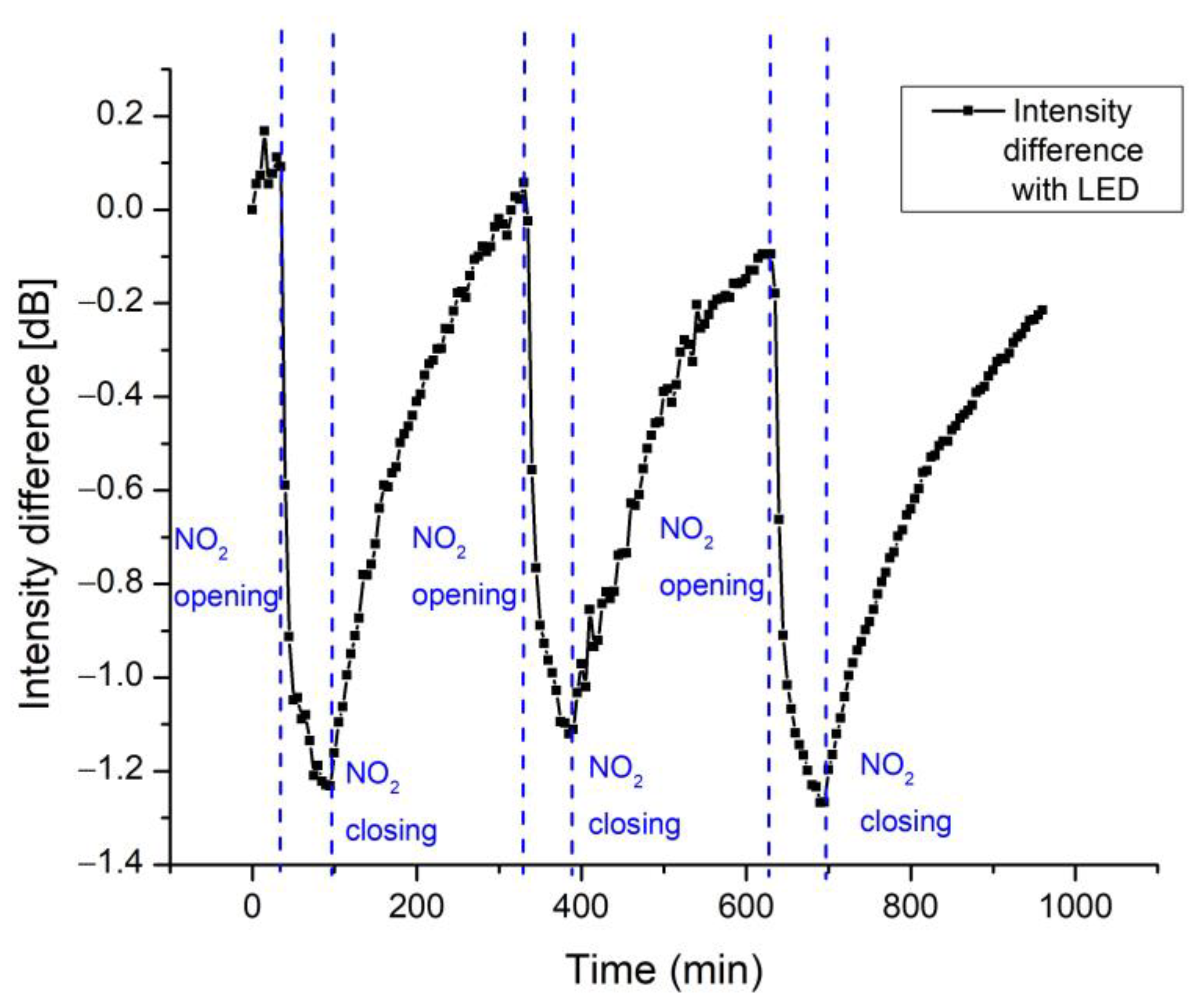
3.2. Performance of Chipless RFID Sensor

Since chipless RFID sensors can exploit both frequency and intensity changes, both parameters have been considered in order to assess the performance of the fabricated sensor for NO2 detection. Firstly, the frequency and the intensity of the resonator were monitored at three different values (0.5, 2.0 and 5.0 ppm) of NO2 concentration, to assess the sensing range. The relative humidity was kept at the fixed value of 50%, to eliminate the possible effects of the variation of this parameter on the measurements. The results obtained are reported in Figure 7 and Figure 8. Both the frequency and the intensity markedly change going from 0 to 0.5 ppm, while at concentrations higher than 2.0 ppm the sensor saturates. This reveals that the sensor is very sensitive at very low concentrations, in the range where the NO2 determination is more important and interesting for common applications. Moreover, the use of both parameters can make the determination more precise. It should be noted, however, that the intensity determination is more precise than the frequency shift. This was partially due to the limited frequency resolution of our measurement, which in this case is 0.35 MHz. This limit has been improved with an appropriate fitting of the experimental curves in the frequency interval of maximum peak intensity, which gave good results in terms of precision.
The error bars in Figure 8 have been calculated as the standard deviation on four measurements. In the case of frequency, the error bar was the larger value between standard deviation and frequency sampling, without taking into account the fitting improvement. The frequency-fitted data have been used in Figure 9, Figure 10 and Figure 11 and for the calculations of response and recovery times reported in the following.
It should be noted that, unlike the vast majority of the chipless sensors reported in the literature [14,21,51], in this specific case, the interaction of the pollutant with the sensing material causes an increase in the peak frequency and the Q-factor of the resonator. This is strictly related to the physico-chemical mechanism causing the sensing effect, that manifestly reduces both the loss and the dielectric constant of the sensing material, and is consistent with the conductivity reduction at increasing NO2 concentration observed in chemiresistive SnO2 sensors [52]. In fact, a lower SnO2 conductivity corresponds to a reduction of material losses and hence to a higher Q of the resonator, while the lower value of the dielectric constant may be caused by a reduction of charged defects (vacancies) in the chemical structure of the sensing material.
For a rough estimation of response and recovery times, a second measurement was performed after one day of waiting time. In this case, only the 0.5 ppm concentration was tested, but for longer times. The data acquired are reported in Figure 9 for both frequency and intensity. While the high sensitivity in the 0–0.5 ppm range is confirmed, it appears clearly that the response time of the sensor is much faster than the recovery time. The data reported in Figure 9 were tentatively fitted with a single exponential rise and decay curve.
The response/recovery times are then estimated as the times necessary to reach 90% of the total variation [53,54]. The results are reported in Table 1.
Even though the data reported in Table 1 are only rough estimates, it is clear that while the response time is in the order of minutes, the recovery time is in the order of several hours and may never be completed. Moreover, it is also possible that both the response and the recovery time are further slowed down at concentrations below 0.5 ppm.
The slow and incomplete recovery of the baseline shown in Figure 9 was previously observed in a similar device [20]. This behavior can be explained by the presence of reaction sites where target gas molecules may strongly bind at room temperature, inhibiting the complete desorption in the time scale of a sensing cycle.
With these characteristics, the sensor tag can be used as a (disposable) memory sensor for single-use exposure, maintaining the memory of the polluting event for a very long time, and is suitable for areas where the monitoring is not continuous. This use is conceivable due to the low cost of the tag itself. The lack of electronics on the tag makes the disposal less impactful for the environment and more suitable for harsh conditions when compared with other widely used sensors.
However, in view of the wider applicability of this technology and to promote the reusability of the whole system, we analyzed possible strategies to promote and speed up the sensor recovery. Among the different possibilities explored so far, the irradiation of the sensor with a UV LED gave encouraging results, because it allows the creation of electron-hole pairs while keeping the sensing device at room temperature, as well as the activation of the photocatalytic properties of the sensing material employed [27,55].
The data reported in Figure 10 and Figure 11 show the differences in the response and recovery trends with and without LED irradiation. The data show that the sensor behaves quite differently in these two cases.
The recovery time is strongly shortened upon LED irradiation (see Table 2), by almost one order of magnitude, and this is the most striking result of the UV exposure. In the case of irradiation, the recovery can be fully appreciated within the duration of the experiment, and therefore the recovery time is estimated more precisely compared to the recovery time without irradiation.
The irradiation also affects the time and the intensity of the sensor response. The estimations of the response times calculated as the time needed to reach 90% of the final value are reported in Table 2, and they are longer than without LED irradiation. However, from the curves in Figure 10 and Figure 11, it can be seen that the first and very fast part of the response curve is very similar in both cases, but without irradiation the response saturates after few minutes, while under UV exposure another (slower) process seems to take place, being visible in both the intensity and in the frequency response curve. The data are, however, not sufficient to separate the two trends.
Figure 12 reports the intensity change during three cycles under UV irradiation. The cycle includes one hour of exposure at 0.5 ppm of NO2 followed by three hours of recovery time. As can be seen, the UV irradiation does not degrade the material performance, and the repeatability is quite good.
Further tests at higher levels of NO2 evidenced that the sensor saturation level is not affected by the UV exposure and the behavior is very similar to that reported in Figure 8. In order to better appreciate the saturation point, the measurements were taken at 0.5, 0.75, 1, 1.5, 2 and 5 ppm. The saturation was found to be around 1.5 ppm, with the maximum sensitivity between 0 and 1 ppm. Results are reported in Figure 13 and compared with data in Figure 8.
Additional tests were performed to investigate the sensor sensitivity to CO because this is another important environmental pollutant that could interfere with NO2 determination. However, no variations of intensity and frequency have been detected, within the experimental error, for concentrations up to 10 ppm of CO.
While it is likely that the sensor is sensitive to environmental humidity, this dependence could be accounted for by coupling the sensor presented in this work with an additional chipless sensor sensitive only to humidity, as for instance those reported in [21,37].
The shortening of the recovery time is however the most important result because it opens the way to the reusability of the sensor. In its practical application, the sensor can be deployed for a long time without being monitored, then checked for NO2 exposure and finally restored with a UV source. A more powerful UV source can likely make the recovery even shorter than what has been measured in this work, but this possibility has not been explored yet, for concerns about the possible thermal effects on the sensor response.
Finally, it should be noted that even though the proposed chipless RFID sensor can be effectively considered a dual parameter sensor, the intensity variation turned out to be more precise and reliable than the frequency variation, even considering the frequency fit. It has been observed that this parameter shows some drift in very long measurements. The reasons for this behavior have not been understood completely yet, but they may be related to vibrations in the measurement set-up induced by the flowing in the tubing system, that progressively but invisibly changes the probe positioning relative to the measurement cell. This will be controlled more accurately in future experiments.
It is especially noteworthy that the NO2 concentration that can be detected at room temperature using the chipless sensor developed in this work is extremely low. In fact, the sensing characterization showed that the device is capable of detecting up to the lowest NO2 concentration injected into the gas chamber (i.e., 0.5 ppm), which is half of the REL-STEL concentration, paving the way for practical use of the sensor for NO2 detection for safety applications. The response shown at 0.5 ppm highlights the possibility to obtain a limit of detection of the photo-activated chipless sensor at even lower concentrations of NO2, opening up sub-ppm detection of NO2 useful in various application fields.

4. Conclusions

The chipless RFID sensor proposed in this work is extremely sensitive to low levels of NO2, at ambient temperature. Its sensitivity is highest in the range below 0.5 ppm, which is half of the REL-STEL limit. It shows a fast response and a slow recovery. These characteristics make it suitable for low-cost disposable threshold sensing in polluted environments. On the other hand, we have demonstrated that the recovery time can be shortened by UV-light irradiation by almost one order of magnitude, and this opens the way to the sensor reusability and consequent waste reduction. Future work will focus on understanding the mechanisms that control the sensor response and recovery at the chemical level, on the optimization of its performance in terms of reliability and response intensity and on the sensing characterization in the sub-0.5 ppm range.

Author Contributions

Conceptualization, V.M., A.G., M.V. and G.M.; methodology, V.M., A.G. and G.M.; software, M.V.; validation, M.V., L.L., M.D. and G.M.; formal analysis, V.M. and G.M.; investigation, M.V., M.D., L.V. and G.M.; resources, L.L. and M.D.; data curation, G.M.; writing—original draft preparation, V.M. and A.G.; writing—review and editing, V.M., A.G., M.D., M.V., L.V. and L.L.; visualization, V.M., L.V. and G.M.; supervision, M.D.; funding acquisition, L.L. and M.D. All authors have read and agreed to the published version of the manuscript.

Funding

This research received no external funding.

Institutional Review Board Statement

Not applicable.

Informed Consent Statement

Not applicable.

Data Availability Statement

The data presented in this study are available on request from the corresponding author.

Acknowledgments

The authors wish to thank Martino Bernard, Antonio Orlando, Guglielmo Trentini and Pietro Tosato for the technical support with the experimental set-up and LED technical installation. The authors wish to thank Soufiane Krik for the technical support in the development of the sensing materials used.

Conflicts of Interest

The authors declare no conflict of interest.

References

  1. NITROGEN DIOXIDE|Occupational Safety and Health Administration. Available online: https://www.osha.gov/chemicaldata/21 (accessed on 20 March 2023).
  2. Rydosz, A.; Brudnik, A.; Staszek, K. Metal Oxide Thin Films Prepared by Magnetron Sputtering Technology for Volatile Organic Compound Detection in the Microwave Frequency Range. Materials 2019, 12, 877. [Google Scholar] [CrossRef] [PubMed] [Green Version]
  3. Malik, R.; Tomer, V.K.; Mishra, Y.K.; Lin, L. Functional Gas Sensing Nanomaterials: A Panoramic View. Appl. Phys. Rev. 2020, 7, 021301. [Google Scholar] [CrossRef] [Green Version]
  4. Paleczek, A.; Grochala, D.; Staszek, K.; Wincza, K.; Gruszczynski, S.; Rydosz, A. Microwave-Based Nitrogen Dioxide Gas Sensor For Automotive Applications. In Proceedings of the 2021 International Conference on Electrical, Computer, Communications and Mechatronics Engineering (ICECCME), Réduit, Mauritius, 7–8 October 2021; pp. 1–4. [Google Scholar]
  5. Spagnoli, E.; Krik, S.; Fabbri, B.; Valt, M.; Ardit, M.; Gaiardo, A.; Vanzetti, L.; Della Ciana, M.; Cristino, V.; Vola, G.; et al. Development and Characterization of WO3 Nanoflakes for Selective Ethanol Sensing. Sens. Actuators B Chem. 2021, 347, 130593. [Google Scholar] [CrossRef]
  6. Gaiardo, A.; Bellutti, P.; Fabbri, B.; Gherardi, S.; Giberti, A.; Guidi, V.; Landini, N.; Malagù, C.; Pepponi, G.; Valt, M.; et al. Chemoresistive Gas Sensor Based on SiC Thick Film: Possible Distinctive Sensing Properties between H2S and SO2. Procedia Eng. 2016, 168, 276–279. [Google Scholar] [CrossRef]
  7. Neri, G. First Fifty Years of Chemoresistive Gas Sensors. Chemosensors 2015, 3, 1–20. [Google Scholar] [CrossRef] [Green Version]
  8. Gao, F.; Xuan, W.; Bermak, A.; Boussaid, F.; Tsui, C.-Y.; Luo, J. Dual Transduction on a Single Sensor for Gas Identification. Sens. Actuators B Chem. 2019, 278, 21–27. [Google Scholar] [CrossRef]
  9. Elnemr, Y.E.; Abu-Libdeh, A.; Raj, G.C.A.; Birjis, Y.; Nazemi, H.; Munirathinam, P.; Emadi, A. Multi-Transduction-Mechanism Technology, an Emerging Approach to Enhance Sensor Performance. Sensors 2023, 23, 4457. [Google Scholar] [CrossRef]
  10. Dey, S.; Saha, J.K.; Karmakar, N.C. Smart Sensing: Chipless RFID Solutions for the Internet of Everything. IEEE Microw. 2015, 16, 26–39. [Google Scholar] [CrossRef]
  11. Muñoz-Enano, J.; Vélez, P.; Gil, M.; Martín, F. Planar Microwave Resonant Sensors: A Review and Recent Developments. Appl. Sci. 2020, 10, 2615. [Google Scholar] [CrossRef]
  12. Schueler, M.; Mandel, C.; Puentes, M.; Jakoby, R. Metamaterial Inspired Microwave Sensors. IEEE Microw. 2012, 13, 57–68. [Google Scholar] [CrossRef]
  13. Singh, R.; Singh, E.; Nalwa, H.S. Inkjet Printed Nanomaterial Based Flexible Radio Frequency Identification (RFID) Tag Sensors for the Internet of Nano Things. RSC Adv. 2017, 7, 48597–48630. [Google Scholar] [CrossRef] [Green Version]
  14. Mulloni, V.; Donelli, M. Chipless RFID Sensors for the Internet of Things: Challenges and Opportunities. Sensors 2020, 20, 2135. [Google Scholar] [CrossRef] [PubMed] [Green Version]
  15. Patre, S.R. Passive Chipless RFID Sensors: Concept to Applications—A Review. IEEE J. Radio Freq. Identif. 2022, 6, 64–76. [Google Scholar] [CrossRef]
  16. Devkota, J.; Ohodnicki, P.R.; Greve, D.W. SAW Sensors for Chemical Vapors and Gases. Sensor 2017, 17, 801. [Google Scholar] [CrossRef] [PubMed] [Green Version]
  17. Ahmadihaji, A.; Izquierdo, R.; Shih, A. From Chip-Based to Chipless RFID Sensors: A Review. IEEE Sens. J. 2023, 23, 11356–11373. [Google Scholar] [CrossRef]
  18. Herrojo, C.; Paredes, F.; Mata-Contreras, J.; Martín, F. Chipless-RFID: A Review and Recent Developments. Sensors 2019, 19, 3385. [Google Scholar] [CrossRef] [Green Version]
  19. Karmakar, N.C.; Amin, E.M.; Saha, J.K. Chipless RFID Sensors; Wiley: Hoboken, NJ, USA, 2016. [Google Scholar]
  20. El Matbouly, H.; Tedjini, S.; Zannas, K.; Duroc, Y. Chipless RFID Threshold Temperature Sensor Compliant with UHF and ISM Radio Frequency. In Proceedings of the 2018 2nd URSI Atlantic Radio Science Meeting (AT-RASC), Gran Canaria, Spain, 28 May–1 June 2018; pp. 1–4. [Google Scholar]
  21. Marchi, G.; Mulloni, V.; Manekiya, M.; Donelli, M.; Lorenzelli, L. A Preliminary Microwave Frequency Characterization of a Nafion-Based Chipless Sensor for Humidity Monitoring. In Proceedings of the 2020 IEEE SENSORS, Rotterdam, The Netherlands, 25–28 October 2020; pp. 1–4. [Google Scholar]
  22. Tao, B.; Feng, L.; Miao, F.; Zang, Y. High Sensitivity Chipless RFID Humidity Sensor Tags Are Based on SnO2/G Nanomaterials. Vacuum 2022, 202, 111126. [Google Scholar] [CrossRef]
  23. Amin, E.M.; Saha, J.K.; Karmakar, N.C. Smart Sensing Materials for Low-Cost Chipless RFID Sensor. IEEE Sens. J. 2014, 14, 2198–2207. [Google Scholar] [CrossRef]
  24. Lee, J.S.; Oh, J.; Jun, J.; Jang, J. Wireless Hydrogen Smart Sensor Based on Pt/Graphene-Immobilized Radio-Frequency Identification Tag. ACS Nano 2015, 9, 7783–7790. [Google Scholar] [CrossRef]
  25. Haiduk, Y.S.; Khort, A.A.; Lapchuk, N.M.; Savitsky, A.A. Study of WO3–In2O3 Nanocomposites for Highly Sensitive CO and NO2 Gas Sensors. J. Solid State Chem. 2019, 273, 25–31. [Google Scholar] [CrossRef]
  26. Morais, P.V.; Suman, P.H.; Silva, R.A.; Orlandi, M.O. High Gas Sensor Performance of WO3 Nanofibers Prepared by Electrospinning. J. Alloys Compd. 2021, 864, 158745. [Google Scholar] [CrossRef]
  27. Gaiardo, A.; Fabbri, B.; Giberti, A.; Guidi, V.; Bellutti, P.; Malagù, C.; Valt, M.; Pepponi, G.; Gherardi, S.; Zonta, G.; et al. ZnO and Au/ZnO Thin Films: Room-Temperature Chemoresistive Properties for Gas Sensing Applications. Sens. Actuators B Chem. 2016, 237, 1085–1094. [Google Scholar] [CrossRef]
  28. Su, P.-G.; Li, M.-C. Recognition of Binary Mixture of NO2 and NO Gases Using a Chemiresistive Sensors Array Combined with Principal Component Analysis. Sens. Actuators A Phys. 2021, 331, 112980. [Google Scholar] [CrossRef]
  29. Lou, C.; Wang, K.; Mei, H.; Xie, J.; Zheng, W.; Liu, X.; Zhang, J. ZnO Nanoarrays via a Thermal Decomposition–Deposition Method for Sensitive and Selective NO2 Detection. CrystEngComm 2021, 23, 3654–3663. [Google Scholar] [CrossRef]
  30. Zhou, L.; Hu, Z.; Wang, P.; Gao, N.; Zhai, B.; Ouyang, M.; Zhang, G.; Chen, B.; Luo, J.; Jiang, S.; et al. Enhanced NO2 Sensitivity of SnO2 SAW Gas Sensors by Facet Engineering. Sens. Actuators B Chem. 2022, 361, 131735. [Google Scholar] [CrossRef]
  31. Jeong, H.-S.; Park, M.-J.; Kwon, S.-H.; Joo, H.-J.; Song, S.-H.; Kwon, H.-I. Low Temperature NO2 Sensing Properties of RF-Sputtered SnO-SnO2 Heterojunction Thin-Film with p-Type Semiconducting Behavior. Ceram. Int. 2018, 44, 17283–17289. [Google Scholar] [CrossRef]
  32. Devabharathi, N.; Umarji, A.M.; Dasgupta, S. Fully Inkjet-Printed Mesoporous SnO2-Based Ultrasensitive Gas Sensors for Trace Amount NO2 Detection. ACS Appl. Mater. Interfaces 2020, 12, 57207–57217. [Google Scholar] [CrossRef]
  33. Feng, Z.; Gaiardo, A.; Valt, M.; Fabbri, B.; Casotti, D.; Krik, S.; Vanzetti, L.; Ciana, M.D.; Fioravanti, S.; Caramori, S.; et al. Investigation on Sensing Performance of Highly Doped Sb/SnO2. Sensors 2022, 22, 1233. [Google Scholar] [CrossRef]
  34. Krik, S.; Gaiardo, A.; Valt, M.; Fabbri, B.; Malagù, C.; Pepponi, G.; Casotti, D.; Cruciani, G.; Guidi, V.; Bellutti, P. Influence of Oxygen Vacancies in Gas Sensors Based on Metal-Oxide Semiconductors: A First-Principles Study. In Sensors and Microsystems, Proceedings of the 20th AISEM 2019 National Conference, Naples, Italy, 11–13 February 2019; Di Francia, G., Di Natale, C., Alfano, B., De Vito, S., Esposito, E., Fattoruso, G., Formisano, F., Massera, E., Miglietta, M.L., Polichetti, T., Eds.; Springer International Publishing: Cham, Switzerland, 2020; pp. 309–314. [Google Scholar]
  35. Al-Hashem, M.; Akbar, S.; Morris, P. Role of Oxygen Vacancies in Nanostructured Metal-Oxide Gas Sensors: A Review. Sens. Actuators B Chem. 2019, 301, 126845. [Google Scholar] [CrossRef]
  36. Pushkar, P.; Gupta, V.R. A Design Rule for an ELC Resonator. In Proceedings of the 2015 International Conference on Innovations in Information, Embedded and Communication Systems (ICIIECS), Coimbatore, India, 19–20 March 2015; pp. 1–4. [Google Scholar]
  37. Marchi, G.; Mulloni, V.; Acerbi, F.; Donelli, M.; Lorenzelli, L. Tailoring the Performance of a Nafion 117 Humidity Chipless RFID Sensor: The Choice of the Substrate. Sensors 2023, 23, 1430. [Google Scholar] [CrossRef]
  38. Mulloni, V.; Marchi, G.; Lorenzelli, L.; Donelli, M. Chipless RFID Sensing System for Precise Ethanol Determination in Alcoholic Solutions. Electronics 2022, 11, 735. [Google Scholar] [CrossRef]
  39. Marchi, G.; Zanazzi, E.; Mulloni, V.; Donelli, M.; Lorenzelli, L. Electromagnetic Modeling Strategy Supporting the Fabrication of Inkjet-Printed Chipless RFID Sensors. IEEE J. Flex. Electron. 2023, 2, 145–152. [Google Scholar] [CrossRef]
  40. EMC Near-Field Probe Set with 40 DB Wideband Amplifier. Signal Hound. Available online: https://signalhound.com/products/emc-near-field-probe-set-40-db-wideband-amplifier/ (accessed on 17 June 2023).
  41. Speranza, G.; Canteri, R. RxpsG a New Open Project for Photoelectron and Electron Spectroscopy Data Processing. SoftwareX 2019, 10, 100282. [Google Scholar] [CrossRef]
  42. Shao, M.; Liu, J.; Ding, W.; Wang, J.; Dong, F.; Zhang, J. Oxygen Vacancy Engineering of Self-Doped SnO2−x Nanocrystals for Ultrasensitive NO2 Detection. J. Mater. Chem. C 2020, 8, 487–494. [Google Scholar] [CrossRef]
  43. De, A.K.; Sinha, I. Synergistic Effect of Ni Doping and Oxygen Vacancies on the Visible Light Photocatalytic Properties of Ag2O Nanoparticles. J. Phys. Chem. Solids 2022, 167, 110733. [Google Scholar] [CrossRef]
  44. Dangi, R.; Basnet, B.; Pandey, M.; Bhusal, S.; Budhathoki, B.; Parajuli, K.; Tiwari, S.K.; Kafle, B.P. Effect of Oxygen Vacancy on the Crystallinity and Optical Band Gap in Tin Oxide Thin Film. Energies 2023, 16, 2653. [Google Scholar] [CrossRef]
  45. Mesoudy, A.E.; Machon, D.; Ruediger, A.; Jaouad, A.; Alibart, F.; Ecoffey, S.; Drouin, D. Band Gap Narrowing Induced by Oxygen Vacancies in Reactively Sputtered TiO2 Thin Films. Thin Solid Film. 2023, 769, 139737. [Google Scholar] [CrossRef]
  46. Suzuki, T.; Watanabe, H.; Ueno, T.; Oaki, Y.; Imai, H. Significant Increase in Band Gap and Emission Efficiency of In2O3 Quantum Dots by Size-Tuning around 1 Nm in Supermicroporous Silicas. Langmuir 2017, 33, 3014–3017. [Google Scholar] [CrossRef]
  47. Kang, Y.-G.; Kim, H.-J.; Park, H.-G.; Kim, B.-Y.; Seo, D.-S. Tin Dioxide Inorganic Nanolevel Films with Different Liquid Crystal Molecular Orientations for Application in Liquid Crystal Displays (LCDs). J. Mater. Chem. 2012, 22, 15969–15975. [Google Scholar] [CrossRef]
  48. Kwoka, M.; Krzywiecki, M. Impact of Air Exposure and Annealing on the Chemical and Electronic Properties of the Surface of SnO2 Nanolayers Deposited by Rheotaxial Growth and Vacuum Oxidation. Beilstein J. Nanotechnol. 2017, 8, 514–521. [Google Scholar] [CrossRef] [Green Version]
  49. Babu, B.; Neelakanta Reddy, I.; Yoo, K.; Kim, D.; Shim, J. Bandgap tuning and XPS study of SnO2 quantum dots. Mater. Lett. 2018, 221, 211–215. [Google Scholar] [CrossRef]
  50. Idriss, H. On the wrong assignment of the XPS O1s signal at 531–532 eV attributed to oxygen vacancies in photo- and electro-catalysts for water splitting and other materials applications. Surf. Sci. 2021, 12, 121894. [Google Scholar] [CrossRef]
  51. Amin, E.M.; Karmakar, N.C.; Jensen, B.W. Fully Printable Chipless RFID Multi-Parameter Sensor. Sens. Actuators A Phys. 2016, 248, 223–232. [Google Scholar] [CrossRef]
  52. Maeng, S.; Kim, S.-W.; Lee, D.-H.; Moon, S.-E.; Kim, K.-C.; Maiti, A. SnO2 Nanoslab as NO2 Sensor: Identification of the NO2 Sensing Mechanism on a SnO2 Surface. ACS Appl. Mater. Interfaces 2014, 6, 357–363. [Google Scholar] [CrossRef]
  53. He, K.; Jin, Z.; Chu, X.; Bi, W.; Wang, W.; Wang, C.; Liu, S. Fast Response–Recovery Time toward Acetone by a Sensor Prepared with Pd Doped WO3 Nanosheets. RSC Adv. 2019, 9, 28439–28450. [Google Scholar] [CrossRef]
  54. Arafat, M.M.; Dinan, B.; Akbar, S.A.; Haseeb, A.S.M.A. Gas Sensors Based on One Dimensional Nanostructured Metal-Oxides: A Review. Sensors 2012, 12, 7207–7258. [Google Scholar] [CrossRef]
  55. Chizhov, A.S.; Rumyantseva, M.N.; Vasiliev, R.B.; Filatova, D.G.; Drozdov, K.A.; Krylov, I.V.; Marchevsky, A.V.; Karakulina, O.M.; Abakumov, A.M.; Gaskov, A.M. Visible Light Activation of Room Temperature NO2 Gas Sensors Based on ZnO, SnO2 and In2O3 Sensitized with CdSe Quantum Dots. Thin Solid Film 2016, 618, 253–262. [Google Scholar] [CrossRef]
Figure 1. Scheme of the sensing structure. All the dimensions are in mm. The green zone is where the sensing material is deposited. All measures are in millimeters.
Chemosensors 11 00408 g001
Figure 2. Schematic representation of the gas mixing system composed of certified gas bottles, mass flow controller (MFC), bubbler for humidity control and sealed gas measurement chamber. Data acquisition is performed through a Vector Network Analyzer.
Chemosensors 11 00408 g002
Figure 3. Picture of the custom-made gas chamber. The sensing probe is located outside the chamber, and the sensor is placed face-down to maximize the interaction with the chamber environment. The purple light is the UV LED source.
Chemosensors 11 00408 g003
Figure 4. SEM images of (a) stoichiometric SnO2 and (b) SnO2-VO powders.
Chemosensors 11 00408 g004
Figure 5. UV–visible absorbance spectra for stoichiometric SnO2 (black line) and SnO2-VO (red line). The inset shows the Tauc diagram obtained from the absorbance spectra, where the extrapolations of the linear region of the curves to the abscissa are highlighted by the black (SnO2) and red (SnO2-VO) arrows, pointing to the relative direct bandgaps of the two samples.
Chemosensors 11 00408 g005
Figure 6. (a) High-resolution spectra of Sn 3d peaks for stoichiometric SnO2 (SnO2) and reduced SnO2 at 600 °C (SnO2-VO). The dashed lines represent the shift between the position of the Sn 3d core levels in the stoichiometric SnO2 (red dashed lines) and SnO2-VO (black dashed lines) samples. Fit of high-resolution spectra of O 1s peaks for (b) stoichiometric SnO2 (SnO2) and (c) reduced SnO2 at 600 °C (SnO2-VO).
Chemosensors 11 00408 g006
Figure 7. Resonance peak frequency and intensity of the chipless sensor at different NO2 concentrations.
Chemosensors 11 00408 g007
Figure 8. Evolution of peak frequency and intensity at different NO2 concentrations.
Chemosensors 11 00408 g008
Figure 9. Variation of intensity and frequency after opening and closing the NO2 flux at 0.5 ppm.
Chemosensors 11 00408 g009
Figure 10. Variation of intensity after opening and closing the NO2 flux with and without LED irradiation. The opening time is 1 h.
Chemosensors 11 00408 g010
Figure 11. Variation of frequency after opening and closing the NO2 flux with and without LED irradiation. The opening time is 1 h.
Chemosensors 11 00408 g011
Figure 12. Variation of frequency after opening and closing the NO2 flux three times with LED irradiation. The NO2 concentration is 0.5 ppm. The relative humidity is 50%. The opening time is 1 h.
Chemosensors 11 00408 g012
Figure 13. Evolution of intensity at different NO2 concentrations with and without LED irradiation.
Chemosensors 11 00408 g013
Table 1. Estimation of response and recovery times for sensor exposure at 0.5 ppm NO2.
Response Time (min)Recovery Time (min)
Intensity~17~650
Frequency~28~1000
Table 2. Estimation of response and recovery times during UV irradiation for sensor exposure at 0.5 ppm NO2.
Response Time (min)Recovery Time (min)
Intensity~60~120
Frequency~60~200
Disclaimer/Publisher’s Note: The statements, opinions and data contained in all publications are solely those of the individual author(s) and contributor(s) and not of MDPI and/or the editor(s). MDPI and/or the editor(s) disclaim responsibility for any injury to people or property resulting from any ideas, methods, instructions or products referred to in the content.

