Article

Exact Feedback Linearisation for a Grid-Connected PV Microinverter with Battery–Ultracapacitor Storage

1
Department of Electrical Engineering, University of Talca, Curicó 3341717, Chile
2
Solar Energy Research Center, SERC-Chile, Curicó 3340000, Chile
3
Energy Transformation Center, Faculty of Engineering, Universidad Andres Bello, Santiago 8370146, Chile
4
School of Electrical, Mechanical and Biomedical Engineering, Faculty of Engineering and Information Technology, University of Technology Sydney, Sydney, NSW 2007, Australia
5
Power Electronics, Machines and Control (PEMC) Research Institute, University of Nottingham, Nottingham NG7 2GT, UK
*
Author to whom correspondence should be addressed.
Mathematics 2026, 14(18), 3269; https://doi.org/10.3390/math14183269
Submission received: 4 August 2026 / Revised: 21 August 2026 / Accepted: 25 August 2026 / Published: 9 September 2026

Abstract

Photovoltaic microinverters operating under rapidly varying irradiance are subject to large changes in input voltage and power flow, for which controllers designed from a single operating-point linearisation may lose their intended dynamic properties. This paper develops an exact feedback linearisation framework for a grid-connected photovoltaic microinverter equipped with a hybrid energy storage system comprising a battery and an ultracapacitor. Exact feedback linearising laws are derived for the current-control loops of the photovoltaic boost converter and of the bidirectional battery and ultracapacitor converters. An admissible operating region is obtained explicitly, ensuring that the control actions remain within modulation limits. The resulting inner-loop dynamics become independent of the operating point and of input-voltage variations. The proposed method is evaluated through detailed simulations under severe irradiance transients and is further validated on a laboratory-scale prototype. For an input-voltage step to 12.1 V , the proposed controller reduces the current-tracking charge deficit from 5.72 A·ms to 0.0224 A·ms over a 5 ms interval when compared with a conventional small-signal design. During the most demanding irradiance transient, the peak-to-peak deviation of the dc-link voltage stays below 16% while the ultracapacitor supplies up to 2.8 A. The model agrees well with the experimental results at steady state and at the extremes of the dc-link, but it overestimates the transient deviation of the dc-link by 27%, the peak current of the ultracapacitor by 69%, and its switching ripple by 63%.

1. Introduction

Photovoltaic (PV) generation crossed the terawatt installed-capacity threshold in 2022 [1] and has since kept growing [2]. By the end of 2024, global cumulative PV capacity had reached 2247 GW, nearly doubling the 2022 level and more than tripling the capacity installed before 2020 [3]. This deployment scale shifts the design burden onto the power-electronics interface that conditions intermittent dc generation into grid-compliant ac [4,5]. Two complications dominate the design of that interface at the residential scale: matching the maximum-power point of each panel under partial shading, and absorbing the second-by-second power swings that follow irradiance changes without overstressing the storage that smooths them.
Microinverters are gaining interest in photovoltaic applications because they track maximum power at the panel level rather than across an entire string [6,7]. This modularity mitigates partial-shading mismatch losses and simplifies monitoring [8]. Although per-watt costs can be higher than those of string inverters, applications such as building-integrated photovoltaics or installations requiring module-level monitoring benefit from this architecture [8]. Microinverters are divided into isolated and non-isolated variants [7,9]. Isolated designs add a transformer for galvanic separation between the dc and ac sides, which increases weight and footprint but suppresses leakage currents and safeguards personnel [9]. Non-isolated topologies remain compact but require careful control to manage common-mode currents and leakage paths [10,11,12].
Batteries offer high energy density, reaching up to 700 Wh / kg in advanced chemistries [13], but their power density remains modest, limiting how quickly they can absorb or release energy. This mismatch becomes evident during rapid load changes or generation spikes. Recent work has focused on optimising battery charge–discharge cycles to limit degradation [14], but batteries alone struggle with fast transients. Ultracapacitors (UCs) complement batteries with high power density and a very long cycle life, although they store far less energy per kilogramme [15,16]. The pairing of the two devices exploits their complementary characteristics [17].
The combination of batteries and UCs into a hybrid energy storage system (HESS) has led to multiple topology proposals [15,18,19,20]. The active parallel configuration, used here, controls each storage element through its own converter, avoiding direct coupling between battery and UC. If one device fails, the other can continue to operate [21]. Practical implementations report improvements in power quality and grid stability, with supervisory strategies coordinating the two elements to extend battery life and optimise energy flows [22].
Control techniques for dc-dc converters in PV systems often rely on small-signal linearisation around an operating point, a limitation usually met by scheduling the gains against that point [23], whereas exact feedback linearisation (EFL), introduced for switched-mode dc-dc converters in [24], extends the valid region by accounting for the full nonlinear dynamics, with reported gains in disturbance rejection and transient response over proportional-integral (PI) loops across three-level [25], sliding-mode-augmented [26], and cascaded multi-module [27] designs. On the inverter side, model predictive control (MPC) resolves current tracking, harmonic limits, and switching effort within a single optimisation framework [28,29]; its variants differ mainly in how they reduce sensing [30,31], damp inductor–capacitor–inductor (LCL) resonances [32], or adapt to parameter drift [33], but they are studied on grid-tied inverters in isolation from PV and storage.
Despite this individual progress, exact feedback linearisation has been demonstrated mostly on individual power converters, from boost and three-level stages [25,26] to cascaded multi-module transformers [27], and predictive control has been studied on grid-tied inverters [30,31,32,33]. Reports that combine both control families on a parallel battery–UC HESS sharing a single dc-link, and that validate the assembly experimentally under severe irradiance steps, remain scarce. The closest experimental HESS implementations rely on small-signal control, whether supervisory PI or current-mode [18,22], an approach that loses its design properties once v b , v u c , and the dc-link power drift away from the nominal operating point.
This work addresses that gap with a complete microinverter prototype combining PV input, a battery–UC HESS in active parallel arrangement, and a grid-tied H-bridge. Exact feedback linearisation regulates the inner current loops of the three dc-dc stages, while a finite-set model predictive controller drives the inverter; both controllers are co-implemented on a single Texas Instruments TMS320F2837xD at the sampling frequency 20 kHz. Validation employed irradiance steps from 1000 to 50 W / m 2 , 1000 to 200 W / m 2 , and 100 to 1000 W / m 2 , conditions under which classical small-signal designs lose their nominal performance. The scope is deliberately the control problem: deriving the combined loops, co-implementing them in real time, and validating them on hardware. Maximum-power-point tracking and grid-code output shaping build on the current loops shown here but lie outside this scope. The specific contributions are:
  • Exact feedback linearisation derived for the battery, UC, and PV-boost dc-dc converters, with an explicit admissible set for the virtual input beyond which the modulator saturates and the cancellation is lost (Section 3). A controlled comparison against a single-point linearisation baseline on the PV boost inner loop shows analytically, and then in simulation, that the exact law cancels the operating-point dependence a single-point design leaves as a residual: the linearised loop keeps its design overshoot and settling time as the dc-link voltage departs from the nominal point, and the input-voltage disturbance it cancels and the dc-link sensitivity it removes are quantified, whereas the single-point design retains both (Section 4.5).
  • A grid-connected microinverter prototype that integrates PV generation, a battery–UC HESS in active parallel arrangement, and an H-bridge inverter on a shared dc-link, on which the control above is validated experimentally under three irradiance step profiles (Section 5).
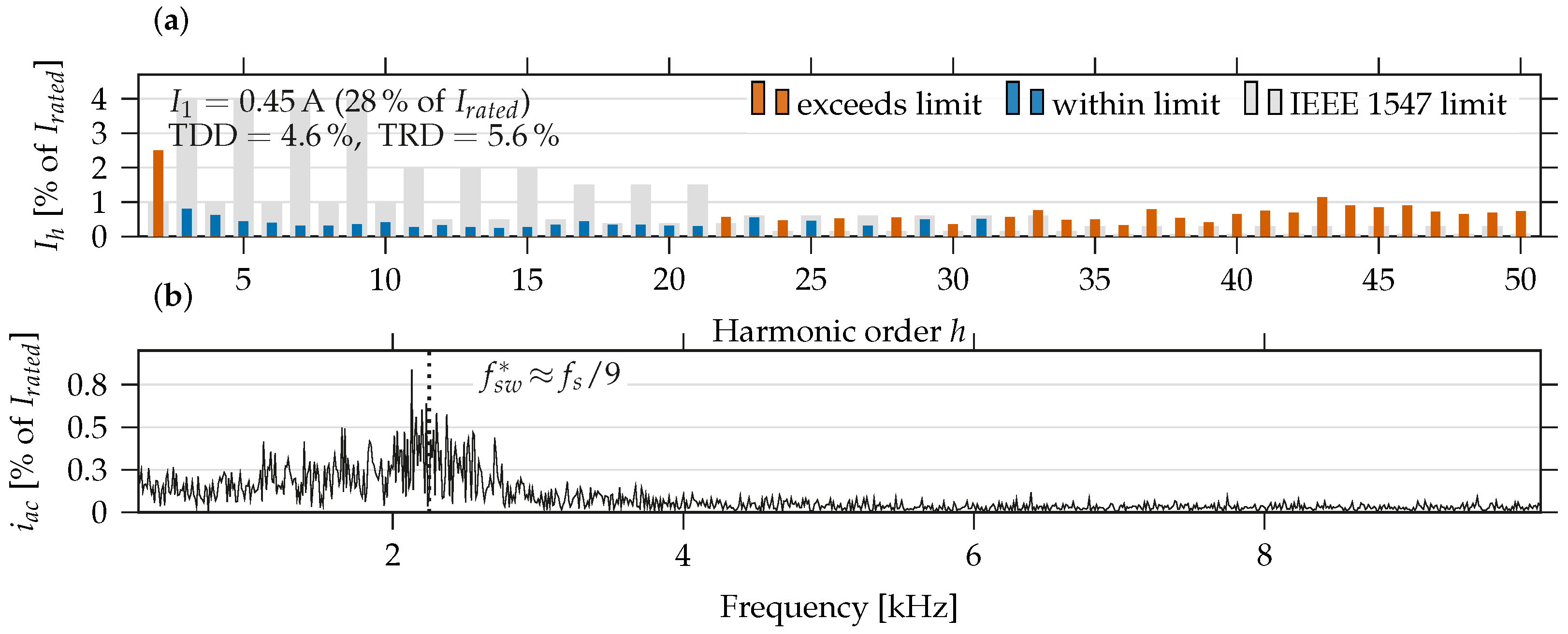
  • An experimental quantification, on the assembled prototype, of the grid-current spectrum that modulator-free predictive control produces: the dominant switching component sits at 2.25 kHz, approximately one ninth of the sampling rate, and the spread around it accounts for all but one of the 25 orders that exceed their individual IEEE 1547 limits at the higher injection level. This measures on hardware a limitation the literature reports in general terms [29]. The remaining violation, at the second harmonic, is traced to the residual dc-link ripple that the storage allocation leaves on the bus rather than to the modulation, which ties the dc-side storage split to ac-side compliance (Section 5).
  • A validation of the simulation model against the prototype in which the controller gains, the current limits, the duty clamps and the storage-split filter length are read from the firmware source, and the panel curve, the injected power and the irradiance ramp are measured, with no parameter fitted to the data. The model reproduces the 2 f a c ripple of the dc-link and its split into the UC branch to within 4.8%, and the peak and minimum dc-link voltages during an irradiance step to within 0.7% (Section 5.1).
Table 1 positions this work within representative HESS and EFL implementations. The exact linearisation of the converters’ current loops has been established for individual stages, in which the set of virtual inputs that the modulator can actually generate is rarely specified. Regarding hybrid storage, further progress has been made in [34], which discusses a battery–supercapacitor pair adapted to the Brunovsky form, where a disturbance observer absorbs the parameter uncertainty that Section 4.6 instead quantifies, and in [35], which discusses a battery-SMES pair; in both cases, the storage system is coupled to a load rather than a photovoltaic source, so neither meets the input voltage excursion that motivates the exact cancellation in this work. The prototype is derived from previous work by this group on the same converter under classical control [36,37]. What this article contributes is the internal loop law: an exact linearisation in the three dc-dc stages with the admissible set (6) expressed mathematically, along with the predictive loop of the inverter in a Texas Instruments TMS320F2837xD at 20 kHz, quantified in comparison with the single-point design it replaces (Section 4.5) and leading to a closed-form description of how the cancellation degrades under the influence of inductance and sensor error (Section 4.6).
The rest of the paper is organised as follows. Section 2 describes the system topology and its sensing; Section 3 models each subsystem and derives the EFL inner loops; Section 4 details the control strategy, from the storage current loops and the finite-set predictive inverter loop to their tuning, and contrasts the proposed control with the single-point baseline (Section 4.5); Section 5 reports the experimental validation; and Section 6 summarises the findings and outlines the remaining limitations.

2. System Description

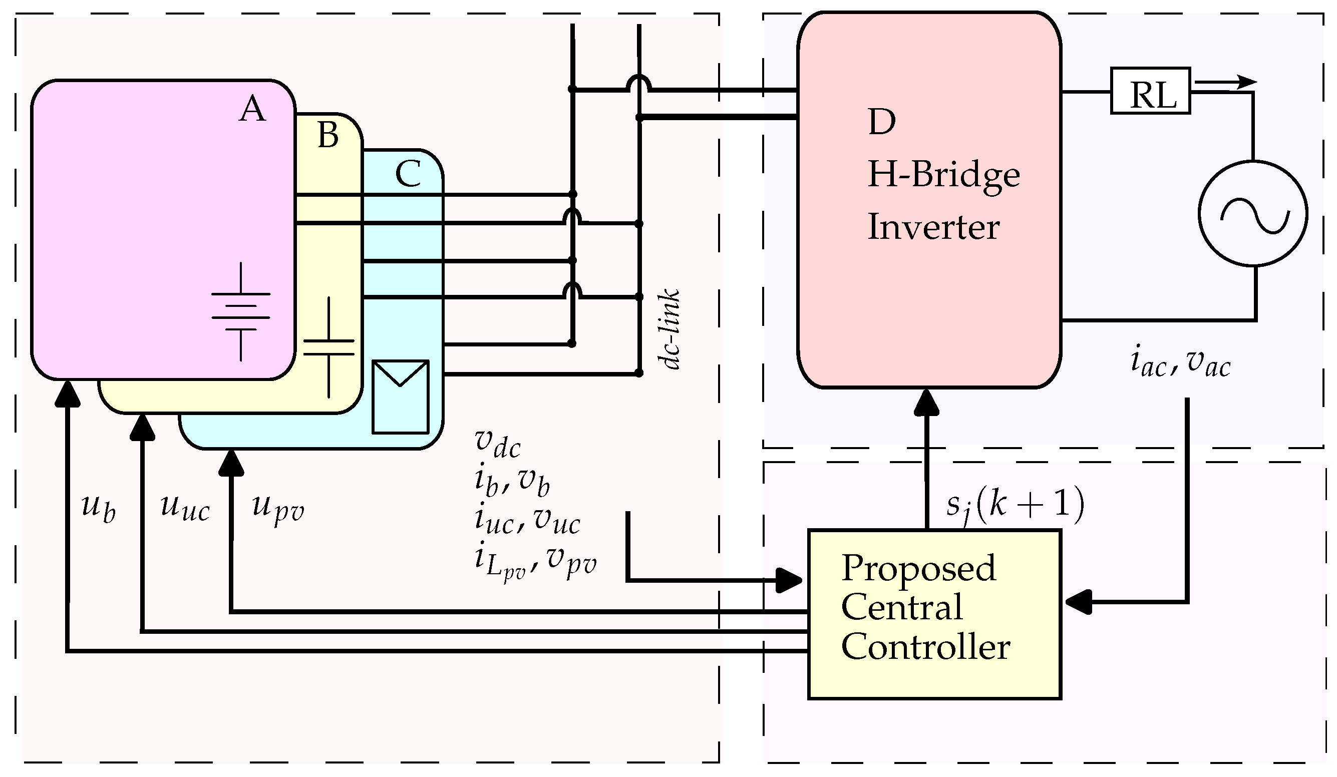
The schematic in Figure 1 illustrates the system topology. Converters A, B, and C are connected in parallel to the dc-link capacitor C d c , whereas converter D interfaces the dc-link with the ac grid. Converter A (battery bidirectional buck-boost converter—BBBC) regulates battery power flow based on PV generation and dc-link conditions. When generated power exceeds injected power, the surplus charges the battery; otherwise, the battery discharges to maintain v d c .
Converter B (UC BBBC) manages UC power, maintaining its nominal voltage and supplying peak current during fast PV transients. Converter C (PV boost converter) extracts power from the panel through a cascade whose inner current loop is exactly linearised and whose outer loop carries a fixed voltage reference 29 V. Maximum power point tracking is not implemented; the outer voltage loop holds the panel at the fixed reference 29 V and supplies the current reference the inner loop tracks. It reaches 29 V at rated irradiance and falls below it only when the boost saturates at low irradiance, as detailed in Section 5.1. Converter D (H-bridge inverter) injects power into the grid by tracking the externally provided ac current reference.
The overall system stores energy during generation hours, mitigates power peaks on the dc-link with the UC, and injects power when the battery is fully charged. These functions are coordinated by the master–slave control architecture [38], whose inner loops employ exact feedback linearisation to extend performance across wide operating ranges. The prototype instruments each converter stage with two dedicated sensors, one voltage and one current, and measures the shared dc-link voltage v d c , giving nine measurement points in total: v b and i b for converter A, v u c and i u c for converter B, v p v and i L p v for converter C, v a c and i a c for converter D, and v d c for the dc-link that couples them.

3. Proposed Solution

Each subsystem is modelled below and its EFL current loop derived.

3.1. Battery BBBC (Converter A)

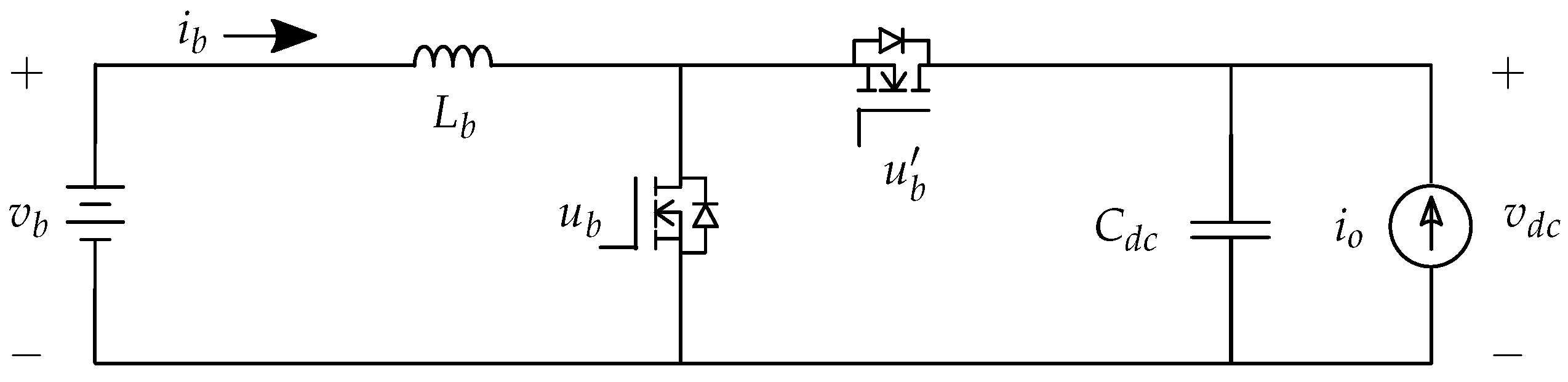
Converter A uses a BBBC to manage power flow between the battery and the dc-link (Figure 2). Its two-switch structure keeps the implementation simple and preserves bidirectional power flow capability [39].
The dynamic model is given by:
C d c d v d c d t = u b i b i o
L b d i b d t = v b v d c + u b v d c
where u b is the switch term and u b = 1 u b is the complementary switch term.
For battery charge–discharge control, a cascade control scheme is proposed, with the slave loop linearised via exact feedback linearisation. Unlike conventional linearisation methods that operate around a single equilibrium point, the proposed approach transforms the nonlinear dynamics into a linear, input-affine form that remains valid across the entire operating range, so the loop keeps its design dynamics as the operating point drifts. The transformation introduces a new control variable u b c t r l by redefining the inductor current derivative:
L b d i b d t = u b c t r l
Taking the Laplace transform of (3) with zero initial conditions defines the current-loop plant for converter A, a pure integrator:
G b c ( s ) = i b ( s ) u b c t r l ( s ) = 1 L b s
With the current dynamics linearised, the physical switching signal u b must still be derived from the virtual input u b c t r l . Substituting (3) into (2) and solving algebraically yields the modulation law:
u b = u b c t r l v b + v d c v d c
The exact linearisation transforms the nonlinear system dynamics into a linear, controllable form where u b c t r l becomes the new input variable and the actual switching signal u b is recovered from (5). The same procedure is applied to converters B and C in the following subsections. The validity of the linearisation depends on the accuracy of the measured signals v b , v u c , v p v , v d c and on knowledge of the inductances L b , L u c , L p v ; Section 4.6 quantifies both dependences: an inductance error leaves the cancellation exact and only detunes the loop, while a voltage-sensor error leaves a residual that the current loop must reject.
Two conditions delimit where (5) is defined and realisable, and both are inherited by converters B and C. First, the modulation law divides by v d c , so it is well posed only away from the origin: the dc-link must satisfy v d c v min > 0 , which the outer voltage loop enforces once the link is pre-charged. Second, the two-switch bridge only realises duty cycles in [ 0 , 1 ] . Substituting (5) into that constraint bounds the virtual input directly,
v b v d c u b c t r l v b ,
or, equivalently, a bound on the inductor-current slope that the converter can impose,
v b v d c L b d i b d t v b L b .
The interval (6) is non-empty and contains the origin, so an equilibrium exists, if and only if 0 < v b v d c , which is the step-up condition of the topology.
Whenever the outer loop requests a control action such that u b c t r l satisfies (6), the modulator remains unsaturated ( u b [ 0 , 1 ] ) and the cancellation in (3) is exact. This condition therefore defines the region where the linearising transformation is valid, although whether the closed-loop system remains inside that region depends on the evolution of v b and v d c and on the demands imposed by the outer-loop controller. Section 4.5 evaluates the closed-loop response with respect to these limits and whether the virtual input remains within the admissible interval. Analogous bounds apply to Converters B and C, replacing v b by v u c and v p v , respectively, since their modulation laws share the structure of (5).

3.2. UC BBBC (Converter B) for Fast Power Transients

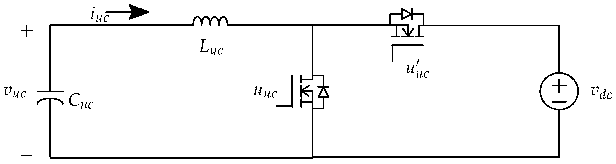
Although converter B shares the same BBBC topology as converter A (Figure 3), its control objective differs fundamentally. Whereas converter A regulates the dc-link voltage v d c while managing battery charge–discharge, converter B maintains the UC voltage v u c at its reference 24 V while absorbing and delivering high-frequency power transients that the battery cannot handle due to its slower dynamics. Both converters are implemented as physically separate power stages, each dedicated to its respective storage element.
The dynamic model for converter B mirrors converter A’s inductor dynamics, with v u c replacing v b in (2); its capacitor equation instead describes the UC node:
C u c d v u c d t = i u c
L u c d i u c d t = v u c v d c + u u c v d c
where i u c is the UC inductor current. Unlike converter A, the UC voltage dynamics (8) do not explicitly include the dc-link disturbance current i o in the control model. The UC control objective is to regulate v u c at 24 V rather than regulating v d c . The high-frequency components of the dc-link power imbalance are absorbed by the UC’s fast current response; coordination with the battery controller is achieved through the low-pass filter in the battery current reference (Section 4.2).
Applying the same exact feedback linearisation as for converter A, a virtual control input u u c c t r l is introduced by redefining the inductor current derivative:
L u c d i u c d t = u u c c t r l
Taking the Laplace transform of (10) defines the current-loop plant for converter B—again, a pure integrator:
G u c c ( s ) = i u c ( s ) u u c c t r l ( s ) = 1 L u c s
The physical switching signal for converter B is obtained by the same algebraic procedure. Substituting (10) into (9) and solving for u u c yields:
u u c = u u c c t r l v u c + v d c v d c
where u u c c t r l is the linearised control input. The key difference from converter A lies in the control objective: converter B tracks v u c rather than v d c . A moving-average filter on the battery current reference separates the frequency spectrum, allocating slow variations to the battery and fast transients to the UC; details are given in Section 4.2.

3.3. Boost Converter for PV Power Extraction

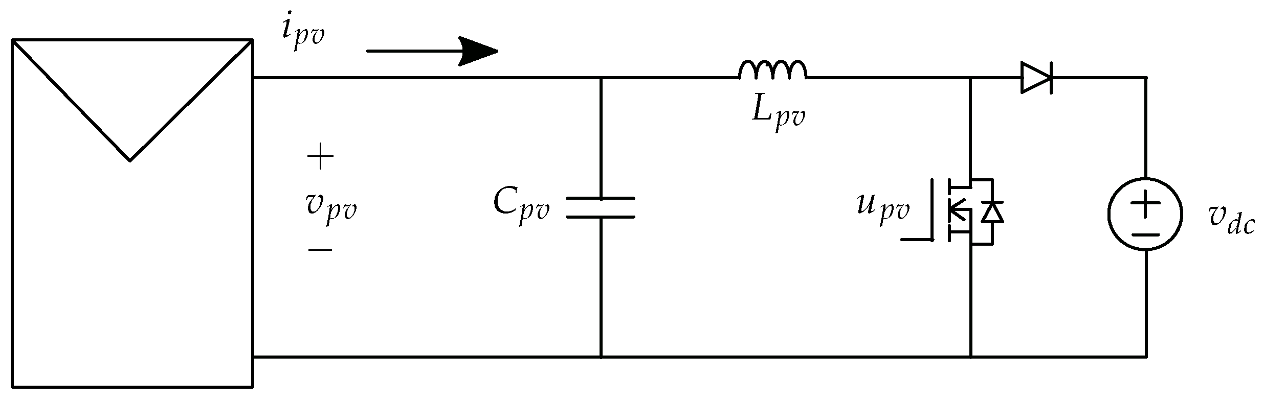
Converter C implements a unidirectional boost topology for PV power extraction, as shown in Figure 4. Its outer voltage loop carries a fixed reference 29 V, and v d c is treated as a regulated source maintained by converter A at 130 V. The dynamic model is:
C p v d v p v d t = i p v i L p v
L p v d i L p v d t = v p v v d c + u p v v d c
where u p v is the commutation term.
The current loop is linearised by the same exact feedback linearisation applied to converters A and B. Replacing the derivative term in (14) with the virtual input u p v c t r l gives:
L p v d i L p v d t = u p v c t r l
Taking the Laplace transform of (15) defines the current-loop plant for converter C, which is structurally identical to those of converters A and B:
G p v c ( s ) = i L p v ( s ) u p v c t r l ( s ) = 1 L p v s
The physical commutation term is recovered by the same procedure used for converters A and B. Substituting (15) into (14) and solving for u p v yields:
u p v = u p v c t r l v p v + v d c v d c
This modulation law (17) shares the same structural form as (5) and (12).

3.4. H-Bridge Inverter for Grid Injection

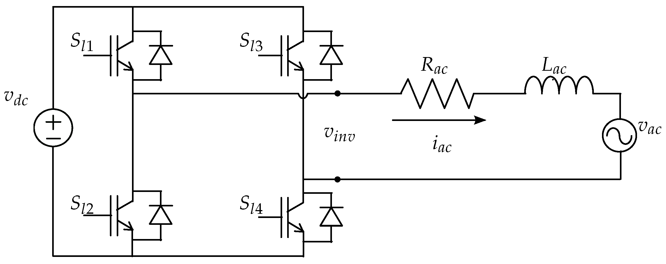
Converter D uses a full H-bridge inverter topology shown in Figure 5. For the dc-ac stage, a finite-set model predictive control (FS-MPC) strategy is employed. This approach is well-suited to the discrete nature of inverter switching states and enables direct current tracking without requiring modulation stages or cascaded control loops. At each sampling instant, the controller evaluates all valid switching states (Table 2) and selects the one that minimises a predefined cost function. Because the admissible switching states are enumerated explicitly, the converter limits are enforced by construction.
For the dc-ac stage, the topology in Figure 5 gives the following model. The inverter output voltage is:
v i n v = s j v d c
where s j is the switching function and the inverter input dc-link voltage is v d c .
In this model, the dc-link voltage v d c appearing in Equation (18) is treated as a voltage source regulated by converter A. Applying Kirchhoff’s laws, the dynamic model of the inverter is obtained.
L a c d i a c d t = i a c R a c v a c + v i n v
The continuous model (19) is the plant that the FS-MPC strategy acts upon. Its discretisation is presented in Section 4.3, where the predictive controller is developed.

4. Control Strategy

Section 4.1, Section 4.2, Section 4.3 and Section 4.4 describe the control loops and design criteria for all four converter stages, and Section 4.5 then contrasts the proposed exact-linearisation approach with a conventional single-operating-point baseline.

4.1. Description of Control Loops

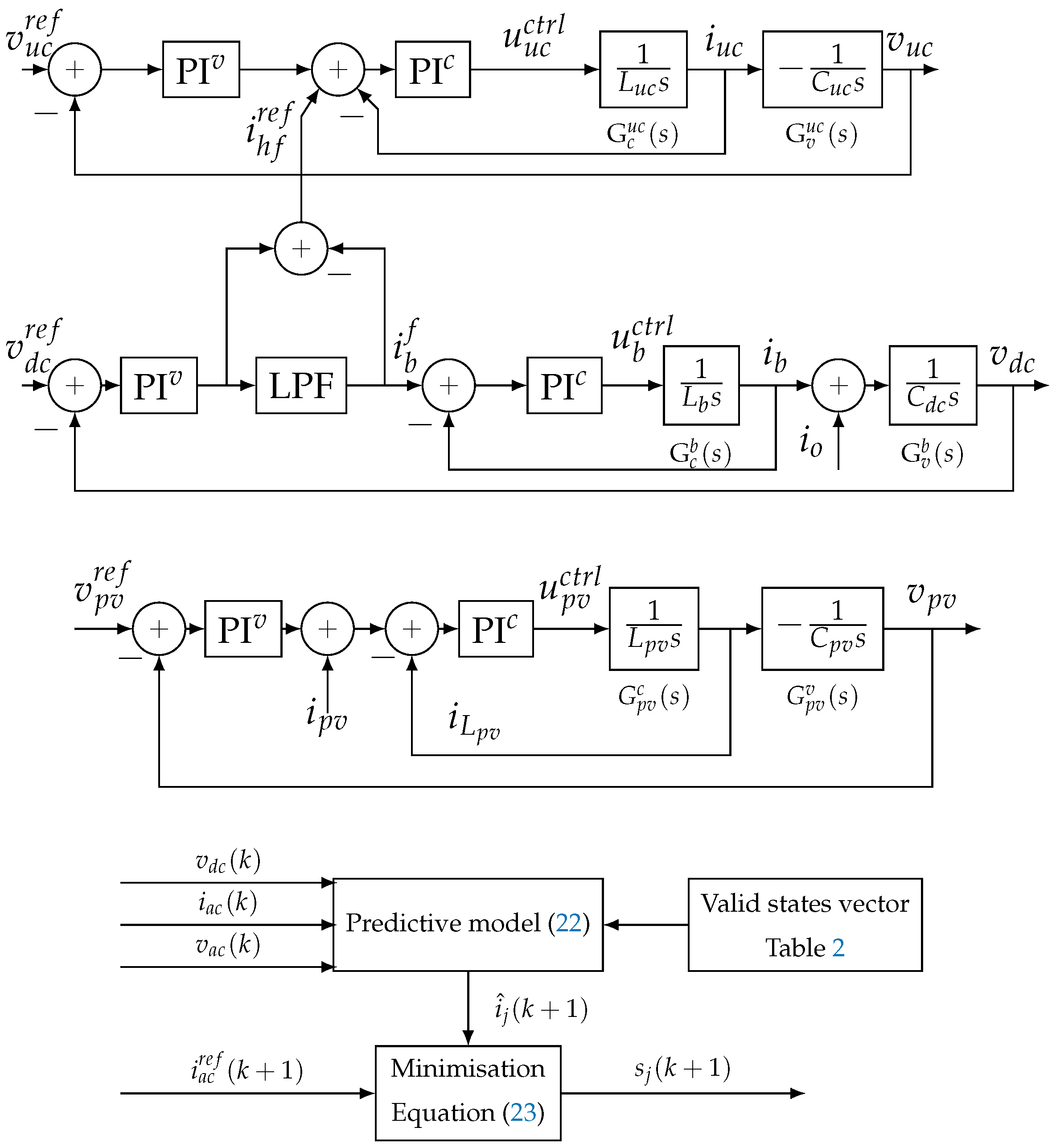
Figure 6 summarises the control loops implemented in each stage of the microinverter. Converters A–C employ a cascade (master–slave) structure with an inner current loop and an outer voltage loop, whereas converter D is controlled using FS-MPC.
In a master–slave architecture, the master loop dynamics are made slower than the slave loop dynamics, typically by a factor of five to ten, and by more where the master regulates only a slowly varying quantity such as the UC state of charge, to avoid loop interaction and preserve the time-scale separation formalised by singular-perturbation theory [40]. The sampling frequency, discretisation delays, and synchronisation between loops also constrain the achievable bandwidth [41]. Section 4.4 shows the design criteria derived from these constraints at a sampling frequency of 20 kHz.
A cascade control scheme is used for converter A. The inner current loop, implemented via EFL, is tuned at least five times faster than the outer voltage loop. Because the current loop settles long before the voltage dynamics evolve, i b i b r e f holds at the outer-loop timescale. Substituting into the dc-link balance (1) gives the outer-loop plant:
C d c d v d c d t u b i b r e f i o
where i o is the net dc-link current averaged over a switching period, comprising the inverter draw, the PV contribution and a resistive damping load connected across the link, and u b = v b / v d c is the steady-state duty complement, obtained from (2) at equilibrium. At the nominal operating point ( v b = 24 V , v d c = 130 V ), u b 0.18 . The PI voltage controller gains reported in Section 4.4 were obtained by root locus on the reduced plant (20), u b / ( C d c s ) , that is, with the duty complement retained, so that the closed loop meets the tabulated damping ratio and settling time at the nominal operating point. Because u b scales with v b / v d c , the loop becomes slower as the battery discharges and faster as v d c falls; the envelope tested in Section 5 spans this variation.
Direct closed-loop voltage regulation of the BBBC and boost converter is non-minimum-phase: both open-loop transfer functions carry a right-half-plane zero. The inductor current transfer function is free of this difficulty, so the cascade architecture closes the inner current loop first, acting on the non-minimum-phase dynamics before the outer voltage loop closes around the linearised integrating plant.

4.2. Battery and UC Control Loops

Figure 6 shows the control schemes for the two BBBC stages (converters A and B). Power is allocated between the two storage elements by frequency content. The outer dc-link voltage loop of converter A delivers the battery current reference i b r e f . In the discrete-time controller a moving average shapes this reference into a slow setpoint i b f for the battery current loop, while the complementary high-frequency part i h f r e f = i b r e f i b f is routed to the UC loop (Figure 6),
i b f ( z ) = H ( z ) i b r e f ( z ) , i h f r e f ( z ) = 1 H ( z ) i b r e f ( z ) , H ( z ) = 1 N 1 z N 1 z 1 ,
where H ( z ) is the N-sample moving average. The battery current loop then tracks i b f with the measured current as feedback, while the UC current controller tracks i h f r e f + u v u c , where u v u c is the output of the slow UC voltage loop that restores v u c to its reference. The two branches sum to unity, i b f + i h f r e f = i b r e f , so the split introduces no steady-state loss. Because the moving average shapes the reference ahead of the current loop and does not enter its feedback path, it leaves the loop’s stability unchanged. Slow demand variations (irradiance trends, load cycles) are thus handled by the battery, while fast transients are absorbed by the UC [42]. The UC controller (converter B) tracks the high-frequency components while regulating the UC voltage at v u c r e f , set by the nominal stack voltage. This frequency-based power allocation is consistent with HESS approaches for PV systems subject to rapid disturbances [22,43] and is observed in Section 5 to keep the battery current within a slow envelope while the UC absorbs the millisecond-scale transients of the tested irradiance steps.
In the prototype the split of (21) is realised as a moving average of 32 samples (Section 5.1), and its corner, at 277 Hz, is placed deliberately above the double-line frequency 2 f a c . Setting the corner at 2 f a c itself would be counterproductive for a moving average, because such a filter delays its output by half its window. A 2 f a c corner needs a window near ninety samples, whose group delay is about a fifth of the ripple period, so the high-pass residual i b r e f MA ( i b r e f ) routed to the UC would exceed the line ripple itself, its gain rising above unity. The 32-sample window used here delays by under a tenth of that period: the ripple then falls within the low-pass band and is assigned to the battery, while the UC carries the small residual measured at 0.335 A. The UC is thereby reserved for the fast irradiance transients, and the storage, rather than a bulk electrolytic dc-link capacitor, buffers the pulsating power.

4.3. Inverter Control Loop

Figure 6 shows the FS-MPC loop for converter D. To apply the predictive strategy, the continuous model (19) is discretised via a first-order Euler approximation [44,45]:
i a c ( k + 1 ) = i a c ( k ) 1 R a c T s L a c + T s L a c v i n v ( k ) v a c ( k )
The present implementation uses a one-step prediction horizon, evaluating ı ^ j ( k + 1 ) for each of the four valid switching states (Table 2) at every sampling instant k. The one-sample computational delay between measurement and actuation is not explicitly compensated in this implementation; at 20 kHz and with L a c = 70 mH, this delay introduces a phase lag below 1% of the fundamental period, negligible for fundamental tracking though it adds to the switching-band content quantified in Section 5.2. The state minimising the cost function is then applied:
J j = | i a c r e f ( k + 1 ) ı ^ j ( k + 1 ) |
where ı ^ j ( k + 1 ) is the predicted current for state j, calculated using (22). The state that produces the minimum error is applied at the next sampling instant. Because the cost depends on the switching state only through v i n v , the two zero vectors of Table 2 yield identical values of J j . The tie is resolved by alternating between them on successive occurrences, which distributes the freewheeling conduction interval between the upper and lower switch pairs and equalises their thermal loading; the choice leaves v i n v , and therefore the injected current, unchanged. This single-objective, one-step formulation prioritises current tracking and computational simplicity for real-time execution at 20 kHz. The state selected at instant k is applied at k + 1 , since the computation consumes the sampling period; the prototype does not compensate this one-step delay, and Section 5.2 shows where its cost appears. It carries a known cost. Without a modulator the switching frequency is not fixed, so the harmonic energy spreads over a band instead of clustering around a carrier, and the literature reports that this makes the individual limits of the grid codes hard to meet [29,46]. The formulation was retained here because the aim is to demonstrate that exact linearisation and predictive control can share a single processor; Section 5 measures what the choice costs in the injected current, and Section 5.1 is unaffected by it, since the storage loops act on the dc-link. Table 3 summarises the main parameters of the predictive controller.
Grid synchronisation is established without a dedicated phase-locked loop. The measured grid voltage v a c is normalised by a constant V n = 110 V , fixed at design time and not estimated on line, and the result is scaled by the injection scalar i a c r e f :
i a c r e f ( k + 1 ) = i a c r e f · v a c ( k ) V n .
This requires only the voltage sensor already used by converter D and enforces in-phase current injection by construction, provided v a c is approximately sinusoidal and the grid frequency varies slowly relative to the 20 kHz control bandwidth, conditions that held throughout the experimental tests described in Section 5.
Because V n is a constant rather than an estimate, i a c r e f is a scalar on a normalisation that assumes a grid of that amplitude, not a current command in amperes. The injected amplitude therefore tracks the grid: the peak measured across the tests was 97.09 V, so the 0.5 scalar delivered a fundamental of 0.441 A rather than 0.5 A. A grid sag scales the injected current with it. The scheme achieves its simplicity, and the absence of a second sensor, at the cost of that coupling.

4.4. Parameter Tuning

The gains of Table 4 are those the digital signal processor executed, read from the firmware source. For the dc-link loop and for the inner current loops they depart from the values a textbook design would give for the tabulated damping ratio and settling time, because those loops were retuned on the bench; the design criteria are reported alongside so that the departure is visible. Section 5.1 uses these gains, unmodified. The design parameters in Table 4 follow standard control engineering practices for cascade systems. The damping ratio ζ = 0.707 is used as a dominant-pole (root locus) tuning criterion to obtain a well-damped response, minimising oscillations while ensuring fast convergence. For the full-order closed loop, the resulting step response exhibits an overshoot of approximately 20% while meeting the targeted settling-time range. The voltage loop settling time of 10 ms is selected to be five times slower than the current loop ( 2 ms ), maintaining the master–slave hierarchy and preventing loop interaction that could lead to oscillations or instability. The sampling frequency of 20 kHz is determined by the capabilities of the digital signal processor (DSP, Texas Instruments TMS320F2837xD) and provides sufficient margin above the highest control bandwidth, ensuring adequate resolution for the predictive algorithm and pulse-width modulation (PWM) generation.
The root locus technique [47] applied to the design criteria in Table 4 sets the starting point for each loop. The current-loop design works on the linearised plants in (4), (11), and (16), which share the same integrator structure after exact feedback linearisation, so the three converters start from the same pair of gains; bench retuning then raised them to the tabulated values, a settling time of 1.11 ms at a damping ratio of 0.677 against the 2 ms and 0.707 of the design.
For the operating conditions considered in this work, practical limits reported in Table 4 are imposed by the converter topology and further reduce the achievable range. For instance, for Converter A with u max = 0.84 , the maximum attainable virtual input is + 3.2 V , corresponding to a charging-current slope of + 8.6 kA / s . Under this constraint, the considered current step requires approximately 4.6 sampling periods. Consequently, the effective operating region of the implemented controller is the clamped interval, which sets the maximum current slope that the converter can impose.

4.5. Comparison Between Proposed Control and Classical Control

The comparison is a controlled numerical study: ideal sources represent the input and dc-link voltages and only the inner current loop is closed, so the sole difference between the two controllers is the modulation law. It is run in simulation because a hardware baseline would reintroduce the measurement noise, timing and component tolerances that a clean comparison of two modulation laws must exclude, and the single-point law is a standard reference that a hardware run need not revisit. Fidelity to the hardware is established separately in Section 5. The study uses the PV boost stage, where v p v undergoes the largest deviation during the tested transients, falling from 29.1 V to about 12 V ; the conclusions transfer to converters A and B by the structural identity of their modulation laws (Section 3).
Two boost stages with identical L p v share the same ideal sources and the same PI current controller. Converter 1 applies the exact feedback linearisation of (15), computing the duty cycle from the measured voltages. Converter 2 applies the classical small-signal design: linearising (14) about the operating point ( v p v 0 , v d c 0 ) gives the equilibrium duty
u p v 0 = 1 v p v 0 v d c 0 ,
and, after discarding products of perturbations, the plant Δ i L p v / Δ u p v = v d c 0 / ( L p v s ) . The corresponding modulation law is
u p v = u p v 0 + u p v c t r l v d c 0 ,
in which both constants are frozen at the design point. Substituting (25) into (14) shows what converter 2 actually sees,
L p v d i L p v d t = v d c v d c 0 loop gain u p v c t r l + v p v v d c v p v 0 v d c 0 d .
Exact linearisation forces the loop gain to unity and d to zero identically, whatever the voltages. The classical design does neither. Two scenarios isolate the two terms. Both controllers share the same current-loop gains, k p c = 1.480 and k i c = 2959 , and the same duty limiter on [ 0 , 1 ] : what is being compared is the modulation law alone, so every other difference is removed by construction. These are the values the root locus of Section 4.4 returns for the tabulated damping ratio and settling time, not the bench-retuned gains of Table 4, because this study is a controlled comparison rather than a reproduction of the prototype.
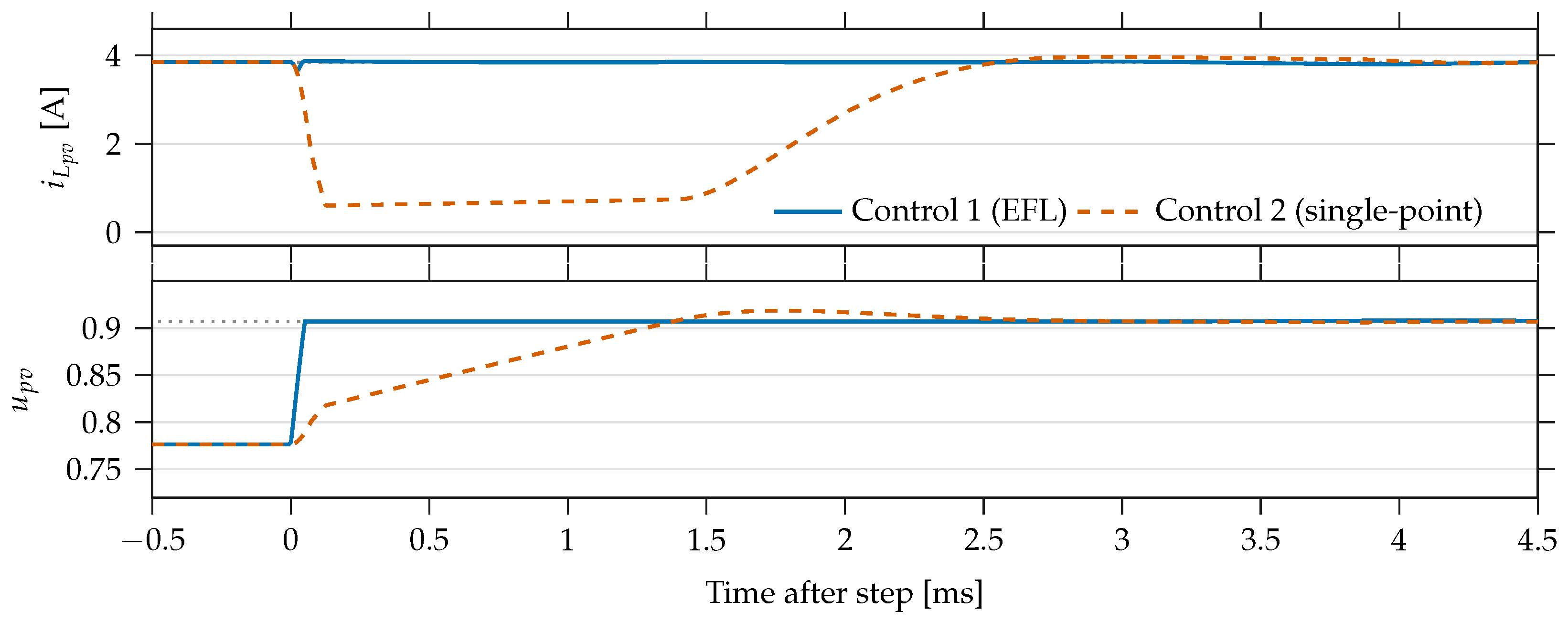
S1, input-voltage disturbance (Figure 7). With i L p v r e f held at 3.85 A and v d c at 130 V, the source steps from 29.1 V to 12.1 V , the deviation measured across the 1000 50 W / m 2 transient. This drives d = 17.0 V in (26). Exact linearisation raises the duty to its new equilibrium value of 0.907 within one switching period, a feedforward correction that cancels the disturbance before it reaches the current-loop poles, so over the 5 ms that follow the step the loop leaves a charge deficit of no more than 0.0224 A·ms, the charge it fails to inject into the dc-link over that window. The tabulated settling time those poles set is shared by both laws and is exercised by the reference step of S2, not by this disturbance rejection. The classical controller keeps applying u p v 0 = 0.776 until its integrator corrects the error: it leaves a charge deficit of 5.72 A·ms over the same window, 255 times as much, its inductor current entering discontinuous conduction for 64 μ s , and recovery takes 2.51 ms.
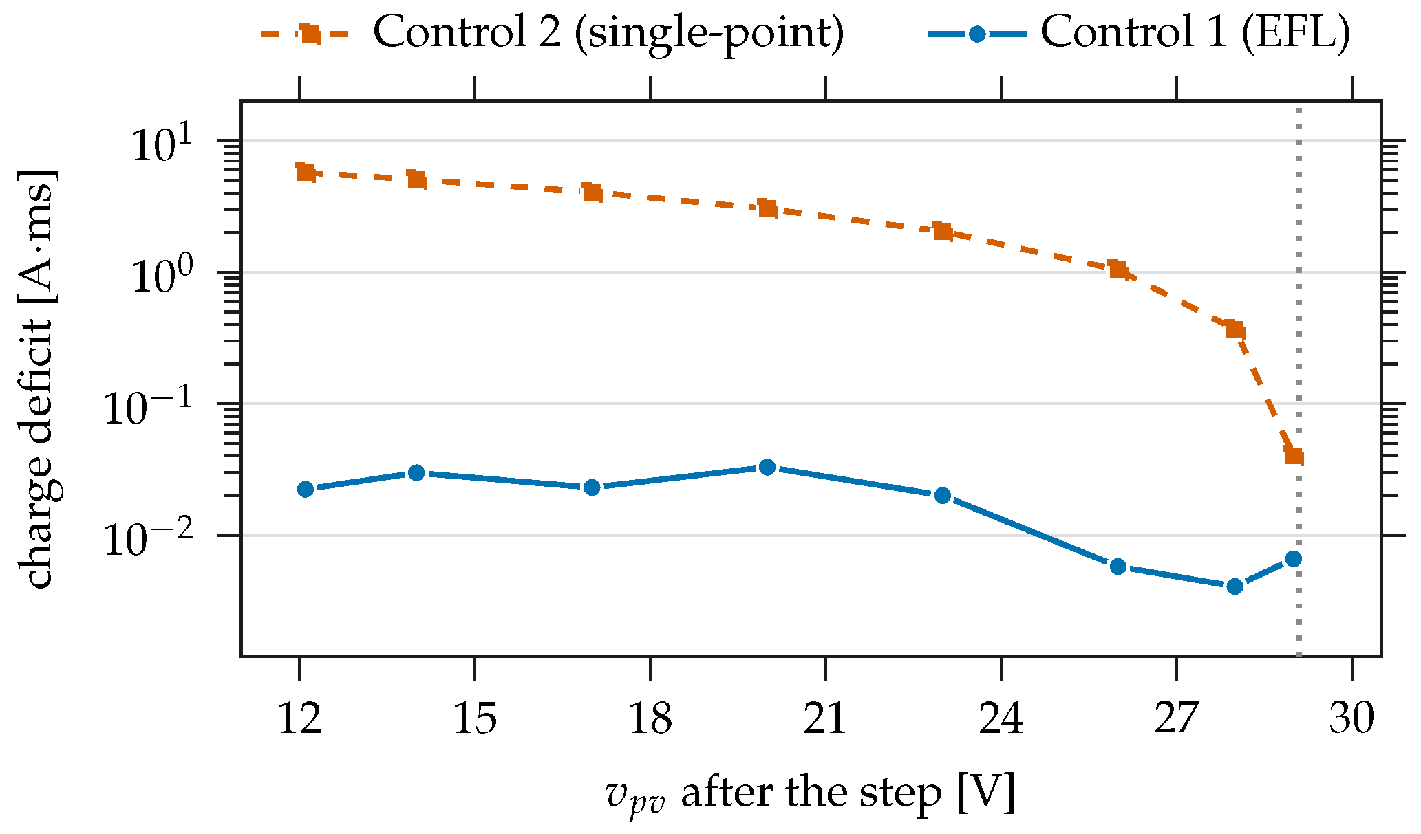
Figure 8 repeats S1 at eight input voltages, so that the comparison is a curve rather than a point. The charge deficit of the single-point design scales linearly with the disturbance, at 0.334 A · ms per volt of input-voltage drop across seven of the eight points, and its recovery time degrades in step, from 1.35 to 2.51 ms. The linearised loop stays near 0.02 A · ms throughout. The two laws converge at 29.1 V, where they are algebraically identical, which is the internal check of the sweep.
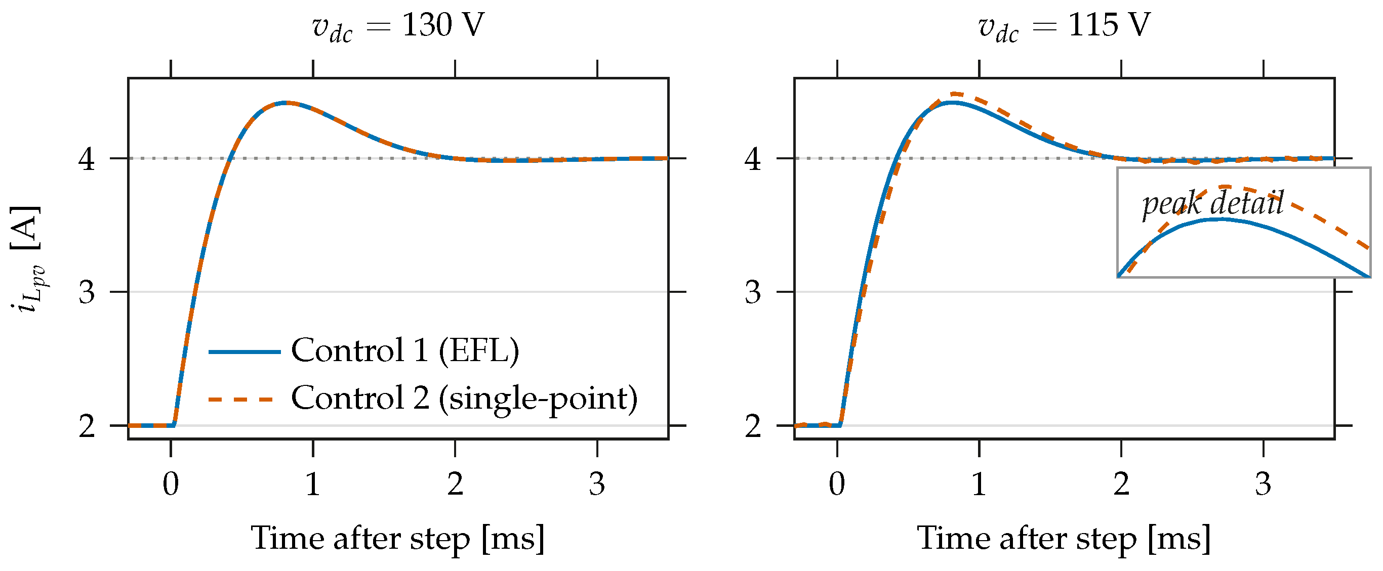
S2, dc-link deviation (Figure 9). With v p v held at 29.1 V, a 2 4 A reference step is applied at v d c = 130 V and again at 115 V , the minimum recorded during the transients. Two operating points suffice here, unlike the sweep of Figure 8, because the dc-link enters (26) only as the linear loop gain v d c / v d c 0 , so a nominal point and one off-nominal point fix the line. The input voltage, by contrast, drives the boost stage towards discontinuous conduction, so its degradation is nonlinear and needs the sweep. At the nominal bus the two laws are algebraically identical and serve as a sanity check. At 115 V the loop gain of (26) falls to 0.885 and the classical overshoot rises from 20.8 % to 24.1%, whereas exact linearisation stays at 20.9%. The degradation is real but modest, because the measured dc-link deviation reaches only about 12 % below nominal.
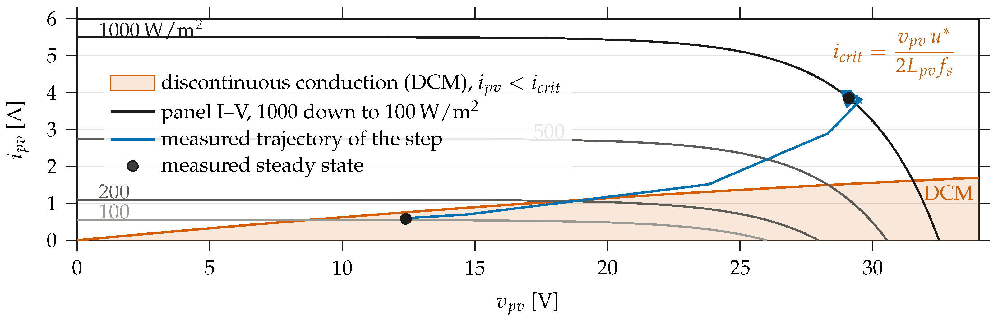
One boundary must be stated. At the low-irradiance point the equilibrium duty u * = 1 v p v / v d c =   0.905 exceeds the u max =  0.80 the firmware enforces, so the boost cannot sustain continuous conduction: the measured 0.58 A falls below the critical i c r i t = v p v u * / ( 2 L p v f s ) =  0.76 A, as Section 5.1 shows on the panel’s current–voltage plane. Both laws derive from the averaged model (13) and (14), and the cancellation that makes (15) exact is a continuous-conduction property, so neither is exact there; controllers that remain valid across the conduction-mode boundary are built on models that do not presuppose one [48] and the comparison is bounded to the continuous-conduction range. The switching model of Section 5.1 is unaffected, representing the diode directly.
Taken together (Table 5), the two scenarios locate the advantage of exact linearisation precisely. It does not lie in the dc-link deviation, where the classical design loses only three points of overshoot; it lies in the exact cancellation of the input voltage, which the classical design must reject through its integrator. The PV stage sees that disturbance as a step, and there the difference is a factor of 255 in the charge deficit it leaves and twenty-five in recovery time. Section 5 reports the exactly linearised loops on hardware; the single-point baseline was not implemented, so this comparison is numerical only.
On the S1 and S2 steps the demanded duty stays within the admissible set (6), so the advantage of exact linearisation holds throughout the realisable range; outside that set the modulator saturates and, by construction, no modulation law can track the reference.

4.6. Parameter Sensitivity

The linearisation of feedback in hybrid storage systems has previously been evaluated under uncertain parameters for a combination of a battery and superconducting magnetic energy storage in a simulation [35]. For the law in (17), each uncertainty can be expressed in closed form. Writing the measured voltages as v p v ( 1 + ε p v ) and v d c ( 1 + ε d c ) , with ε p v and ε d c the relative gain errors of the two sensors, and substituting (17) into (14) gives
L p v d i L p v d t = u p v c t r l 1 + ε d c + v p v 1 1 + ε p v 1 + ε d c d ,
which has the structure of (26), consisting of a loop gain and a residual, and reduces to (15) when both errors vanish.
Inductance does not appear in (17), so it does not appear in (27) either: an inductance error results in d 0 , and the cancellation is exact, regardless of the mismatch. It acts solely on the loop designed on (16), whose poles satisfy L p v s 2 + k p c s + k i c = 0 , so that both are divided by 1 + δ when the actual inductance is L p v ( 1 + δ ) , δ being its relative mismatch. The square root roughly halves the effect: an error of ± 20 % , twice the tolerance specified in Section 3, shifts the damping ratio from 0.707 to a value between 0.646 and 0.791, and does not affect the modulation law.
An error in the voltage sensor does reach the cancellation. At ± 2 % on both sensors, in the combination of signs that yields the largest value of d, the residual reaches 0.49 V at the final point of 12.1 V for S1, compared to the 17.0 V left at the same point by the fixed duty cycle of the single-point design, a factor of 34; the loop gain deviates from unity by a maximum of 2%. The two residuals also move in opposite directions as the input voltage drops: (27) is proportional to v p v and therefore decreases from 1.19 V at the design point to 0.49 V, while that of (26) grows from zero to 17.0 V.
Noise in the current measurement does not affect (17), which uses only the two voltages. It reaches the duty cycle through u p v c t r l alone, and is therefore attenuated by the current loop, just as it would be with any other modulation law.

5. Experimental Results

The irradiance transitions tested in this work, including steps from 1000 W / m 2 to 50 W / m 2 , from 1000 W / m 2 to 200 W / m 2 , and from 100 W / m 2 to 1000 W / m 2 , replicate conditions reported in real-world scenarios such as pavement photovoltaics under vehicle shadows, where power drops can exceed 60% of the rated power for intervals of 0.05 to 0.2 s [43]. Such extreme transients challenge the HESS and control architecture more severely than gradual cloud-induced variations, making them suitable benchmarks for demonstrating the robustness of the proposed control strategy under worst-case operating conditions.
The dc-link capacitance is 9.6 µ F in total, distributed as 400 V film capacitors across the stages that share the bus: 2.2 µ F at the output of each bidirectional converter and 5.2 µ F at the input of the H-bridge. The PV boost has no output capacitor. Its role is local high-frequency decoupling at the shared dc-link, rather than bulk energy storage. Low-frequency energy buffering and dc-link voltage regulation are provided by the actively controlled battery–UC HESS; under the tested conditions, this arrangement maintained v d c at 130 V.
The main parameters used for this experiment are shown in Table 6. The complete real-time control system, including the dc-dc stages (converters A, B, and C) and the dc-ac stage (converter D), was implemented and executed in a single DSP at a sampling frequency of 20 kHz.
Under these conditions, the behaviour of the state variables is evaluated, including the UC current ( i u c ), PV current ( i p v ), battery current ( i b ), ac current ( i a c ), dc-link voltage ( v d c ), UC voltage ( v u c ), PV voltage ( v p v ), and ac voltage ( v a c ).
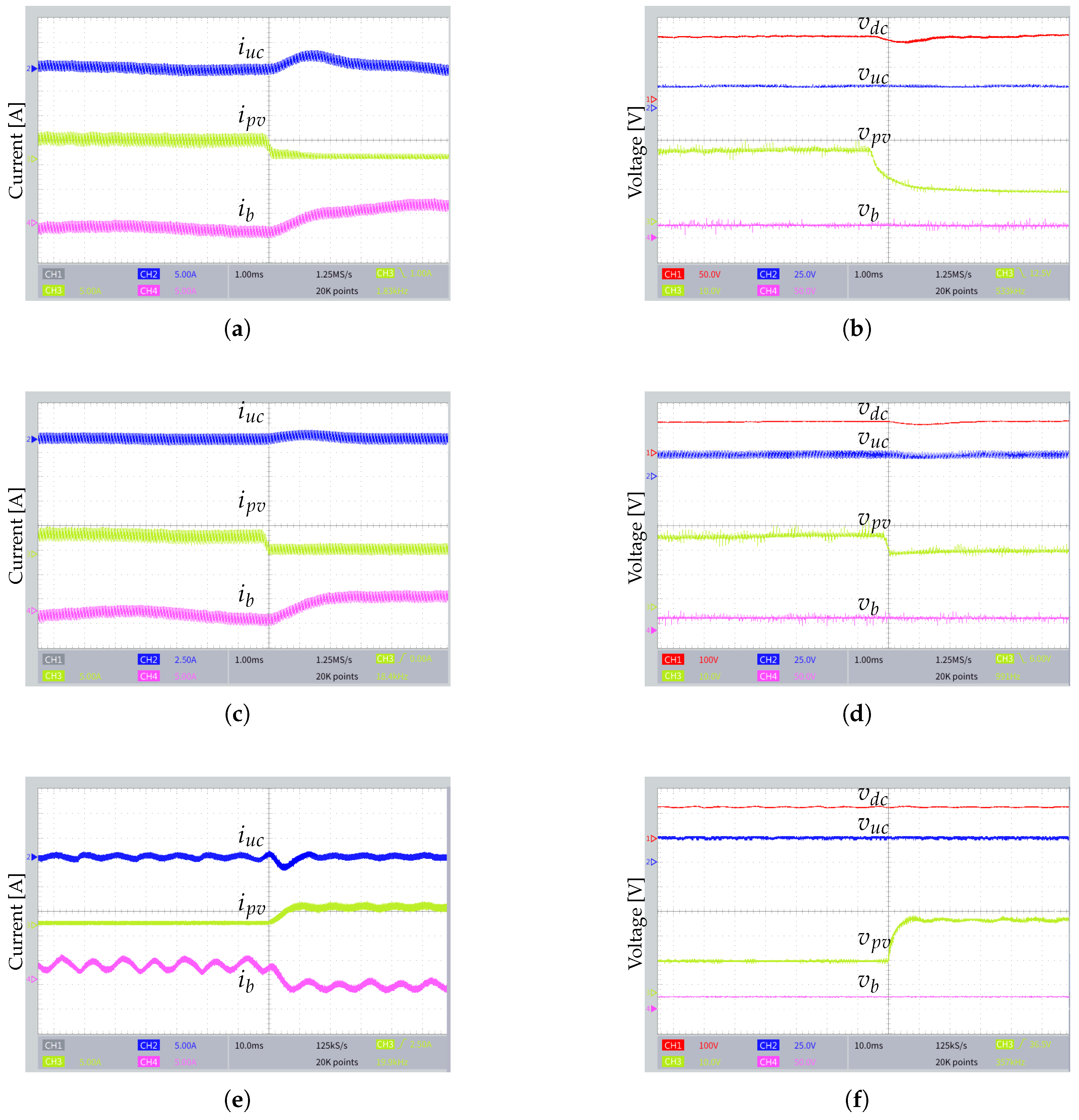
Figure 10a,b show that during the initial 75 ms the PV system operates at an irradiance of 1000 W / m 2 , with v p v = 29.1 V and i p v = 3.85 A, that is, 112 W delivered by the EA PSI 9000 running the EN 50530 profile at 25   ° C ; these three quantities are read from the source front panel rather than from the oscilloscope traces. The surplus power above the grid injection target would drive v d c upward; converter A responds by commanding a negative i b , transferring excess energy to the battery. Consequently, v d c is held at 130 V while the battery charges.
After 75 ms, the irradiance decreases from 1000 W / m 2 to 50 W / m 2 , with v p v = 12.1 V. For this transient, the direction of i b reverses due to the dc-link power deficit; therefore, the controller commands power delivery from the battery to the dc-link to restore v d c to its 130 V reference. As designed in Section 4.2, the UC responds with a transient current peak of 2.8 A in its switching-period average, rising from a pre-step level of 0.28 A; the instantaneous peak measured is 3.9 A, once the 2.26 A peak-to-peak switching ripple is included to absorb the fast disturbance components while maintaining v u c at 24 V, whereas the battery handles the slower power rebalancing. As a result, v d c remains regulated despite the large decrease in PV generation.
Figure 10c,d illustrates the system response to an irradiance change from 1000 W / m 2 to 200 W / m 2 . The general behaviour is similar to that shown in Figure 10a,b; however, after 75 ms, the irradiance change is smaller, which implies that the current delivered by the battery to the dc-link is smaller to restore the power balance. With the higher PV power available, both the battery current magnitude and the UC peak current are lower than in the 95% drop scenario.
Figure 10e,f shows the system initially operating with an irradiance of 100 W / m 2 , with v p v = 12.4 V and i p v = 0.58 A. At this irradiance the duty cycle saturates at the u max = 0.80 enforced by the firmware, the stage enters discontinuous conduction, and the operating point settles where the converter characteristic meets the panel I–V curve, delivering 7 W (Figure 11). It is not set by the voltage reference. For t < 75 ms, the reduced PV generation prompts the battery control system to inject current into the dc-link, maintaining v d c at its reference. For t > 75 ms, as PV generation returns to rated irradiance ( 1000 W / m 2 ), i b transitions from positive to negative, indicating power absorption by the battery. This change is smoothly managed by the UC control, which absorbs the high-frequency components of the power change.
The single-phase grid connection introduces a second-harmonic ripple at twice the grid frequency in the dc-side signals; Figure 10e,f shows a time window long enough to observe this component.
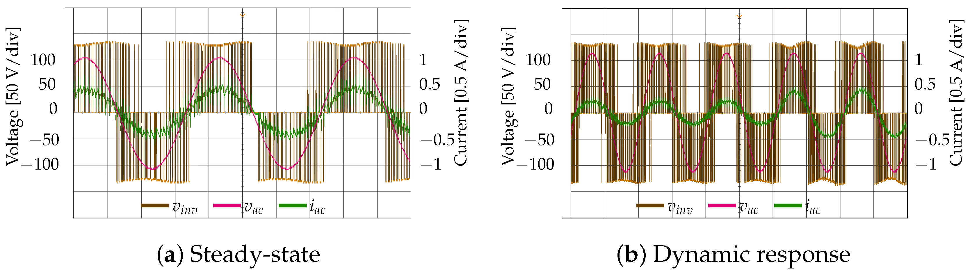
Figure 12a shows the dc-ac stage of the microinverter. The ac current i a c is in phase with the grid voltage v a c , and the switched inverter voltage v i n v has amplitude 130 V and is updated at the sampling frequency 20 kHz. Both v a c and i a c retain their amplitudes during the irradiance transients, indicating that the dc-side transients do not reach the ac amplitudes. The coupling that does remain is spectral: the residual 2 f a c ripple of the bus reappears as a second harmonic of the injected current, and Section 5.2 quantifies it.
In Figure 12b, the injected current follows a reference step from 0.5 A to 1 A at 60 ms, reaching the new level while staying in phase with v a c . The harmonic content of that current is examined in Section 5.2, where the spectrum turns out to be the limiting factor rather than the tracking.

5.1. Model Validation

The simulation model is validated against the experimental prototype under the irradiance rise from 100 W / m 2 to 1000 W / m 2 of Figure 10e,f. Three quantities are taken from that test: the UC current, the dc-link voltage, and the photovoltaic current. The grid voltage and current come from a separate steady-state ac capture at the same injection reference and enter only the firmware-based check at the end of this section.
The PI controller gains are specified in Table 4, together with their current limits and duty clamps. Windup is handled by limiting the integral accumulator state, which is preserved between sampling instants and would otherwise continue to grow while the modulator remains saturated. The limit is ± 0.1 in the current loops of converters A and B and ± 0.01 in both loops of converter C. This mechanism is particularly relevant in the photovoltaic stage because, at 100 W / m 2 , the duty cycle approaches u max = 0.80 , so the voltage-loop accumulator would otherwise continue integrating an error that the saturated converter cannot correct. With this limit in place, the operating point stabilises where the saturated converter characteristic intersects the panel’s I–V curve (Figure 11), which is the behaviour described below.
The high- and low-frequency split between the battery and UC current references is performed by a moving-average filter of 32 samples applied to the battery current reference i b r e f , whose 3 dB corner falls at 277 Hz; the low-frequency output feeds the battery loop and the high-frequency complement is routed to the UC, as in (21). The dc-link capacitance is 9.6 µF of film capacitors. The filter length is taken from the firmware, not fitted to the data: 32 samples is the value the prototype’s split filter uses, so the measured division of the 2 f a c ripple between the two branches, the corresponding row of Table 7, is an independent test on the same footing as the dc-link, photovoltaic and ac-side rows. The simulated panel has an open-circuit voltage of 32.5 V and a short-circuit current of 5.5 A, and a 8.4 ms irradiance ramp reproduces the emulator’s rise. The simulation is resampled onto the oscilloscope’s 8 µ s grid before any quantity is read (see the Table 7 caption).
Every figure quoted below comes from Table 7 and validates the model against the measurements. In steady state at 100 W / m 2 , the 2 f a c component of v d c agrees to 3.3%, that of i u c to 4.8%, and the phase error between the two is only 5.4°, which shows that the split of the pulsating power between the two storage elements is reproduced in magnitude as well as in phase. The agreement is reinforced by the mean dc-link voltage, 130.35 V simulated against 130.28 V measured, and by the photovoltaic current, matched to within 9.9% at rated irradiance and 5.2% at low irradiance. Finally, the duty cycle the firmware would command at rated irradiance, 0.788, agrees with the 0.776 that the measured terminal voltage implies, which confirms the fidelity of the model in steady state.
The low-irradiance terminal voltage also agrees, 11.7 V simulated against 12.4 V measured (6%), so the steady operating points are reproduced at both irradiance levels. The model departs from the prototype only in the transient, where the dc-link deviation is overestimated by 27% and the UC peak current by 69%, and in the switching ripple of i u c , overestimated by 63%. All three are overestimates of transient magnitudes, whereas each steady-state entry in Table 7 agrees with an accuracy of 9.9%. The measurement bandwidth does not explain them, since the simulation is decimated to the oscilloscope’s 8 µs grid before any quantities are evaluated, so both undergo the same sampling. Nor does the uncertainty in the component values explain them, which would spread the errors in both directions rather than in just one. The remaining explanation is the damping absent from the model, namely the parasitic series resistance of the UC branch and the finite switching transitions that the averaged model idealises.
The outer voltage loop of the photovoltaic stage regulates the panel terminal voltage to its fixed reference 29 V, and its output is the current reference the exactly linearised inner loop tracks. At rated irradiance the measured terminal voltage is 29.1 V against the 29 V setpoint, so the loop holds its reference. At 100 W / m 2 it instead sits at 12.4 V, on the panel’s current-source branch: at that irradiance the stage runs in discontinuous conduction with its duty against the firmware clamp, so the operating point is set by where the saturated converter characteristic meets the panel I–V curve (Figure 11), not by the reference. No maximum-power-point tracking is attempted: with the fixed reference the prototype extracts 87% of the available power at rated irradiance and 74% at 100 W / m 2 , which bound what a maximum-power-point algorithm on top of the exactly linearised inner loop would recover, while the inner loop tracks correctly throughout.
The check that follows uses no dc-link quantity, so it is independent of the storage-ripple agreement established above. Taken from the code, the predictive controller normalises the measured grid voltage by the design constant V n = 110 V of (24) and scales it by 0.5. With that scalar and the measured peak 97.09 V, the reference amplitude is fixed at 0.441 A without touching any measured current or dc-link quantity, and contrasted against the measured fundamental of i a c , 0.431 A: a difference of 2.3%. That agreement settles the injection scalar actually running (a value of 1.0 would give 0.88 A and disagree), the normalisation constant, and the predictive controller’s tracking error, which the remaining 2.3% measures. The same capture gives a 3 phase between v a c and i a c , a power factor of 0.999, an injected power of 20.9 W against 21.0 W measured, and a pulsating-power balance of 0.173 A (battery and UC 2 f a c phasors referred to the bus) against the 0.159 A the inverter draws.
The switching model was built in PSIM Professional 2026 and the firmware compiled in Code Composer Studio 12.3.0 for the Texas Instruments TMS320F2837xD.

5.2. Harmonic Analysis

The harmonic spectrum of the injected grid current i a c was measured at two injection levels, one low and one high. Writing I 1 for the rms value of its fundamental, these are I 1 =  0.29 A and I 1 =  0.45 A, or 18% and 28% of the rated current I r a t e d =  1.63 A rms. Figure 13 plots the higher of the two, which is the worst case. Both spectra come from a coherent transform over an integer number of grid cycles, so no window function or leakage correction is needed. Repeated captures reproduce the total rated distortion (TRD) to within 0.4 percentage points.
Figure 13a refers each harmonic to the rated current, the base that IEEE 1547 uses, with the limit of each order drawn behind it in grey. Interharmonic content is grouped into the nearest integer order as an equivalent rms value, following IEC 61000-4-7 and the treatment of [29]; without this step more than half of the distortion would escape the count. At the operating point plotted, 25 orders exceed their individual limits. The even orders, whose limit IEEE 1547 sets at a quarter of the 0.3 % odd-order value, begin to fail from the 22nd; from the thirty-third upward every order fails, even and odd alike: the 44th and 46th reach 0.9 % of rated current against a 0.075 % limit, twelve times over, and that band is where the switching energy of the predictive control lands.
One violation, however, sits at the other end of the spectrum, and it is not a property of the modulation. The second harmonic reaches 2.49% of rated current against a 1.0 % limit. Its origin is the dc-link: the 2 f a c ripple of v d c , which the hybrid storage does not fully absorb, modulates the output of the H-bridge, whose terminal voltage is the bus voltage multiplied by the switching state, and reappears as an even harmonic in the injected current. It grows with the injected current, from 0.2 % at the lower operating point, where it complies, to 2.49% at the higher one, where it does not. The residual ripple that the storage allocation leaves on the bus therefore has a cost on the grid side.
Figure 13b explains why, and it does so in frequency rather than harmonic order, because the distortion of a finite-set controller is not concentrated on discrete harmonics. Lacking a modulator, the controller holds a switching state for as long as it remains optimal, so its switching frequency is neither fixed nor equal to the sampling rate, and the harmonic energy spreads over a broad band rather than clustering around a carrier [29,46]. The spectrum is therefore shown raw, without smoothing: the spread is the result. The dominant switching component sits at f s w * = 2.25 kHz, close to f s / 9, an integer fraction of the sampling frequency [46]. This is not the average switching frequency, which counts device transitions and gives 5.2 kHz here [49], more than twice f s w * . The band around f s w * maps onto harmonic orders 40 to 50, where IEEE 1547 tightens its individual limits to 0.3 % of rated current.
Two distortion figures summarise the spectrum, defined in (28), and answer different questions:
TDD = h = 2 50 I h 2 I r a t e d , TRD = I r m s 2 I 1 2 I r a t e d ,
where I h is the rms value of the h-th harmonic and I r m s that of the whole current. The total demand distortion (TDD) counts integer harmonics only; the TRD of IEEE 1547-2018 counts interharmonics and noise as well. The measured values are 3.5% and 4.6% for the former, and 3.8% and 5.6% for the latter, against a 5 % limit that the total rated distortion exceeds at the higher injection.
Both kinds of limit, the individual and the aggregate, must be read together: a converter can sit below the aggregate limit and still breach the standard by exceeding its individual limits, all the more at high order, where they are stricter. The 25 orders that fail contribute only 4.1 % in quadrature, which fits inside the 5 % envelope. The standard is written that way on purpose, to stop energy being deposited at any single frequency however small the total, and that is exactly what a modulator-free predictive controller does: little distortion, spread across the band where the limits are tightest. This prototype therefore fails the individual limits at both operating points, 25 orders at the higher and 24 from order 18 upward at the lower, and the aggregate only at the higher. At the lower point, where the aggregate is met with a rated distortion of 3.8%, the non-compliance is one of shape, not size.
Distortion grows with injected current rather than staying flat, because the switching frequency is unbounded by construction and the output stage is a single 70 mH inductor, with no LCL section to attenuate what lands at 2.25 kHz. The remedies are known and none was implemented: delay compensation, a modulated scheme that restores a fixed switching frequency [50], and an LCL stage each attenuate the ripple, whereas a switching-effort penalty [51] lowers the frequency by weighting device transitions against tracking error in the cost function.
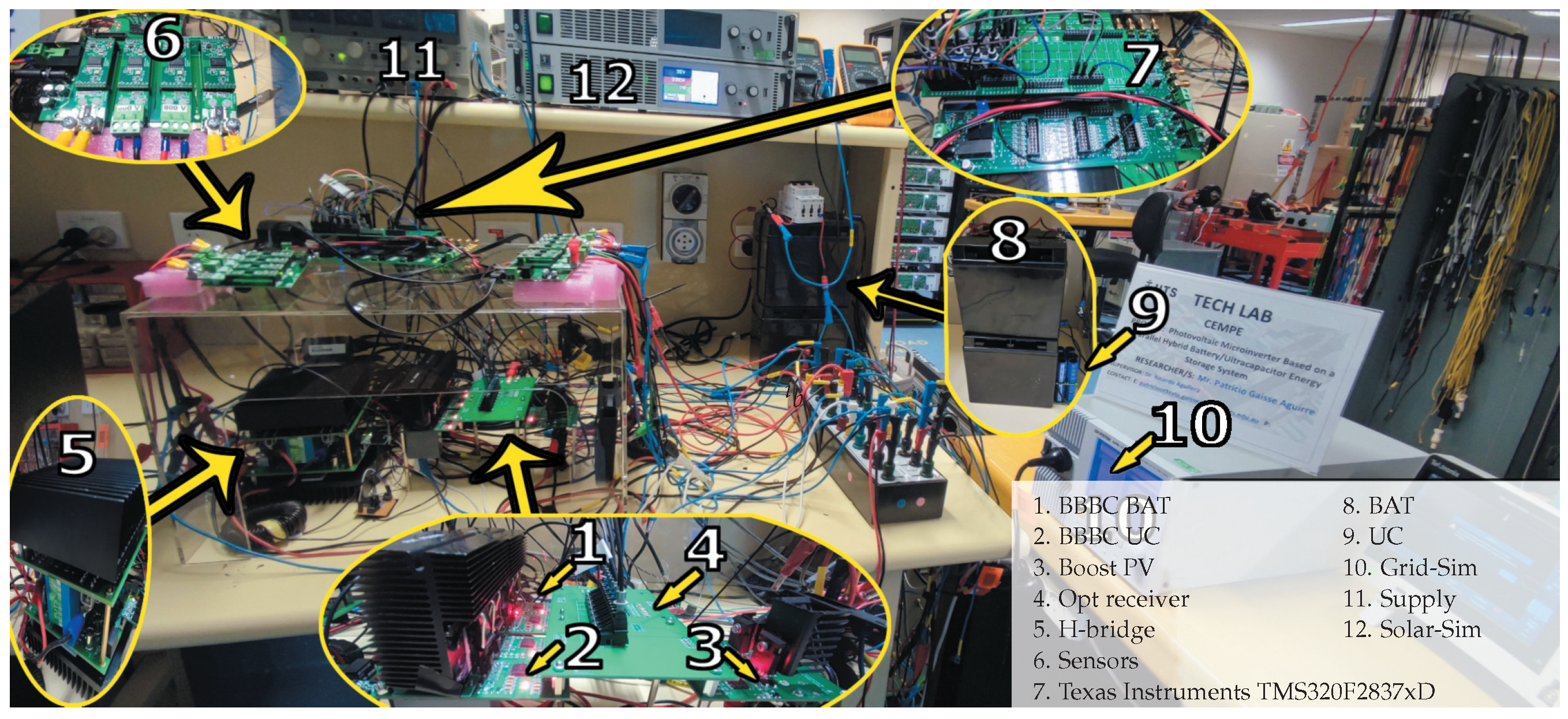
Finally, Figure 14 shows the experimental prototype with each of its components indicated.

6. Conclusions

A PV microinverter prototype with a battery–UC HESS in active parallel arrangement was implemented and tested under three severe irradiance step profiles ( 1000 50 , 1000 200 , and 100 1000 W / m 2 ). The master–slave control based on exact feedback linearisation regulated the dc-link voltage at its 130 V setpoint across the transients, its peak-to-peak deviation below 16% during the most severe step, the 1000 50 W / m 2 profile of Figure 10, with the UC supplying transient current peaks of 2.8 A to protect the battery from millisecond-scale disturbances under the prototype’s constant-parameter model. The simulation comparison against a single-point linearisation baseline (Section 4.5) confirmed that EFL holds its nominal overshoot and settling time ( t s = 2 ms , ζ = 0.707 ) as the dc-link voltage departs from the design point and cancels the input-voltage disturbance that a single-point design can only reject through its integrator—properties that conventional small-signal methods lose outside their linearisation neighbourhood. All three converter types ran simultaneously on a single Texas Instruments TMS320F2837xD at 20 kHz, so combined EFL and FS-MPC is computationally feasible on this class of microinverter platform.
With no modulator or LCL stage, the prototype does not meet the IEEE 1547 individual harmonic limits (Section 5.2); this is a property of the output stage, not of the control demonstrated here. As built, the unit serves primarily as a platform for validating the proposed control strategy, whereas achieving the power quality required for grid connection would require additional output-stage conditioning through filtering, modulation, or a combination of both. The AC output remained stable during the reference step from 0.5 A to 1 A. The switching model was validated against the prototype based on the firmware gains and the measured boundary conditions, without adjusting any parameters to the data (Section 5.1): It reproduces the ripple of the dc-link and its distribution to the UC with an accuracy of 4.8%, the maximum and minimum bus voltages with an accuracy of 0.7%, and the amplitude of the injected current, based solely on the grid voltage, with an accuracy of 2.3%. The agreement is not uniform, as the model overestimates the transient deviation of the dc-link by 27%, the maximum current of the UC by 69%, and its switching ripple by 63%, so it serves as a reliable guide for steady-state operating points and the extremes of the dc-link, and a conservative guide for transient peaks. These results are valid for the single-phase topology. Furthermore, they hold only under continuous conduction, since at one-tenth of the irradiance the boost stage crosses into discontinuous conduction (Section 5.1), and the cancellation that (17) provides is a continuous-conduction property.
Several aspects remain open. Multi-objective FS-MPC that bounds the average switching frequency and delay-compensated variants would help meet the individual IEEE 1547 limits the modulator-free controller misses, and a three-phase extension would remove the second-harmonic contribution to them; hardware-in-the-loop testing is a natural next step. The exactly linearised PV loop is built to track a maximum-power-point-tracking reference, which the fixed-reference prototype does not yet supply: it extracts 87% and 74% of the available power at rated and one-tenth irradiance, which such an algorithm would raise. A tertiary supervisory controller could set the grid-injection reference from the available PV power and the battery state of charge, closing the energy-management loop the external reference leaves open. On-line estimation of the inductances and battery state of charge would carry EFL beyond its constant-parameter assumption. End-to-end efficiency and power factor beyond the single point measured (0.999) are a priority for the follow-on campaign.


Author Contributions

Conceptualization, P.G. and J.M.; methodology, P.G., J.M. and R.A.; software, P.G.; formal analysis, P.G., D.R. and R.A.; investigation, P.G.; resources, J.M., M.R. and C.R.; writing—original draft, P.G.; writing—review and editing, J.M., D.R., R.A., M.R. and C.R.; supervision, J.M.; funding acquisition, J.M., M.R. and C.R. All authors have read and agreed to the published version of the manuscript.

Funding

This research was funded by the Agencia Nacional de Investigación y Desarrollo under projects: ANID/FONDECYT/1231015, ANID Becas/Doctorado Nacional 21200824 and ANID/SERC-Chile/CIN250043. The authors also appreciate the support provided by the Engineering Systems Doctoral Program, Faculty of Engineering, University of Talca; the Research Project PINV01-272 of the National Council of Science and Technology (CONACYT); A7C200 IRCF Project from the University of Nottingham; the Programa de Redução de Assimetrias na Pós-Graduação (PRAPG)—Edital nº 14/2023-DRI-CAPES. ID Number: 046.821.818-15; FONDECYT Iniciación Project no. 11261540 and 24EVDT-262305 CORFO Project.

Data Availability Statement

The original contributions presented in this study are included in the article. Further inquiries can be directed to the corresponding author.

Acknowledgments

The authors would like to extend their gratitude to the School of Electrical and Data Engineering, University of Technology Sydney.

Conflicts of Interest

The authors declare no conflicts of interest.

Abbreviations

The following abbreviations are used in this manuscript:
BBBCBidirectional buck-boost converter
DSPDigital signal processor
EFLExact feedback linearisation
FS-MPCFinite-set model predictive control
HESSHybrid energy storage system
LCLInductor–capacitor–inductor
MPCModel predictive control
PIProportional-integral
PVPhotovoltaic
PWMPulse-width modulation
SMESSuperconducting magnetic energy storage
TDDTotal demand distortion
TRDTotal rated distortion
UCUltracapacitor

References

  1. Haegel, N.M.; Verlinden, P.; Victoria, M.; Altermatt, P.; Atwater, H.; Barnes, T.; Breyer, C.; Case, C.; De Wolf, S.; Deline, C.; et al. Photovoltaics at multi-terawatt scale: Waiting is not an option. Science 2023, 380, 39–42. [Google Scholar] [CrossRef] [Scilit] [PubMed]
  2. Jäger-Waldau, A. Snapshot of Photovoltaics – February 2024. EPJ Photovolt. 2024, 15, 21. [Google Scholar] [CrossRef] [Scilit] [PubMed]
  3. REN21. Renewables 2025 Global Status Report; Technical Report; Renewable Energy Policy Network for the 21st Century (REN21): Paris, France, 2025. [Google Scholar]
  4. Romero-Cadaval, E.; Spagnuolo, G.; Franquelo, L.G.; Ramos-Paja, C.A.; Suntio, T.; Xiao, W.M. Grid-Connected Photovoltaic Generation Plants: Components and Operation. IEEE Ind. Electron. Mag. 2013, 7, 6–20. [Google Scholar] [CrossRef] [Scilit]
  5. Kouro, S.; Leon, J.I.; Vinnikov, D.; Franquelo, L.G. Grid-Connected Photovoltaic Systems: An Overview of Recent Research and Emerging PV Converter Technology. IEEE Ind. Electron. Mag. 2015, 9, 47–61. [Google Scholar] [CrossRef] [Scilit]
  6. Celik, O.; Teke, A.; Tan, A. Overview of micro-inverters as a challenging technology in photovoltaic applications. Renew. Sustain. Energy Rev. 2018, 82, 3191–3206. [Google Scholar] [CrossRef] [Scilit]
  7. Alluhaybi, K.; Batarseh, I.; Hu, H. Comprehensive Review and Comparison of Single-Phase Grid-Tied Photovoltaic Microinverters. IEEE J. Emerg. Sel. Top. Power Electron. 2020, 8, 1310–1329. [Google Scholar] [CrossRef] [Scilit]
  8. Ikkurti, H.P.; Saha, S. A comprehensive techno-economic review of microinverters for Building Integrated Photovoltaics (BIPV). Renew. Sustain. Energy Rev. 2015, 47, 997–1006. [Google Scholar] [CrossRef] [Scilit]
  9. Hasan, R.; Mekhilef, S.; Seyedmahmoudian, M.; Horan, B. Grid-connected isolated PV microinverters: A review. Renew. Sustain. Energy Rev. 2017, 67, 1065 1080. [Google Scholar] [CrossRef] [Scilit]
  10. Chen, B.; Gu, B.; Zhang, L.; Zahid, Z.U.; Lai, J.S.; Liao, Z.; Hao, R. A High-Efficiency MOSFET Transformerless Inverter for Nonisolated Microinverter Applications. IEEE Trans. Power Electron. 2015, 30, 3610–3622. [Google Scholar] [CrossRef] [Scilit]
  11. Huang, Q.; Huang, A.Q.; Yu, R.; Liu, P.; Yu, W. High-Efficiency and High-Density Single-Phase Dual-Mode Cascaded Buck Boost Multilevel Transformerless PV Inverter With GaN AC Switches. IEEE Trans. Power Electron. 2019, 34, 7474–7488. [Google Scholar] [CrossRef] [Scilit]
  12. Rahimi, R.; Farhangi, S.; Farhangi, B.; Moradi, G.R.; Afshari, E.; Blaabjerg, F. H8 Inverter to Reduce Leakage Current in Transformerless Three-Phase Grid-Connected Photovoltaic systems. IEEE J. Emerg. Sel. Top. Power Electron. 2018, 6, 910–918. [Google Scholar] [CrossRef] [Scilit]
  13. Li, Q.; Yang, Y.; Yu, X.; Li, H. A 700 W·h·kg−1 Rechargeable Pouch Type Lithium Battery. Chin. Phys. Lett. 2023, 40, 048201. [Google Scholar] [CrossRef] [Scilit]
  14. Wasim, M.S.; Habib, S.; Amjad, M.; Bhatti, A.R.; Ahmed, E.M.; Qureshi, M.A. Battery-Ultracapacitor Hybrid Energy Storage System to Increase Battery Life Under Pulse Loads. IEEE Access 2022, 10, 62173–62182. [Google Scholar] [CrossRef] [Scilit]
  15. Momayyezan, M.; Abeywardana, D.B.W.; Hredzak, B.; Agelidis, V.G. Integrated Reconfigurable Configuration for Battery/Ultracapacitor Hybrid Energy Storage Systems. IEEE Trans. Energy Convers. 2016, 31, 1583–1590. [Google Scholar] [CrossRef] [Scilit]
  16. Czagány, M.; Hompoth, S.; Keshri, A.K.; Pandit, N.; Galambos, I.; Gácsi, Z.; Baumli, P. Supercapacitors: An Efficient Way for Energy Storage Application. Materials 2024, 17, 702. [Google Scholar] [CrossRef] [Scilit] [PubMed]
  17. Saeed, M.; Briz, F.; Guerrero, J.M.; Larrazabal, I.; Ortega, D.; Lopez, V.; Valera, J.J. Onboard Energy Storage Systems for Railway: Present and Trends. IEEE Open J. Ind. Appl. 2023, 4, 238–259. [Google Scholar] [CrossRef] [Scilit]
  18. Kurm, S.; Agarwal, V. Hybrid Energy Storage System Based on a Novel Reduced Rating Multi-Input Converter. IEEE Trans. Power Electron. 2020, 35, 12133–12142. [Google Scholar] [CrossRef] [Scilit]
  19. Hajiaghasi, S.; Salemnia, A.; Hamzeh, M. Hybrid energy storage system for microgrids applications: A review. J. Energy Storage 2019, 21, 543–570. [Google Scholar] [CrossRef] [Scilit]
  20. Adeyinka, A.M.; Esan, O.C.; Ijaola, A.O.; Farayibi, P.K. Advancements in hybrid energy storage systems for enhancing renewable energy-to-grid integration. Sustain. Energy Res. 2024, 11, 26. [Google Scholar] [CrossRef] [Scilit]
  21. Chemali, E.; Preindl, M.; Malysz, P.; Emadi, A. Electrochemical and Electrostatic Energy Storage and Management Systems for Electric Drive Vehicles: State-of-the-Art Review and Future Trends. IEEE J. Emerg. Sel. Top. Power Electron. 2016, 4, 1117–1134. [Google Scholar] [CrossRef] [Scilit]
  22. Kotra, S.; Mishra, M.K. A Supervisory Power Management System for a Hybrid Microgrid With HESS. IEEE Trans. Ind. Electron. 2017, 64, 3640–3649. [Google Scholar] [CrossRef] [Scilit]
  23. Meshram, V.S.; Corti, F.; Lozito, G.M.; Costanzo, L.; Reatti, A.; Vitelli, M. Small-Signal Modeling, Comparative Analysis, and Gain-Scheduled Control of DC–DC Converters in Photovoltaic Applications. Electronics 2025, 14, 4308. [Google Scholar] [CrossRef] [Scilit]
  24. Sira-Ramírez, H.; Ilic-Spong, M. Exact linearization in switched-mode DC-to-DC power converters. Int. J. Control 1989, 50, 511–524. [Google Scholar] [CrossRef] [Scilit]
  25. Judewicz, M.G.; González, S.A.; Gelos, E.M.; Fischer, J.R.; Carrica, D.O. Exact Feedback Linearization Control of Three-Level Boost Converters. IEEE Trans. Ind. Electron. 2023, 70, 1916–1926. [Google Scholar] [CrossRef] [Scilit]
  26. Sun, J.; Xia, J.; Ding, S.; Yu, X. Exact-Feedback-Linearization-Based Adaptive Second-Order Sliding Mode Control Design for DC–DC Boost Converters. IEEE Trans. Ind. Electron. 2025, 72, 5397–5407. [Google Scholar] [CrossRef] [Scilit]
  27. Sun, Y.; Zhu, J.; Fu, C.; Chen, Z. Decoupling Control of Cascaded Power Electronic Transformer Based on Feedback Exact Linearization. IEEE J. Emerg. Sel. Top. Power Electron. 2022, 10, 3662–3676. [Google Scholar] [CrossRef] [Scilit]
  28. Vazquez, S.; Rodriguez, J.; Rivera, M.; Franquelo, L.G.; Norambuena, M. Model Predictive Control for Power Converters and Drives: Advances and Trends. IEEE Trans. Ind. Electron. 2017, 64, 935–947. [Google Scholar] [CrossRef] [Scilit]
  29. Karamanakos, P.; Liegmann, E.; Geyer, T.; Kennel, R. Model Predictive Control of Power Electronic Systems: Methods, Results, and Challenges. IEEE Open J. Ind. Appl. 2020, 1, 95–114. [Google Scholar] [CrossRef] [Scilit]
  30. Nam, N.N.; Nguyen, N.D.; Yoon, C.; Lee, Y.I. Disturbance Observer-Based Robust Model Predictive Control for a Voltage Sensorless Grid-Connected Inverter with an LCL Filter. IEEE Access 2021, 9, 109793–109805. [Google Scholar] [CrossRef] [Scilit]
  31. Nam, N.N.; Nguyen, N.D.; Yoon, C.; Choi, M.; Lee, Y.I. Voltage Sensorless Model Predictive Control for a Grid-Connected Inverter with LCL Filter. IEEE Trans. Ind. Electron. 2022, 69, 740–751. [Google Scholar] [CrossRef] [Scilit]
  32. Xue, C.; Zhou, D.; Li, Y. Hybrid Model Predictive Current and Voltage Control for LCL-Filtered Grid-Connected Inverter. IEEE J. Emerg. Sel. Top. Power Electron. 2021, 9, 5747–5760. [Google Scholar] [CrossRef] [Scilit]
  33. Zamani, H.; Abbaszadeh, K.; Karimi, M.H.; Gyselinck, J. Adaptive Model Predictive Control for LCL-Filter Grid-Tied Inverters. IEEE Trans. Ind. Electron. 2023, 71, 2818–2828. [Google Scholar] [CrossRef] [Scilit]
  34. Song, G.; Liu, X.; Xiao, G.; Chen, B.; Wang, P. Decentralized Adaptive Control Strategy of DC–DC Boost Converter for Hybrid Energy Storage Systems Feeding CPLs. IEEE J. Emerg. Sel. Top. Power Electron. 2024, 12, 3663–3674. [Google Scholar] [CrossRef] [Scilit]
  35. Tang, C.; Huang, Y. Feedback Linearization Control Design for Battery/SMES Hybrid Energy Storage Systems Used in Distribution Network. Front. Energy Res. 2021, 9, 751884. [Google Scholar] [CrossRef] [Scilit]
  36. Venegas, L.; Muñoz, J.; Tapia, O. Power Sharing Strategy for PV Microinverter with Embedded Hybrid Energy Storage System. In Proceedings of the 2022 International Symposium on Power Electronics, Electrical Drives, Automation and Motion (SPEEDAM), Sorrento, Italy, 22–24 June 2022; pp. 889–895. [Google Scholar] [CrossRef] [Scilit]
  37. Tapia, O.; Muñoz, J.; Venegas, L. Control Strategy for a Three-Phase Microinverter with an Embedded Hybrid Energy Storage System. In Proceedings of the 2022 IEEE International Conference on Environment and Electrical Engineering and 2022 IEEE Industrial and Commercial Power Systems Europe (EEEIC/I&CPS Europe), Prague, Czech Republic, 28 June–1 July 2022; pp. 1–7. [Google Scholar] [CrossRef] [Scilit]
  38. Du, Z.; Yufan, F.; Yang, X.; Li, J. Design of PI Controller for a Class of Discrete Cascade Control Systems. IEEE Trans. Autom. Sci. Eng. 2023, 20, 2607–2615. [Google Scholar] [CrossRef] [Scilit]
  39. Gorji, S.A.; Sahebi, H.G.; Ektesabi, M.; Rad, A.B. Topologies and Control Schemes of Bidirectional DC–DC Power Converters: An Overview. IEEE Access 2019, 7, 117997–118019. [Google Scholar] [CrossRef] [Scilit]
  40. Khalil, H.K. Nonlinear Systems, 3rd ed.; Prentice Hall: Upper Saddle River, NJ, USA, 2002. [Google Scholar]
  41. Pirsto, V.; Kukkola, J.; Hinkkanen, M. Multifunctional Cascade Control of Voltage-Source Converters Equipped With an LC Filter. IEEE Trans. Ind. Electron. 2022, 69, 2610–2620. [Google Scholar] [CrossRef] [Scilit]
  42. Roy, P.; He, J.; Liao, Y. Cost Minimization of Battery-Supercapacitor Hybrid Energy Storage for Hourly Dispatching Wind-Solar Hybrid Power System. IEEE Access 2020, 8, 210099–210115. [Google Scholar] [CrossRef] [Scilit]
  43. Mao, M.; Tang, Y.; Ma, F.; Sun, H.; Hua, G.; Li, P. A Three-Level Hierarchical Power Smoothing Control Strategy for Pavement Photovoltaics Under Vehicle Shadow Disturbance. IEEE Trans. Power Electron. 2026, 41, 1053–1065. [Google Scholar] [CrossRef] [Scilit]
  44. Park, D.H.; Tahir, H.; Lee, J.D.; Kim, R.Y. Hierarchical Single-Objective Model Predictive Control With Reduced Computational Burden in Cascaded H-Bridge Converter Based on 3-Level Flying Capacitor Unit Cell. IEEE Access 2022, 10, 54730–54741. [Google Scholar] [CrossRef] [Scilit]
  45. Aguilera, R.P.; Acuna, P.; Yu, Y.; Konstantinou, G.; Townsend, C.D.; Wu, B.; Agelidis, V.G. Predictive Control of Cascaded H-Bridge Converters Under Unbalanced Power Generation. IEEE Trans. Ind. Electron. 2017, 64, 4–13. [Google Scholar] [CrossRef] [Scilit]
  46. Tricarico, T.; Costa, J.A.; Herrera, D.; Galván-Díez, E.; Carrasco, J.M.; Aredes, M. Total Frequency Spread: A New Metric to Assess the Switching Frequency Spread of FCS-MPC. Energies 2022, 15, 5273. [Google Scholar] [CrossRef] [Scilit]
  47. Freijedo, F.D.; Vidal, A.; Yepes, A.G.; Guerrero, J.M.; Lopez, O.; Malvar, J.; Doval-Gandoy, J. Tuning of Synchronous-Frame PI Current Controllers in Grid-Connected Converters Operating at a Low Sampling Rate by MIMO Root Locus. IEEE Trans. Ind. Electron. 2015, 62, 5006–5017. [Google Scholar] [CrossRef] [Scilit]
  48. Parada Salado, J.G.; Herrera Ramírez, C.A.; Soriano Sánchez, A.G.; Rodríguez Licea, M.A. Nonlinear Stabilization Controller for the Boost Converter with a Constant Power Load in Both Continuous and Discontinuous Conduction Modes. Micromachines 2021, 12, 522. [Google Scholar] [CrossRef] [Scilit] [PubMed]
  49. Karamanakos, P.; Geyer, T. Guidelines for the Design of Finite Control Set Model Predictive Controllers. IEEE Trans. Power Electron. 2020, 35, 7434–7450. [Google Scholar] [CrossRef] [Scilit]
  50. Tarisciotti, L.; Zanchetta, P.; Watson, A.; Bifaretti, S.; Clare, J.C. Modulated Model Predictive Control for a Seven-Level Cascaded H-Bridge Back-to-Back Converter. IEEE Trans. Ind. Electron. 2014, 61, 5375–5383. [Google Scholar] [CrossRef] [Scilit]
  51. Vargas, R.; Cortes, P.; Ammann, U.; Rodriguez, J.; Pontt, J. Predictive Control of a Three-Phase Neutral-Point-Clamped Inverter. IEEE Trans. Ind. Electron. 2007, 54, 2697–2705. [Google Scholar] [CrossRef] [Scilit]
Figure 1. Proposed microinverter scheme: converters A (battery BBBC), B (ultracapacitor BBBC) and C (PV boost) in active parallel on the shared dc-link, converter D (H-bridge inverter) injecting into the grid through an RL filter, all coordinated by the central controller.
Mathematics 14 03269 g001
Figure 2. BBBC topology for battery (Converter A). The current source i o is the net current drawn by the other converters connected in parallel at the dc-link.
Mathematics 14 03269 g002
Figure 3. BBBC topology for UC (Converter B). This stage regulates the UC voltage v u c and handles high-frequency power transients.
Mathematics 14 03269 g003
Figure 4. Boost converter for PV power extraction.
Mathematics 14 03269 g004
Figure 5. Full H-bridge topology of converter D, switching the dc-link voltage into the R a c L a c filter for grid-current injection.
Mathematics 14 03269 g005
Figure 6. Control schemes for all converter stages: battery/UC bidirectional converters (A and B), PV boost (C), and H-bridge inverter (D).
Mathematics 14 03269 g006
Figure 7. S1, input-voltage disturbance. The source steps from 29.1 V to 12.1 V at t = 0 with i L p v r e f held at 3.85 A and v d c = 130 V . Exact linearisation (solid) reaches the new equilibrium duty within one switching period; the single-point design (dashed) holds the stale duty until its integrator corrects it. Currents and duty cycles are averaged over one switching period for display.
Mathematics 14 03269 g007
Figure 8. S1 across the operating range: charge deficit over the 5 ms that follow the step, against the input voltage reached after it, one curve per control law. The dotted line marks the design point 29.1 V, where the two laws are algebraically identical. Same metric as Table 5.
Mathematics 14 03269 g008
Figure 9. S2, dc-link deviation. Reference step 2 4 A with v p v = 29.1 V . At the nominal bus the two laws are algebraically identical. At 115 V the loop gain of the single-point design falls to 0.885 and its overshoot rises from 20.8 % to 24.1%, while exact linearisation is unchanged. The inset magnifies the peak.
Mathematics 14 03269 g009
Figure 10. Experimental dc-side waveforms, one irradiance step profile per row: left, inductor currents i u c , i p v , i b ; right, dc voltages v d c , v u c , v p v , v b . (a) DC-side currents during a 95% irradiance drop ( 1000 50 W / m 2 ) (time base: 1.00 ms/div). (b) DC-side voltages during a 95% irradiance drop ( 1000 50 W / m 2 ) (time base: 1.00 ms/div). (c) DC-side currents during an 80% irradiance drop ( 1000 200 W / m 2 ) (time base: 1.00 ms/div). (d) DC-side voltages during an 80% irradiance drop ( 1000 200 W / m 2 ) (time base: 1.00 ms/div). (e) DC-side currents during a tenfold irradiance rise ( 100 1000 W / m 2 ) (time base: 10.0 ms/div). (f) DC-side voltages during a tenfold irradiance rise ( 100 1000 W / m 2 ) (time base: 10.0 ms/div).
Mathematics 14 03269 g010
Figure 11. Conduction mode of the PV boost stage on the panel’s current–voltage plane. Shaded: discontinuous conduction. Panel curves span 1000 to 100 W / m 2 ; the line is the measured 100 1000 W / m 2 trajectory, extracted from the oscilloscope captures, and the markers its two steady states.
Mathematics 14 03269 g011
Figure 12. Experimental ac-side waveforms: (a) steady-state v i n v , v a c , and i a c at nominal injection; (b) dynamic response to a current-reference step from 0.5 A to 1 A at 60 ms.
Mathematics 14 03269 g012
Figure 13. Spectrum of the injected grid current at the higher operating point tested ( I 1 = 0.45 A rms, 28% of rated). (a) Individual harmonics against their own IEEE 1547 limits (grey bars); the fundamental is omitted. (b) The same record in frequency, shown raw without smoothing. Coherent transform over five grid cycles at 20 kHz.
Mathematics 14 03269 g013
Figure 14. Experimental prototype.
Mathematics 14 03269 g014
Table 1. Representative experimentally validated HESS and exact-feedback-linearisation implementations, positioned against this work by storage, control law, and application scope.
Ref.Storagedc–dc ControlShared dc-Link 1PV + Grid
[22]BAT+UCSupervisory PI
[18]BAT+UCCurrent-mode, MIC××
[25]NoneEFL, three-level boost××
[27]NoneEFL decoupling, MIMO×
[26]NoneEFL, sliding mode××
[34]BAT+UCEFL, Brunovsky form×
[36,37]BAT+UCPower sharing, PI
This workBAT+UCEFL cascade
1 Two or more converter stages sharing a single dc-link. Abbreviations: BAT, battery; UC, ultracapacitor (termed supercapacitor in the cited works); EFL, exact feedback linearisation; MIC, multi-input converter; MIMO, multi-input multi-output; PV, photovoltaic.
Table 2. The dc-ac converter valid states.
v i n v S l 1 S l 2 S l 3 S l 4
00101
01010
+ v d c 1001
v d c 0110
Table 3. Model predictive control parameters.
ParameterValue
Sampling period ( T s ) 50 µ s (20 kHz)
Prediction horizon1 step
Valid states4 (Table 2)
Weighting factorsSingle objective
Cost functionEquation (23)
Table 4. Design criteria and controller gains for converters A, B, and C 1.
Design criteria
Converter t s v ζ v t s c ζ c
A 10 ms 0.707 2 ms 0.707
B 4 s 0.707 2 ms 0.707
C 10 ms 0.707 2 ms 0.707
Controller gains
Converter k p v k i v k p c k i c
A 0.050756 198.7 2.6751 10,540
B 0.800875 0.2957 2.6751 10,540
C 0.2437 104.2 2.6751 10,540
Reference and Modulation Limits
Converter i min r e f i max r e f u min u max
A 15  A + 15  A0.010.84
B 2  A + 2  A0.000.84
C 100  A + 100  A00.80
1  t s v , ζ v : voltage loop settling time and damping ratio; t s c , ζ c : current loop settling time and damping ratio; k p v , k i v : voltage loop proportional and integral gains; k p c , k i c : current loop proportional and integral gains; i min r e f , i max r e f : limits applied to the current reference output by the voltage loop; u min , u max : limits on the modulator’s duty cycle. The six values are read from the firmware source code. The limit for converter C is wide enough that it is never triggered: at the rated power 112 W the reference remains below 4 A, so the duty cycle limit u max = 0.80 is what limits that stage.
Table 5. Controlled comparison between Control 1 (exact feedback linearisation) and Control 2 (single-point linearisation) on the PV boost inner current loop. Ideal sources; identical PI gains; duty limited to [ 0 , 1 ] .
ScenarioMetricControl 1 (EFL)Control 2 (Single-Point)
S1: input-voltage step, v p v : 29.1 12.1  VCharge deficit over 5 ms 1≤0.0224 A·ms5.72 A·ms
Discontinuous conductionnone 64 μ s
Recovery to ± 0.05  A < 0.1  ms2.51 ms
S2: reference step 2 4  A, v d c = 130  VOvershoot20.8%20.8%
Settling time (2%)1.75 ms1.76 ms
S2: reference step 2 4  A, v d c = 115  VOvershoot20.9%24.1%
Settling time (2%)1.76 ms1.79 ms
1  ( i L p v i L p v r e f ) d t over the 5 ms that follow the step, evaluated on the unaveraged current: the switching ripple has zero mean and cancels in the integral, so the figure needs no smoothing parameter.
Table 6. Prototype parameters.
System Parameters
L b 0.37 mH C u c 10 F
C d c 9.6 µ F v d c 130 V
C p v 10 µ F f a c 50 Hz
L p v 0.37 mH F s 20 kHz
L u c 0.37 mH R a c 0.4  Ω
L a c 70 mH v b 24 V
Table 7. Model validation against the experimental prototype, irradiance step 100 1000 W / m 2 .
QuantityMeasuredSimulatedError
Steady state at 100 W / m 2
    v d c at 2 f a c 2.170 V2.242 V + 3.3 %
    i u c at 2 f a c 0.335 A0.351 A + 4.8 %
    i u c v d c 164.2 169.6 5.4
    v d c , mean130.28 V130.35 V 0.1 %
    i u c , switching ripple2.01 A p p 3.27 A p p + 63 %
Irradiance step
    v d c , peak134.87 V135.85 V + 0.7 %
    v d c , minimum127.76 V126.83 V 0.7 %
    v d c , peak-to-peak7.11 V p p 9.02 V p p + 27 %
    i u c , peak0.62 A1.05 A + 69 %
Photovoltaic operating point 2
    i p v at 100 W / m 2 0.58 A0.55 A 5.2 %
    i p v at 1000 W / m 2 3.85 A4.23 A + 9.9 %
    u p v at 1000 W / m 2 0.7760.788 + 1.5 %
Injected power
    P a c 21.0 W20.9 W 0.5 %
    i a c , fundamental 10.431 A0.441 A 2.3 %
The controller gains, current limits, duty clamps and storage-split filter length are read from the firmware source; the panel curve, injected power and irradiance ramp are measured; no parameter is fitted to the data. Measured and simulated traces are reduced by the same code, the simulation first resampled onto the oscilloscope’s 8 μ s grid, at which the instrument resolves only six samples per switching period and understates the 20 kHz ripple by construction. 1 For this row the Simulated column is a prediction from the firmware source and the measured grid voltage alone, not a simulation output; no current measurement and no dc-link quantity enters it. 2 The measured photovoltaic current is the steady value read from the source front panel; the dc-side oscilloscope exported only one channel per record, so i p v is not available as a co-processed trace and its rise time is not reported.
Disclaimer/Publisher’s Note: The statements, opinions and data contained in all publications are solely those of the individual author(s) and contributor(s) and not of MDPI and/or the editor(s). MDPI and/or the editor(s) disclaim responsibility for any injury to people or property resulting from any ideas, methods, instructions or products referred to in the content.