
Compact Word-Serial Modular Multiplier Accelerator Structure for Cryptographic Processors in IoT Edge Nodes with Limited Resources


Abstract
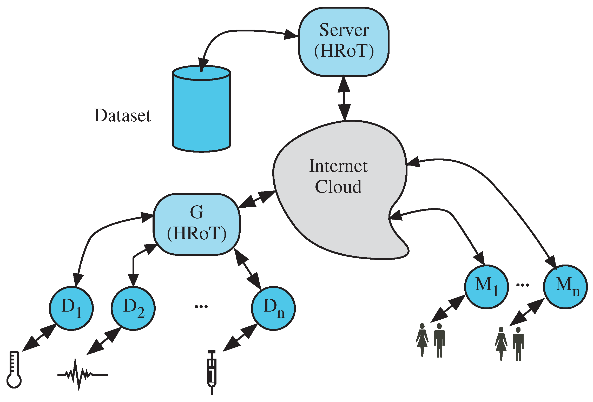
:1. Introduction and Related Work
2. Algorithm of Interleaved Modular Multiplication
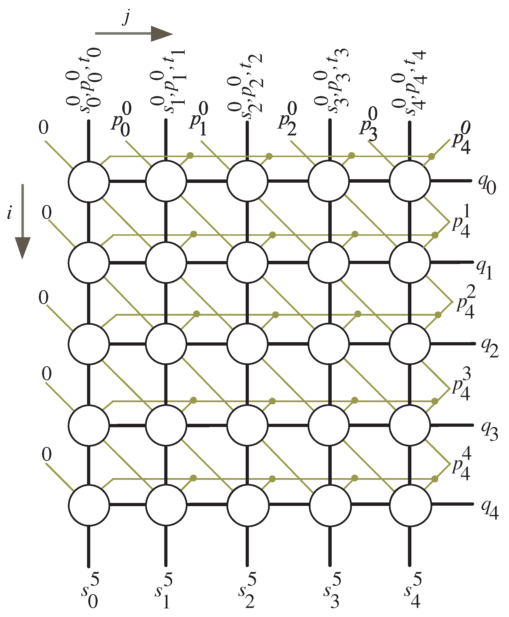
Dependency Graph
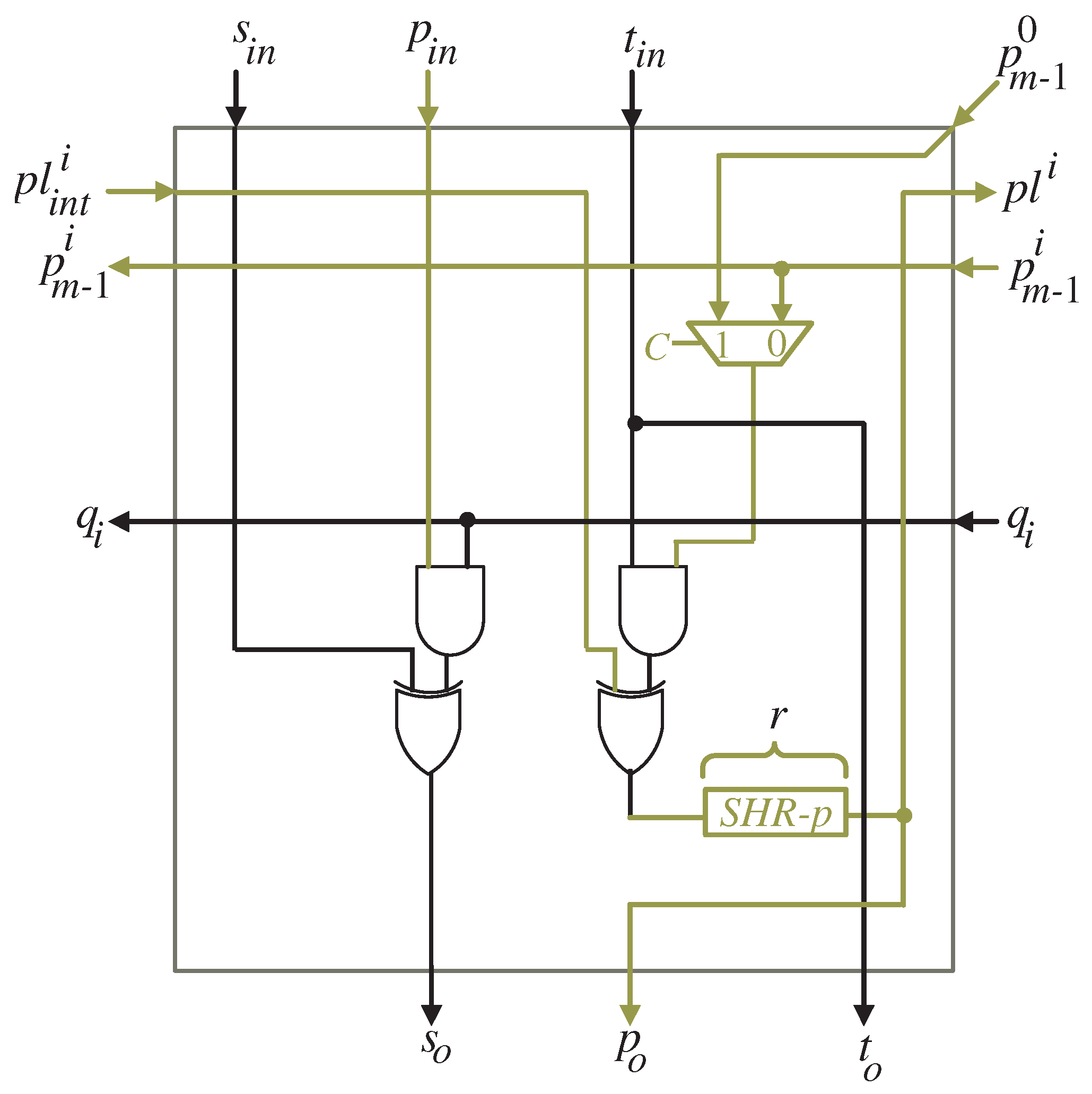
3. Word-Serial Accelerator Structure Exploration
3.1. Scheduling Function
3.2. Projection Function
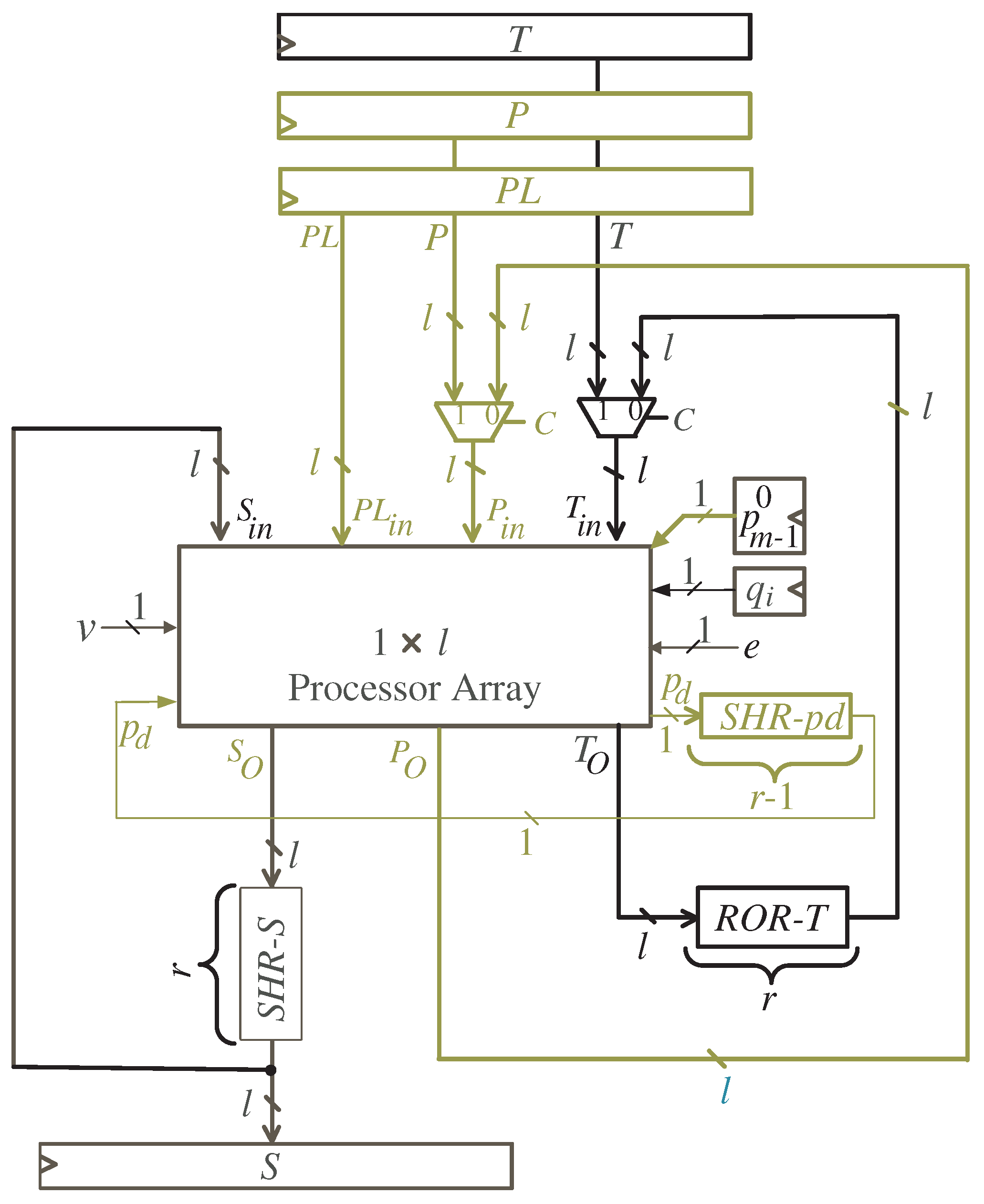
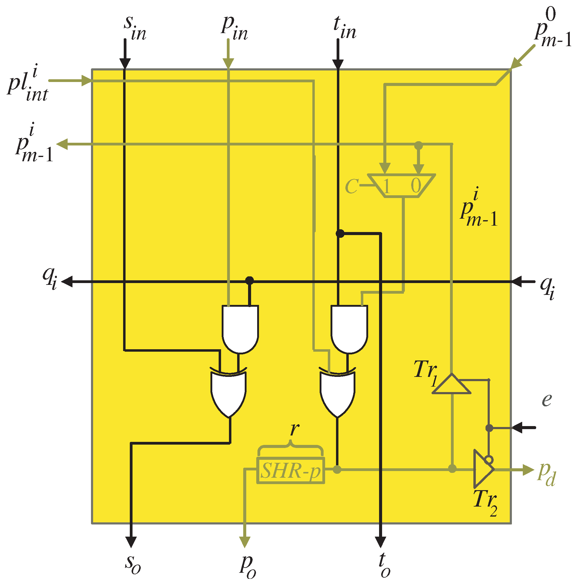
- A processor array block whose word size is l;
- Three input registers T, P and ;
- One output register S;
- Three shift-right registers SHR-S, SHR-pd and SHR-P (which is inside the processor array block);
- Rotate-right register ROR-T;
- Four three-input MUXes (two of them inside the processor array block) to select between the inputs and partial results of variables P and T.
- Control signal C, controlling the selection of all MUXes, activates () during the the first clock cycles to feed the input words of operands T, P, and to all PEs of the processor array block. The words are fed starting with the most significant words. Moreover, the most significant bit is passed to the last PE, , and broadcasted to the remaining PEs. At the first clock cycle, SHR-S is cleared to initialize the S variable with zero values.
- Control signal C of all MUXes deactivates () during the remaining clock cycles to feed the resulted intermediate words of P and fixed words of T to all PEs of the processor array block. These words are passed through shift-registers SHR-P, SHR-pd, and RoT-T, respectively. Moreover, the resulted intermediate words of S are fed to all PEs of the processor array block through the shift-register SHR-S.
- Control signal e activates () at the clock cycles , , to enable the tri-state buffer shown in Figure 6 to horizontally feed the bits of , , to the remaining PEs. Moreover, input bits are broadcasted during the same clock cycles to all PEs in the processor array block. The control signal e deactivates () during the remaining clock cycles to enable the tri-state buffer , displayed in Figure 6, to feed the bits of through the shift-register SHR-pd to the input of the processor array block as shown in Figure 4.
- Control signal v, shown in Figure 5, deactivates () at clock cycles , , to force zero bit values to the P words shown at the leftmost side of the DG, Figure 3. Control signal v activates () at the remaining clock cycles to feed the signal through the leftmost MUX of the processor array shown in Figure 5.
- The resulting output words S are available at the output bus, through register S shown in Figure 4, during clock cycles .
4. Complexities Analysis
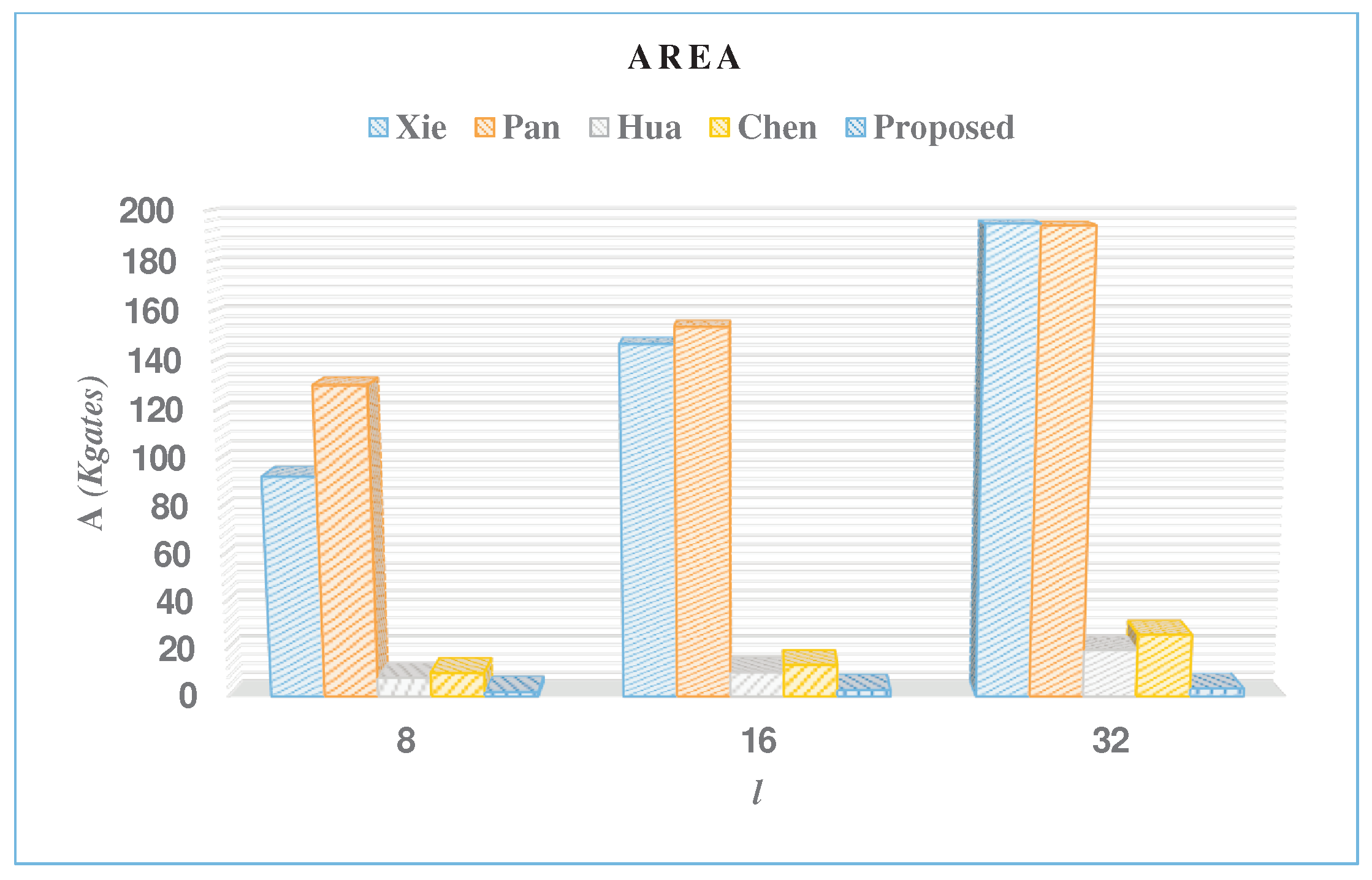
- Area (A) results are obtained in terms of the two-input NAND gate and are represented in units of kilo-gates .
- Total computation time (T) is represented in nano-second time unit.
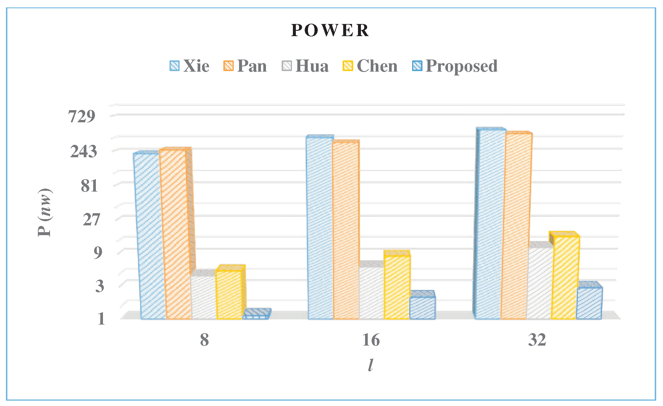
- Consumed power (P) is obtained at a frequency of 1 KHz in units of milliwatt .
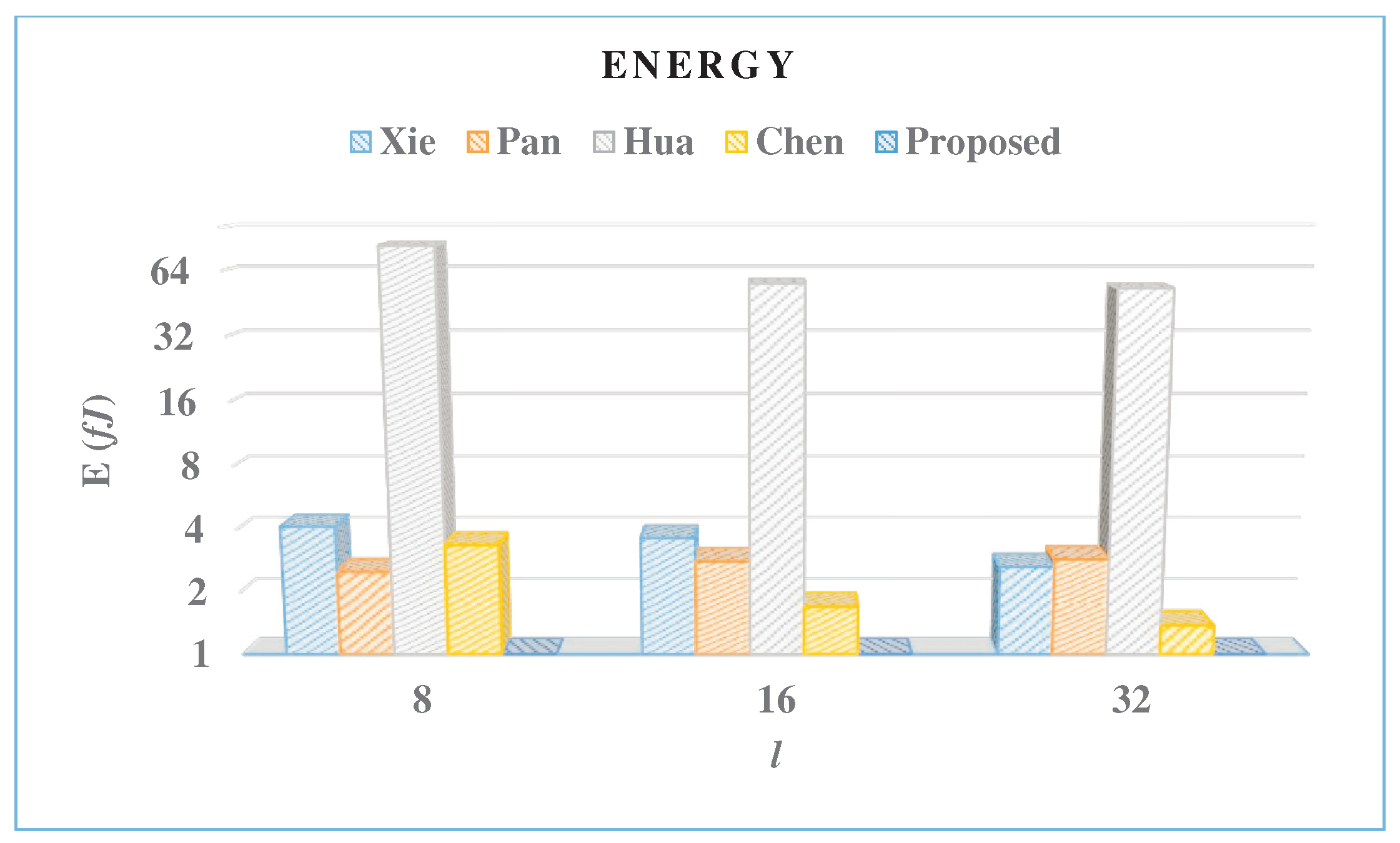
- Consumed energy (E) is obtained as the product of P and T in units of femtojoule
- Area–time product (AT) is obtained as the product of A and T in units of kgates–nanosecond
- (i)
- At word-size , the multiplier that achieves the lowest AT is the multiplier of Pan [9]. It outperforms the proposed design by %27.8 at this word size. On the other hand, the proposed multiplier outperforms the other multipliers in AT at this word size, achieving a maximum reduction of 98.9% over the design of Hua [11].
- (ii)
- At word-sizes and , the proposed multiplier achieves the lowest AT than the other multiplier structures due to the significant reduction of its latency and computation time at these word sizes. As we notice from Table 1, the latency of the proposed multiplier is inversely proportional to the word size l. As a result, the latency significantly decreases as the word size l increases.
5. Summary and Conclusions
Author Contributions
Funding
Institutional Review Board Statement
Informed Consent Statement
Data Availability Statement
Acknowledgments
Conflicts of Interest
Abbreviations
| IoT | Internet of Things |
| ASIC | Application Specific Integrated Circuit |
| ECC | elliptic curve cryptography |
| DG | dependency graph |
| VLSI | very large scale integrated circuit |
| RSA | Rivest, Shamir, and Adleman |
| CPD | critical path delay |
References
- Pourghebleh, B.; Hayyolalam, V.; Anvigh, A.A. Service discovery in the Internet of Things: Review of current trends and research challenges. Wirel. Netw. 2020, 26, 5371–5391. [Google Scholar] [CrossRef]
- Anajemba, J.H.; Iwendi, C.; Mittal, M.; Yue, T. Improved advance encryption standard with a privacy database structure for IoT nodes. In Proceedings of the 2020 IEEE 9th International Conference on Communication Systems and Network Technologies (CSNT), Gwalior, India, 10–12 April 2020; pp. 201–206. [Google Scholar]
- Mittal, M.; Vijayal, S. Detection of attacks in IoT based on ontology using SPARQL. In Proceedings of the 2017 7th International Conference on Communication Systems and Network Technologies (CSNT), Nagpur, India, 11–13 November 2017; pp. 206–211. [Google Scholar]
- Anajemba, J.H.; Yue, T.; Iwendi, C.; Alenezi, M.; Mittal, M. Optimal cooperative offloading scheme for energy efficient multi-access edge computation. IEEE Access 2020, 8, 53931–53941. [Google Scholar] [CrossRef]
- NIST. Post-Quantum Cryptography, Round 2 Submissions. Available online: https://csrc.nist.gov/projects/post-quantum-cryptography/round-2-submissions (accessed on 9 December 2020).
- Kim, K.W.; Jeon, J.C. Polynomial Basis Multiplier Using Cellular Systolic Architecture. IETE J. Res. 2014, 60, 194–199. [Google Scholar] [CrossRef]
- Choi, S.; Lee, K. Efficient systolic modular multiplier/squarer for fast exponentiation over GF(2m). IEICE Electron. Express 2015, 12, 20171195. [Google Scholar] [CrossRef] [Green Version]
- Kim, K.W.; Kim, S.H. Efficient bit-parallel systolic architecture for multiplication and squaring over GF(2m). IEICE Electron. Express 2018, 15, 1–6. [Google Scholar] [CrossRef] [Green Version]
- Pan, J.S.; Lee, C.Y.; Meher, P.K. Low-Latency Digit-Serial and Digit-Parallel Systolic Multipliers for Large Binary Extension Fields. IEEE Trans. Circ. Sys.-I 2013, 60, 3195–3204. [Google Scholar] [CrossRef]
- Xie, J.; Meher, P.K.; Mao, Z. Low-latency high-throughput systolic multipliers over GF(2m) for NIST recommended pentanomials. IEEE Trans. Circuits Syst. 2015, 62, 881–890. [Google Scholar] [CrossRef]
- Hua, Y.Y.; Lin, J.M.; Chiou, C.W.; Lee, C.Y.; Liu, Y.H. Low Space-Complexity Digit-Serial Dual Basis Systolic Multiplier over GF(2m) Using Hankel Matrix and Karatsuba Algorithm. IET Inf. Secur. 2013, 7, 75–86. [Google Scholar]
- Chen, C.C.; Lee, C.Y.; Lu, E.H. Scalable and Systolic Montgomery Multipliers Over GF(2m). IEICE Trans. Fundam. Electron. Commun. Comput. Sci. 2008, E91-A, 1763–1771. [Google Scholar] [CrossRef]
- Talapatra, S.; Rahaman, H.; Mathew, J. Low complexity digit serial systolic montgomery multipliers for special class of GF(2m). IEEE Trans. Very Large Scale Integr. (VLSI) Syst. 2010, 18, 847–852. [Google Scholar] [CrossRef]
- Guo, J.H.; Wang, C.L. Hardware-efficient Systolic Architecture for Inversion and Division in GF(2m). IEE Proc. Comput. Digit. Tech. 1998, 145, 272–278. [Google Scholar] [CrossRef]
- Lee, C.Y.; Fan, C.C.; Yuan, S.M. New Digit-Serial Three-Operand Multiplier over Binary Extension Fields for High-Performance Applications. In Proceedings of the 2017 2nd IEEE International Conference on Computational Intelligence and Applications, Beijing, China, 8–11 September 2017; pp. 498–502. [Google Scholar]
- Chen, L.H.; Chang, P.L.; Lee, C.Y.; Yang, Y.K. Scalable and systolic dual basis multiplier Over GF(2m). Int. J. Innov. Comput. Inf. Control 2011, 7, 1193–1208. [Google Scholar]
- Bayat-Sarmadi, S.; Kermani, M.M.; Azarderakhsh, R.; Lee, C.Y. Dual-Basis Superserial Multipliers for Secure Applications and Lightweight Cryptographic Architectures. IEEE Trans. Circ. Sys.-II 2014, 61, 125–129. [Google Scholar] [CrossRef]
- Gebali, F.; Ibrahim, A. Efficient Scalable Serial Multiplier Over GF(2m) Based on Trinomial. IEEE Trans. Very Large Scale Integr. (VLSI) Syst. 2015, 23, 2322–2326. [Google Scholar] [CrossRef]
- Ibrahim, A.; Gebali, F. Scalable and Unified Digit-Serial Processor Array Architecture for Multiplication and Inversion over GF(2m). IEEE Trans. Circuits Syst. I Regul. Pap. 2017, 22, 2894–2906. [Google Scholar] [CrossRef]
- Kim, K.W.; Lee, J.D. Efficient unified semi-systolic arrays for multiplication and squaring over GF(2m). IEICE Electron. Express 2017, 14, 1–10. [Google Scholar] [CrossRef] [Green Version]
- Gebali, F. Algorithms and Parallel Computers; John Wiley: New York, NY, USA, 2011. [Google Scholar]
- Ibrahim, A.; Alsomani, T.; Gebali, F. Unified Systolic Array Architecture for Field Multiplication and Inversion Over GF(2m). Comput. Electr. Eng. J.-Elsevier 2017, 61, 104–115. [Google Scholar] [CrossRef]
- Ibrahim, A. Efficient Parallel and Serial Systolic Structures for Multiplication and Squaring Over GF (2m). Can. J. Electr. Comput. Eng. 2019, 42, 114–120. [Google Scholar] [CrossRef]


| Multiplier | Tri-State | AND | XOR | MUXes | Flip-Flops | Latency | CPD |
|---|---|---|---|---|---|---|---|
| Xie [10] | 0 | 0 | |||||
| Pan [9] | 0 | 0 | |||||
| Hua [11] | 0 | 0 | |||||
| Chen [12] | 0 | ||||||
| Proposed | 2 |
| Multiplier | l | A | T | P | E | AT | %A | %AT | %P | %E |
|---|---|---|---|---|---|---|---|---|---|---|
| [Kgates] | [ns] | [mW] | [fJ] | |||||||
| Xie [10] | 8 | 92.9 | 18.3 | 225.6 | 4.1 | 1698.7 | 97.9 | 31.8 | 99.5 | 76.5 |
| 16 | 147 | 9.7 | 375.5 | 3.6 | 1425.9 | 98.1 | 15.0 | 99.4 | 75 | |
| 32 | 195.1 | 5.5 | 477.4 | 2.6 | 1078.9 | 98.3 | 31.8 | 99.4 | 76.1 | |
| Pan [9] | 8 | 130.5 | 9.9 | 252.9 | 2.5 | 1291.6 | 98.5 | −27.3 | 99.6 | 61.2 |
| 16 | 153.9 | 8.8 | 320.1 | 2.8 | 1354.6 | 98.2 | 10.5 | 99.3 | 67.7 | |
| 32 | 194.3 | 6.8 | 425.1 | 2.9 | 1317.6 | 98.3 | 44.2 | 99.3 | 78.1 | |
| Hua [11] | 8 | 7.9 | 19,053.5 | 4.4 | 82.9 | 152,237.2 | 76.2 | 98.9 | 74.3 | 98.8 |
| 16 | 10.4 | 9526.7 | 5.9 | 55.7 | 99,077.9 | 73.1 | 98.8 | 64.1 | 98.4 | |
| 32 | 19.9 | 4763.3 | 11.2 | 53.1 | 94,838.7 | 82.9 | 99.2 | 73.9 | 98.8 | |
| Chen [12] | 8 | 10.2 | 659.4 | 5.1 | 3.4 | 6699.7 | 81.3 | 75.5 | 78.1 | 71.2 |
| 16 | 13.5 | 203.0 | 8.4 | 1.7 | 2742.9 | 79.3 | 55.8 | 74.9 | 46.5 | |
| 32 | 26.6 | 86.8 | 15.9 | 1.4 | 2306.3 | 87.2 | 68.1 | 81.8 | 54.3 | |
| Proposed | 8 | 1.9 | 865.6 | 1.1 | 0.97 | 1644.6 | - | - | - | - |
| 16 | 2.8 | 432.8 | 2.1 | 0.91 | 1211.8 | - | - | - | - | |
| 32 | 3.4 | 216.4 | 2.9 | 0.6 | 735.8 | - | - | - | - |
Publisher’s Note: MDPI stays neutral with regard to jurisdictional claims in published maps and institutional affiliations. |
© 2022 by the authors. Licensee MDPI, Basel, Switzerland. This article is an open access article distributed under the terms and conditions of the Creative Commons Attribution (CC BY) license (https://creativecommons.org/licenses/by/4.0/).
Share and Cite
Ibrahim, A.; Gebali, F. Compact Word-Serial Modular Multiplier Accelerator Structure for Cryptographic Processors in IoT Edge Nodes with Limited Resources. Mathematics 2022, 10, 848. https://doi.org/10.3390/math10050848
Ibrahim A, Gebali F. Compact Word-Serial Modular Multiplier Accelerator Structure for Cryptographic Processors in IoT Edge Nodes with Limited Resources. Mathematics. 2022; 10(5):848. https://doi.org/10.3390/math10050848
Chicago/Turabian StyleIbrahim, Atef, and Fayez Gebali. 2022. "Compact Word-Serial Modular Multiplier Accelerator Structure for Cryptographic Processors in IoT Edge Nodes with Limited Resources" Mathematics 10, no. 5: 848. https://doi.org/10.3390/math10050848
APA StyleIbrahim, A., & Gebali, F. (2022). Compact Word-Serial Modular Multiplier Accelerator Structure for Cryptographic Processors in IoT Edge Nodes with Limited Resources. Mathematics, 10(5), 848. https://doi.org/10.3390/math10050848