Article

Oxide Thin-Film Transistors on Fibers for Smart Textiles

1
Sensor Technology Research Centre, University of Sussex, Falmer BN1 9QT, UK
2
Electronics Laboratory, Swiss Federal Institute of Technology, Zürich 8092, Switzerland
*
Author to whom correspondence should be addressed.
Technologies 2017, 5(2), 31; https://doi.org/10.3390/technologies5020031
Submission received: 30 April 2017 / Revised: 26 May 2017 / Accepted: 29 May 2017 / Published: 2 June 2017
(This article belongs to the Special Issue Wearable Technologies)

Abstract

:
Smart textiles promise to have a significant impact on future wearable devices. Among the different approaches to combine electronic functionality and fabrics, the fabrication of active fibers results in the most unobtrusive integration and optimal compatibility between electronics and textile manufacturing equipment. The fabrication of electronic devices, in particular transistors on heavily curved, temperature sensitive, and rough textiles fibers is not easily achievable using standard clean room technologies. Hence, we evaluated different fabrication techniques and multiple fibers made from polymers, cotton, metal and glass exhibiting diameters down to 125 μm. The benchmarked techniques include the direct fabrication of thin-film structures using a low temperature shadow mask process, and the transfer of thin-film transistors (TFTs) fabricated on a thin (≈1 μm) flexible polymer membrane. Both approaches enable the fabrication of working devices, in particular the transfer method results in fully functional transistor fibers, with an on-off current ratio > 10 7 , a threshold voltage of ≈0.8 V , and a field effect mobility exceeding 7 c m 2 V 1 s 1 . Finally, the most promising fabrication approach is used to integrate a commercial nylon fiber functionalized with InGaZnO TFTs into a woven textile.

1. Introduction

Electronic or smart textiles (e-textiles) promise to have a significant impact in areas such as wearable computing or large-area electronics [1]. Potential areas of application include healthcare, sports, or support of high risk professionals, e.g., firefighters [2,3,4]. Here, the vision is of an e-textile consisting of a fabric that preserves all the properties of textile fibers, such as comformability, washability, softness or stretchability, and combines them with electronic functionality. The aforementioned electronic functionality often refers to different sensors e.g., for strain, posture, temperature or other physiological signals [5,6] but also includes the associated conditioning circuits, power supply, and signal processing or transmission electronics [7,8,9]. So far, the spectrum of e-textiles ranges from conventional electronics attached to textiles [10] to electronic components build from active textile yarns [11,12]. The first approach, usually realized by integrating rigid off-the-shelf electrical devices and circuit boards, drastically influences the mechanical properties of the textile, while, the second one in general only provides limited electronic complexity and hence limited electronic performance [13]. An alternative approach is the integration of flexible electronics into a woven textile. Here, the use of flexible plastic stripes as carriers for thin-film devices and standard silicon chips, represents a good compromise between the mechanical and electrical properties of the final textile device [14]. Additionally, the integration of electronic fibers and conductive yarns in the weft and warp direction of a woven fabric also enables the fabrication of more complex systems inside a textile. Nevertheless, the integration of flexible stripes causes another fabric specific problem which is in particular important concerning the mass production of electronic textiles: Non-circular fibers such as planar plastic stripes are not compatible with standard weaving equipment, and are sensitive to twisting which calls for modified knitting or embroidery machines [15].
The solution to this problem is the fabrication of mechanically flexible active electronic devices directly on circular fibers. Since the fabrication of electronic devices on fibers, compatible with the demands of the textile industry, is challenging only few associated reports including a temperature sensor on a nylon yarn have been published [16]. In this context, the fabrication related challenges arise from the required flexibility, and the chemical and physical proprieties of the available yarns. Additionally, yarns usable for the fabrication of textiles exhibit diameters significantly below 1 m m , which results in a highly curved surface. These challenges can be addressed by new developments in the area of flexible electronics. In particular the use of oxide semiconductors, such as amorphous InGaZnO (IGZO) [17,18,19], promises to realize high performance active electronic devices on a variety of substrates. Here, we evaluated how IGZO thin-film transistors (TFTs), representing the most important and basic building block of all electronic systems, can be fabricated on a variety of different yarns. It is shown that high performance TFTs, on glass fibers with a radius of 62.5 μm and on polymer fibers with a radius of 125 μm, are fully functional and can be integrated into textiles for wearable or industrial applications.

2. Fabrication of TFTs on Fibers

In contrast to conventional substrates used for the fabrication of electronic thin-film devices, such as semiconductor wafers, glass plates or plastic foils, the mechanical and geometrical properties of fibers and yarns are less beneficial. Hence, the successful fabrication of transistors requires a modification of the fabrication process and a proper selection of suitable yarns or fibers. Here, technologies developed for the fabrication of flexible and stretchable electronics are adapted.

2.1. Micro Processing on Yarns and Fibers

We evaluated a range of possible substrate fibers. As shown in Figure 1a, these included steel and cotton yarns, nylon fibers with different diameters, glass fibers, and thin insulated metal Cu (magnet) wire. All materials have certain advantages and disadvantages concerning the fabrication of smart textiles. The most important parameters for the fabrication of TFTs and electronic textiles are:
  • Chemical properties: The chemical stability of the fiber material is a key aspect since the fibers have to resist the etchants and solvents used during the fabrication process. In this respect the metal and glass fibers exhibit the most beneficial properties.
  • Temperature resistance: Similar to the chemical properties, the melting or glass transition temperature of the evaluated materials can significantly limit the choice of usable deposition technologies. While the maximum temperature of cotton and nylon is in the range of 200 C , the glass fiber can be processed at temperatures above 1000 C .
  • Fiber surface: Thin-film devices are made from active layers with thickness in the nanometer range, hence the surface of the fibers has to be as flat as possible. While the steel and cotton yarns do not exhibit a continuous surface, also the surface roughness of the other fibers varies strongly. The rms value of the employed glass fibers is <10 n m , but the corresponding values for nylon and the insulated Cu wire reach values of 10 μm and 1 μm, respectively.
  • Conductivity: Non-conductive fibers (glass, cotton, nylon) have the advantage that no additional insulation layer is needed, and all electronic devices on their surface are decoupled from each other. Metallic substrate fibers at the same time, could simplify the device structure by providing electronic functionality themselves. Here an interesting option could be the use the insulated Cu wire as substrate fiber, gate contact and gate insulator simultaneously.
  • Textile properties: Unobtrusive smart textiles call for electronic fibers which are soft, bendable, and with dimensions comparable to the textile yarns of the fabric. In this respect cotton but also steel yarns have beneficial properties. Similarly, polymer fibers such as nylon are common. Anyway, the diameter of the nylon fibers should not be too large (≲750 μm [20]). Furthermore, thin Cu wires are bendable and can be imperceptible when integrated into a textile [21]. Glass fibers on the other hand exhibit a small diameter, but their minimum bending radius is limited to ≈5 c m .
In total it can be concluded that the continuous cylindrical shape, the wide availability, the variable diameter, the mechanical flexibility, and its use in commercial textiles makes nylon the most suitable choice for the fabrication of electronic fibers. At the same time, the high surface roughness of commercial nylon fibers remains an issue.
Another issue which has to be considered is the extreme form factor (relation between diameter and length) of all kinds of fibers. First it has to be mentioned that the most effective solution for the fabrication of long functionalized fibers, desirable for the fabrication of textiles, would be roll-to-roll fabrication [22]. Specialized equipment to continuously coat fibers has been developed using for example sputtering techniques [23]. Loading a fiber into a commercial semiconductor processing tool, and structuring the deposited layers, in general requires the use of a carrier substrate to provide mechanical support and to simplify the handling of the fiber during the fabrication process. Here we considered three basic possibilities, illustrated in Figure 1b, to ensure comparability between the substrate fibers and the processing equipment. Mounting short fibers upright on the carrier enables a 360° coating of the fibers, but also limits their length which is contradictory to their use in a textile. Coiling up the fiber on the surface of a carrier allows processing of longer fibres, the disadvantages are that only one halve of the fiber surface (top side) is coated, and that there is mechanical strain induced all along the fiber. Finally wrapping the fiber around a carrier substrate can be used for very long fibers (a 3 inch carrier substrate in combination with a 250 μm fiber and a 50% fill factor results in a max fiber length of ≈20 m ). The disadvantages are that again only one halve of the fiber surface can be coated, and that the fiber on the back of the carrier substrate is not coated at all.

2.2. Fabrication Approaches

To determine the most appropriate manufacturing process, we evaluated two different approaches to fabricate TFTs on fibers: The direct fabrication of devices on nylon and glass fibers using standard semiconductor manufacturing equipment [18], and the transfer of TFTs, fabricated on flat and thin substrates, to different fibers, and yarns [24]. During the direct fabrication process the fibers were loaded into the deposition tools by wrapping them around the carrier or using only short (≈6 c m ) fibers attached to a carrier.

2.2.1. Direct Fabrication

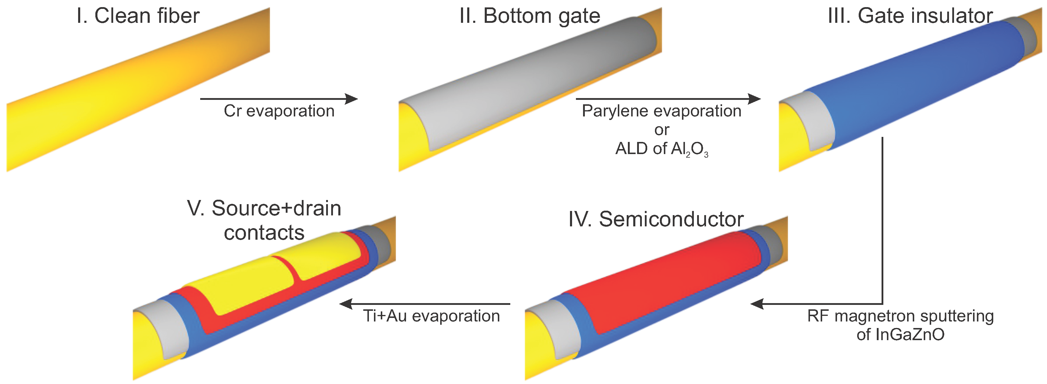
Direct fabrication was performed on nylon and glass fibers. The schematic process flow is illustrated in Figure 2. Depending on the material, fibers were cleaned using water, acetone, IPA, and sonication. Next, a Cr bottom gate was electron beam evaporated, here the sample was tilted and rotated to ensure a uniform coating of the curved surface. The bottom gate was then insulated by the deposition of a dielectric material. First we used atomic layer deposition (ALD) at 150 C to grow 100 n m of A l 2 O 3 . In case of the glass fibers this resulted in an insulating layer, but the high surface roughness of nylon prevented the formation of a pinhole free layer on the nylon fibers. Since ALD is not suitable for the deposition of thicker layers, the nylon fibers were insulated by depositing a 1 μm thick film of parylene. Subsequent to the insulation of the gate, 30 n m of amorphous IGZO was deposited using a radio frequency (RF) magnetron sputtering process based on a ceramic I n G a Z n O 4 target and a pure Ar sputtering atmosphere at a pressure of 2 m Torr. The fabrication process was finalized by the deposition of the source and drain contacts. 10 n m of titanium, acting a adhesion layer, and 75 n m of gold were electron beam evaporated. Structuring of all layers was done using a shadow mask. This is because of the geometry of the fibers, and also due to the limited chemical resistance of nylon fibers. Here, low resolution shadow masks were hand cut from aluminum foil, whereas high resolution (≈100 μm) shadow masks were etched from a polyimide foil structured using conventional lithography [25].

2.2.2. Transfer Fabrication

Another possibility to overcome the process related limitations caused by the mechanical, chemical and geometrical properties of the different fibers is to fabricate TFTs on a conventional flexible substrate and then transfer them onto a fiber or yarn. This approach was evaluated by fabricating passivated IGZO based bottom gate inverted staggered TFTs on a Si wafer covered with a spin coated 400 n m Polyvinyl alcohol (PVA) sacrificial layer and an evaporated 1 μm thin parylene membrane. The TFTs itself were fabricated by evaporating 35 n m Cr, insulated by an ALD deposited 25 n m A l 2 O 3 layer, acting as bottom gate; RF sputtering of 15 n m amorphous IGZO; and the evaporation of 60 n m Au (here, an underlying 15 n m thick Ti layer acts as adhesion layer) as source and drain contacts. Furthermore an additional 25 n m A l 2 O 3 layer is used as back-channel passivation. All layers were structured by standard optical lithography. The detailed fabrication process is described elsewhere [24]. After the fabrication, the PVA sacrificial layer is dissolved in water, and the resulting free standing electronic membrane can then be cut and transferred to a fiber. Nylon fibers with radii of 500 μm and 250 μm as well as yarns are used as final substrate. Here the low thickness of the parylene membrane ensures that even the small bending radii caused by wrapping the transistors around a fiber with diameter 250 μm, cannot cause mechanical strain larger than 0.5%. The reason for this is the direct proportionality between substrate thickness and strain induced by bending. This in return guaranties the full functionality of the transistors. The transfer process is visualized in Figure 3a. To promote the adhesion between the parylene and the nylon, a commercial two component polymercaptan/epoxy adhesive was used. The surface tension of the adhesive also prevented any wrinkling of the parylene membrane. Figure 3b illustrates the structure of the resulting functionalized fibers.

3. Results and Discussion

Electrical characterization of the fiber TFTs was performed inside a shielded probe station under ambient conditions using a Keysight B1500A parameter analyzer. Performance parameters were extracted using the Shichman-Hodges equations to model the field effect transistor drain current in the saturation regime [26].

3.1. Directly Fabricated TFTs

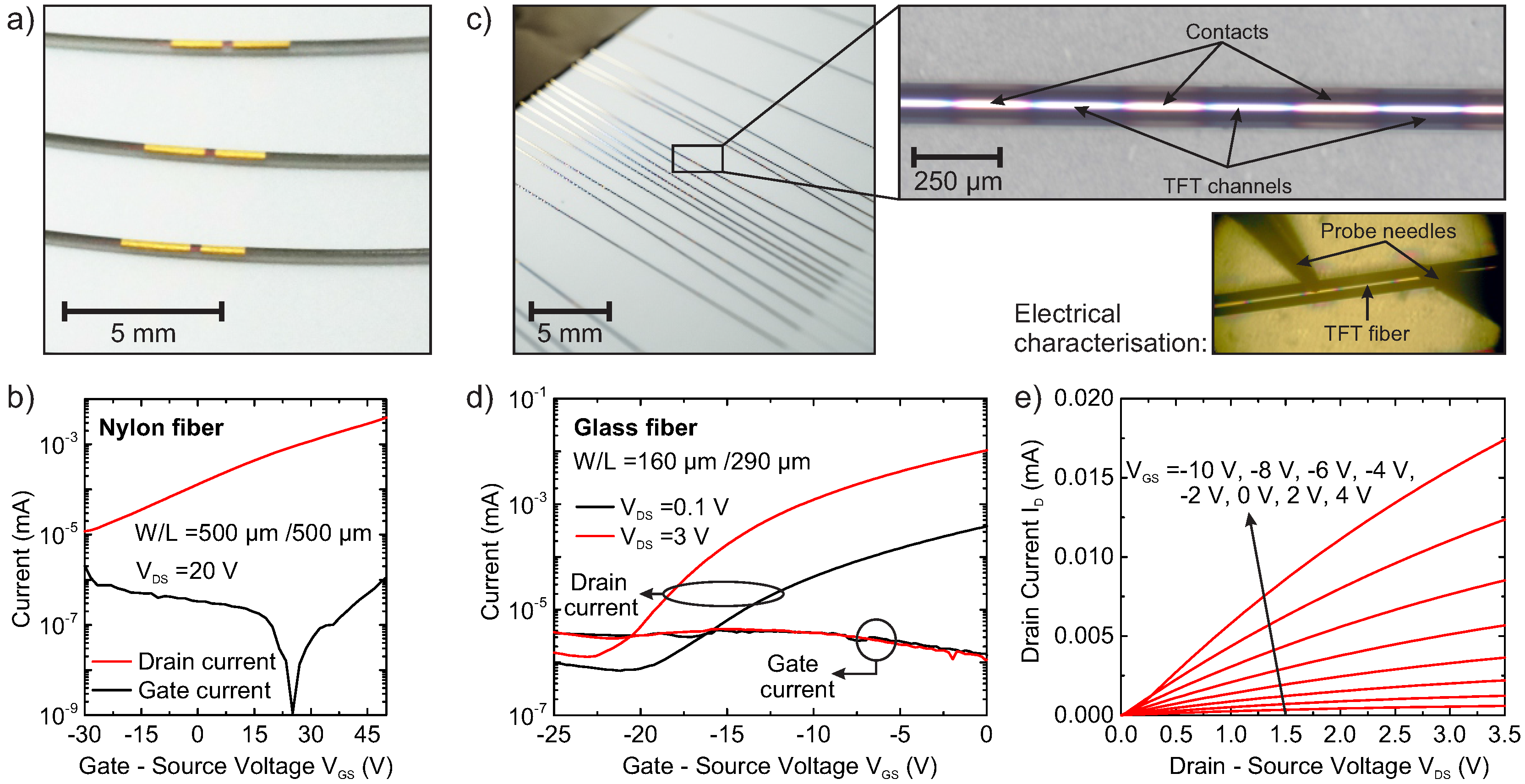
The IGZO TFTs, directly fabricated on nylon and glass fibers, are presented in Figure 4. Multiple TFTs have been fabricated on a single fiber, where a common gate was used for all TFTs on one fiber.

3.1.1. TFTs on Polymer Fibers

Figure 4a,b show a photograph and the associated V G S -I D transfer characteristic of the nylon fiber TFTs. As mentioned above the main obstacle concerning the TFT fabrication on nylon fibers is the high surface roughness of nylon. To effectively insulate the gate from the transistor channel it was necessary to deposit a 1 μ m thick parylene layer as gate insulator. This in combination with the low dielectric constant of parylene (3.06) [27] lead to a very low gate capacitance of ≈27 μ F m 2 . Hence, the resulting TFTs exhibit only a low on-off current ratio of ≈ 3 × 10 2 even if the gate-source voltage is swept between −30 V and 47.5 V . At the same time it has to be mentioned that even at high voltages like this, the gate current stays below 10 9 A . Nevertheless, under the applied gate-source voltages the TFTs are only operated in the subthreshold regime, which excludes the extraction of any meaningful quantitative performance parameters. These results show that the direct fabrication of TFTs on a commercial nylon fiber seems possible. Nevertheless the problems associated to the surface roughness, such as the required thickness of the gate insulator, and hence the high operation voltages, exclude any useful application as long as no better dielectric is found.

3.1.2. TFTs on Glass Fibers

To reduce the operation voltage of the fiber TFTs the gate capacitance has to be increased. Since the deposition of significantly thinner gate insulators is not possible on the employed nylon, glass fibers have been used to prove the concept. The smooth surface and higher temperature resistance of glass allowed the fabrication of functional TFTs using only 100 n m of A l 2 O 3 , exhibiting a dielectric constant of 9.5, as gate insulator. Figure 4c displays photographs and micrographs of the resulting transistors. The corresponding transfer and output characteristics of a representative TFT are shown in Figure 4d,e, respectively. The transistor operated in depletion mode and exhibits a threshold voltage of −12.5 V , a field effect mobility of 3 c m 2 V 1 s 1 , an on-off current ratio of 10 4 , and a maximum transconductance of 1.7 μ S . Compared to the nylon fiber transistors, these performance parameters show a significant improvement, nonetheless in particular the very negative threshold voltage is not desirable. This is because, for wearable applications, enhancement mode transistors operating at voltages below 5 V are preferred. The reason for the negative threshold voltage is the lack of a back channel passivisation, and the fact that all process steps are performed at room temperature (hence there is no intentional or unintentional annealing of the semiconductor). It is expected that the deposition of an additional A l 2 O 3 passivation layer would be beneficial, but structuring and precise alignment of small contact holes on the source and drain contacts using a shadow mask is challenging (the performed structuring of the gate insulator is significantly less demanding). At the same time, fabrication of passivated TFTs using the transfer approach, described in the next paragraph, is easily possible.

3.2. Transferred TFTs

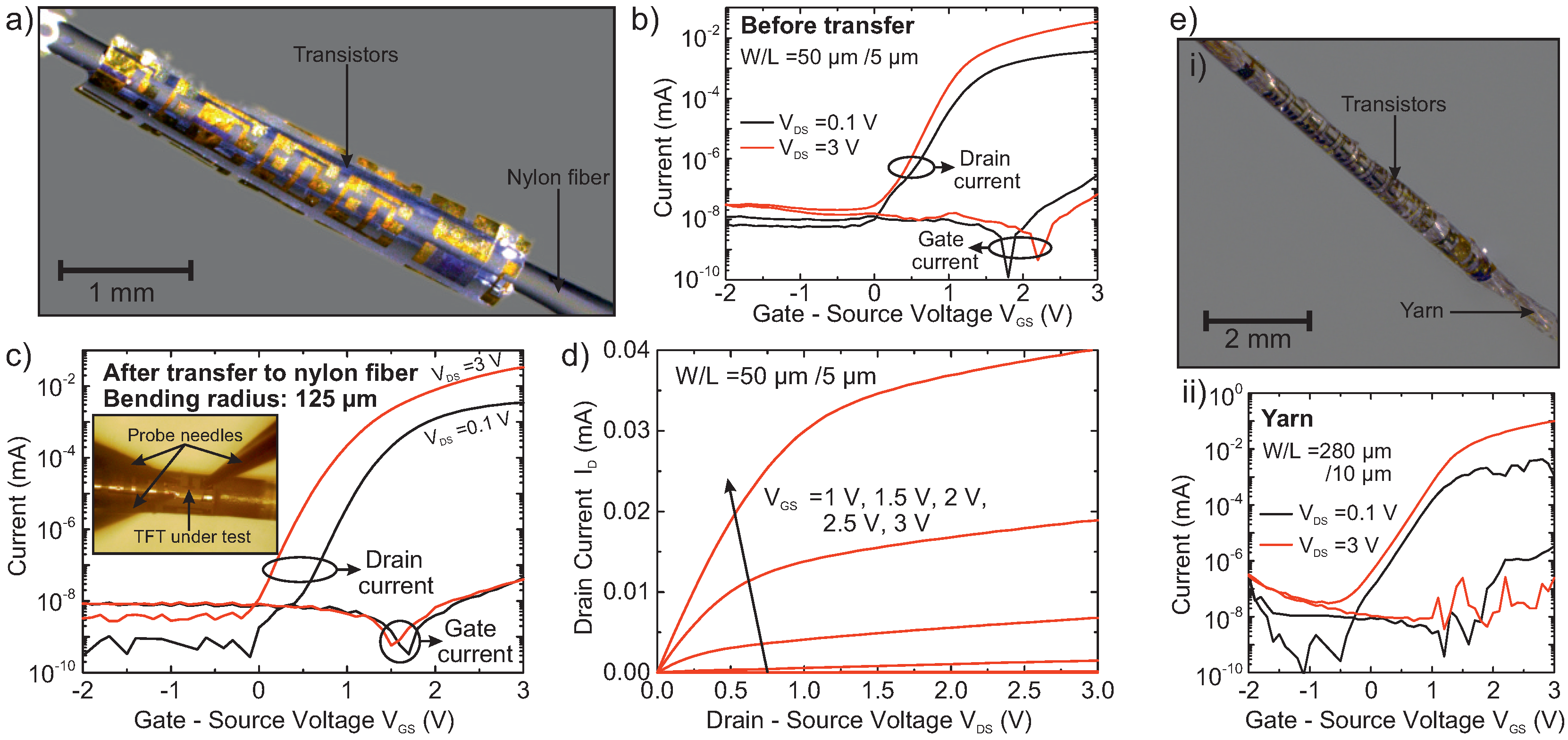
Figure 5 presents transistors on nylon fibers and yarns fabricated using the transfer approach. A micrograph of a functionalized nylon fiber with a diameter of 250 μ m is shown in Figure 5a. A representative TFT has been characterized directly before and after it was transferred to the fiber. The transfer characteristic of the transistor measured on the silicon carrier wafer (Figure 5b) and when permanently attached to the fiber (Figure 5c) shows that the transistor operates in the enhancement mode. On the fiber, the TFTs exhibits a threshold voltage of 0.85 V (−0.1 V compared to the measurement before transfer), a field effect mobility of 7.2 c m 2 V 1 s 1 (+4%), an on-off current ratio of 10 7 (×8), and a maximum transconductance of 52.1 μ S (+7.2%). The improvement of the transistor performance is associated to tensile mechanical strain induced by bending the TFT around the fiber. In case of IGZO TFTs this strain increased the effective carrier mobility and decreases the threshold voltage [28]. The corresponding output characteristic of the same transistor measured on the fiber is plotted in Figure 5d, here a clear current saturation effect is visible.
In addition to the use of nylon fibers, Figure 5e illustrates that it is also possible to fabricate functionalized yarns using the transfer approach. Here, a transistor on a multi-thread yarn with a variable diameter between 100 μ m and 250 μ m is shown. The corresponding TFT transfer characteristic is used to extract the performance parameters. The noise visible in the measurement of the linear transistor regime (V D S = 0.1 V ) is caused by the uneven and soft surface of the yarn. This soft surface prevents the formation of a reliable and stable contact between the device and the probe needles, which also leads to an increase of the contact resistance. On the yarn the transistor exhibits a threshold voltage of 0.8 V , a field effect mobility of 4.6 c m 2 V 1 s 1 , an on-off current ratio of 10 6 , and a maximum transconductance of 93 μ S , which confirms the full electronic functionality of the TFT.

4. Conclusions

We compared different fibers, yarns and thin-film manufacturing technologies and evaluated their suitability for the fabrication of TFTs on textile fibers with diameters down to 125 μ m . The direct fabrication of bottom gate transistors based on amorphous IGZO on nylon and glass fibers is possible. Here, the chemical properties, and the surface roughness of commercial textile fibers degrade the performance of these transistors which makes it difficult to achieve low voltage operation and high flexibility simultaneously. At the same time, fabricating transistors on nylon fibers and yarn using a transfer approach makes it possible to use standard fabrication technologies and to realize functionalized fibers compatible with large scale textile manufacturing equipment. In this respect, transferring IGZO TFTs from a flat substrate to an arbitrary fiber or yarn results in high performance transistors with field effect mobilities up to 7.2 c m 2 V 1 s 1 . Furthermore, an additional advantage of the transfer process is that the length of the fibers is virtually unlimited. Consequently, as demonstrated in Figure 6, the presented technology can be used to realize smart textiles based on active electronic devices which are indistinguishable from the textile fabric itself. Here, the TFTs stay fully functional. Nevertheless, it has to be mentioned that the shown fiber was manually woven into the textile (weft direction) because the available weaving machine feeds fibers though small loops, this potentially destroys the TFTs on the fiber surface (this issue could be addressed by employing an additional structured encapsulation, e.g. made from parylene). At the same time, we already demonstrated that conducive yarns integrated in the warp direction and connected to flexible IGZO TFTs (using conductive epoxy) can be used to form a bus structure inside the textile and to contact the woven transistors [29]. This will contribute to the development and large scale production of future support systems, unobtrusively integrated into industrial fabrics or clothing for sports, safety, and healthcare applications.

Acknowledgments

We would like to thank our former student Raoul Guggenheim for his great contribution. This research was support by the Swiss national science foundation (SNF) under the nano-terra grant 3D-SensTex: grant No.: 530803.

Author Contributions

Niko Münzenrieder and Christian Vogt developed the idea and designed the experiments, Niko Münzenrieder and Christian Vogt performed the experiments, Niko Münzenrieder, Christian Vogt, Giuseppe Cantarella, Luisa Petti and Lars Büthe analyzed the data, Niko Münzenrieder wrote the paper with input from all authors, Gerhard Tröster supervised the research.

Conflicts of Interest

The authors declare no conflict of interest.

References

  1. Nathan, A.; Ahnood, A.; Cole, M.T.; Lee, S.; Suzuki, Y.; Hiralal, P.; Bonaccorso, F.; Hasan, T.; Garcia-Gancedo, L.; Dyadyusha, A.; et al. Flexible electronics: The next ubiquitous platform. Proc IEEE 2012, 100, 1486–1517. [Google Scholar] [CrossRef]
  2. Amft, O.; Tröster, G. On-body sensing solutions for automatic dietary monitoring. IEEE Pervasive Comput. 2009, 8, 62–70. [Google Scholar] [CrossRef]
  3. Cherenack, K.; van Pieterson, L. Smart textiles: Challenges and opportunities. J. Appl. Phys. 2012, 112, 091301. [Google Scholar] [CrossRef]
  4. Zysset, C.; Kinkeldei, T.; Cherenack, K.; Tröster, G. Woven electronic textiles: An enabling technology for health-care monitoring in clothing. In Proceedings of the UbiComp’10, Copenhagen, Denmark, 26–29 September 2010; pp. 1–4. [Google Scholar]
  5. Codau, T.C.; Onofrei, E.; Bedek, G.; Dupont, D.; Cochrane, C. Embedded textile heat flow sensor characterization and application. Sens. Actuators A Phys. 2015, 235, 131–139. [Google Scholar] [CrossRef]
  6. Giovanelli, D.; Farella, E. Force Sensing Resistor and Evaluation of Technology for Wearable Body Pressure Sensing. J. Sens. 2016, 2016. [Google Scholar] [CrossRef]
  7. Castano, L.M.; Flatau, A.B. Smart fabric sensors and e-textile technologies: A review. Smart Mater. Struct. 2014, 23, 053001. [Google Scholar] [CrossRef]
  8. Pu, X.; Li, L.; Song, H.; Du, C.; Zhao, Z.; Jiang, C.; Cao, G.; Hu, W.; Wang, Z.L. A Self-Charging Power Unit by Integration of a Textile Triboelectric Nanogenerator and a Flexible Lithium-Ion Battery for Wearable Electronics. Adv. Mater. 2015, 27, 2472–2478. [Google Scholar] [CrossRef] [PubMed]
  9. Dai, M.; Xiao, X.; Chen, X.; Lin, H.; Wu, W.; Chen, S. A low-power and miniaturized electrocardiograph data collection system with smart textile electrodes for monitoring of cardiac function. Australas. Phys. Eng. Sci. Med. 2016, 39, 1029–1040. [Google Scholar] [CrossRef] [PubMed]
  10. Locher, I.; Kirstein, T.; Tröster, G. Temperature profile estimation with smart textiles. In Proceedings of the International Conference on Intelligent textiles, Smart clothing, Well-being, and Design, Tampere, Finland, 19–20 September 2005; p. 8. [Google Scholar]
  11. Lee, J.B.; Subramanian, V. Organic transistors on fiber: A first step towards electronic textiles. In Proceedings of the IEEE International Electron Devices Meeting 2003 (IEDM’03 Technical Digest), Washington, DC, USA, 8–10 December 2003; pp. 199–202. [Google Scholar]
  12. Hamedi, M.; Forchheimer, R.; Inganäs, O. Towards woven logic from organic electronic fibres. Nat. Mater. 2007, 6, 357–362. [Google Scholar] [CrossRef] [PubMed]
  13. Zeng, W.; Shu, L.; Li, Q.; Chen, S.; Wang, F.; Tao, X.M. Fiber-based wearable electronics: A review of materials, fabrication, devices, and applications. Adv. Mater. 2014, 26, 5310–5336. [Google Scholar] [CrossRef] [PubMed]
  14. Cherenack, K.; Zysset, C.; Kinkeldei, T.; Münzenrieder, N.; Tröster, G. Wearable Electronics: Woven Electronic Fibers with Sensing and Display Functions for Smart Textiles. Adv. Mater. 2010, 22, 5071. [Google Scholar] [CrossRef]
  15. Zysset, C.; Kinkeldei, T.; Münzenrieder, N.; Petti, L.; Salvatore, G.; Tröster, G. Combining electronics on flexible plastic strips with textiles. Text. Res. J. 2013, 83, 1130–1142. [Google Scholar] [CrossRef]
  16. Kinkeldei, T.; Denier, C.; Zysset, C.; Münzenrieder, N.; Tröster, G. 2D Thin Film Temperature Sensors Fabricated onto 3D Nylon Yarn Surface for Smart Textile Applications. Res. J. Text. Appar. 2013, 17, 16–20. [Google Scholar] [CrossRef]
  17. Nomura, K.; Ohta, H.; Takagi, A.; Kamiya, T.; Hirano, M.; Hosono, H. Room-temperature fabrication of transparent flexible thin-film transistors using amorphous oxide semiconductors. Nature 2004, 432, 488–492. [Google Scholar] [CrossRef] [PubMed]
  18. Munzenrieder, N.; Petti, L.; Zysset, C.; Salvatore, G.; Kinkeldei, T.; Perumal, C.; Carta, C.; Ellinger, F.; Troster, G. Flexible a-IGZO TFT amplifier fabricated on a free standing polyimide foil operating at 1.2 MHz while bent to a radius of 5 mm. In Proceedings of the 2012 IEEE International the Electron Devices Meeting (IEDM), San Francisco, CA, USA, 10–13 December 2012; pp. 96–99. [Google Scholar]
  19. Petti, L.; Münzenrieder, N.; Vogt, C.; Faber, H.; Büthe, L.; Cantarella, G.; Bottacchi, F.; Anthopoulos, T.D.; Tröster, G. Metal oxide semiconductor thin-film transistors for flexible electronics. Appl. Phys. Rev. 2016, 3, 021303. [Google Scholar] [CrossRef]
  20. Issum, B.V.; Chamberlain, N. The free diameter and specific volume of textile yarns. J. Text. Inst. Trans. 1959, 50, T599–T623. [Google Scholar] [CrossRef]
  21. Zysset, C.; Nasseri, N.; Büthe, L.; Münzenrieder, N.; Kinkeldei, T.; Petti, L.; Kleiser, S.; Salvatore, G.A.; Wolf, M.; Tröster, G. Textile integrated sensors and actuators for near-infrared spectroscopy. Opt. Express 2013, 21, 3213–3224. [Google Scholar] [CrossRef] [PubMed]
  22. Service, R.F. Patterning electronics on the cheap. Science 1997, 278, 383–384. [Google Scholar] [CrossRef]
  23. Hegemann, D.; Amberg, M.; Ritter, A.; Heuberger, M. Recent developments in Ag metallised textiles using plasma sputtering. Mater. Technol. 2009, 24, 41–45. [Google Scholar] [CrossRef]
  24. Salvatore, G.A.; Münzenrieder, N.; Kinkeldei, T.; Petti, L.; Zysset, C.; Strebel, I.; Büthe, L.; Tröster, G. Wafer-scale design of lightweight and transparent electronics that wraps around hairs. Nat. Commun. 2014, 5, 1–8. [Google Scholar] [CrossRef] [PubMed]
  25. Kinkeldei, T.; Munzenrieder, N.; Zysset, C.; Cherenack, K.; Tröster, G. Encapsulation for flexible electronic devices. IEEE Electron Device Lett. 2011, 32, 1743–1745. [Google Scholar] [CrossRef]
  26. Shichman, H.; Hodges, D.A. Modeling and simulation of insulated-gate field-effect transistor switching circuits. IEEE J. Solid-State Circuits 1968, 3, 285–289. [Google Scholar] [CrossRef]
  27. Kondo, M.; Uemura, T.; Matsumoto, T.; Araki, T.; Yoshimoto, S.; Sekitani, T. Ultraflexible and ultrathin polymeric gate insulator for 2 V organic transistor circuits. Appl. Phys. Express 2016, 9, 061602. [Google Scholar] [CrossRef]
  28. Münzenrieder, N.; Cherenack, K.; Tröster, G. The Effects of Mechanical Bending and Illumination on the Performance of Flexible IGZO TFTs. Trans. Electron Devices IEEE 2011, 58, 2041–2048. [Google Scholar] [CrossRef]
  29. Zysset, C.; Munzenrieder, N.; Kinkeldei, T.; Cherenack, K.; Troster, G. Woven active-matrix display. IEEE Trans. Electron Devices 2012, 59, 721–728. [Google Scholar] [CrossRef]
Figure 1. Thin-film technology on fibers: (a) Photograph of the fibers and yarns evaluated as substrate fibers for the fabrication of thin-film devices. (b) Different approaches to load flexible fibers into standard semiconductor manufacturing equipment.
Technologies 05 00031 g001
Figure 2. Direct fabrication process flow: Deposition techniques and materials used to manufacture oxide semiconductor thin-film transistors (TFTs) directly on cylindrical fibers. Layer structuring is done by shadow masks.
Technologies 05 00031 g002
Figure 3. (a) Schematic process flow of the transfer fabrication approach. Here, standard lithography was used to fabricate TFTs on a parylene membrane attached to a standard silicon wafer. Subsequently the TFTs are detached from the wafer by dissolving a corresponding sacrificial layer. Finally the TFTs are transferred to a fiber. (b) Layer structure and materials of the resulting passivated bottom gate inverted staggered InGaZnO (IGZO) TFTs on a fiber or yarn.
Technologies 05 00031 g003
Figure 4. TFTs directly fabricated on fibers: (a) Photograph of TFTs on a 500 μ m diameter Nylon fiber fabricated using 1 μ m parylene as gate insulator. (b) Corresponding transistor transfer characteristic. (c) Photograph and micrographs of TFTs fabricated on a 125 μ m diameter glass fiber fabricated using 100 n m atomic layer deposition (ALD) deposited A l 2 O 3 as gate insulator. Corresponding transfer (d), and output (e) transistor characteristics.
Technologies 05 00031 g004
Figure 5. TFTs fabricated on fibers and yarns using the transfer approach: (a) Micrograph of TFTs on a 250 μ m diameter Nylon fiber. (b) The transistor transfer characteristics shown in (b) and (c) compare the TFT performance measured before and after the TFT was released form the silicon fabrication substrate and transferred to the fiber [the inset in (c) illustrates contacting the electronic fiber]. (d) Corresponding output characteristic. (e) Micrograph [i] and measured transfer characteristic [ii] of a TFT on a yarn.
Technologies 05 00031 g005
Figure 6. Textile integrated thin-film transistors: IGZO TFTs on Nylon fiber with a diameter of 500 μ m are integrated into a commercial textile. The electronic fiber replaces a weft direction cotton yarn.
Technologies 05 00031 g006