
Article

Charger/Discharger with a Limited Current Derivative and Regulated Bus Voltage: A Simultaneous Converter-Controller Design

by
Carlos Andrés Ramos-Paja
1,
Elkin Edilberto Henao-Bravo
2 and
Sergio Ignacio Serna-Garcés
3,*
1
Facultad de Minas, Universidad Nacional de Colombia, Medellín 050041, Colombia
2
Departamento de Mecatrónica y Electromecánica, Institución Universitaria ITM, Medellín 050013, Colombia
3
Departamento de Electrónica y Telecomunicaciones, Institución Universitaria ITM, Medellín 050013, Colombia
*
Author to whom correspondence should be addressed.
Technologies 2026, 14(5), 257; https://doi.org/10.3390/technologies14050257
Submission received: 20 March 2026 / Revised: 19 April 2026 / Accepted: 22 April 2026 / Published: 25 April 2026
(This article belongs to the Special Issue Modeling, Design, and Control of Power Converters)

Abstract

This paper proposes a co-design methodology for the power and control stages of a bidirectional battery charger/discharger based on a boost converter topology. The approach ensures safe operation by limiting the battery current derivative, preventing abrupt transients that could degrade battery lifespan. The control strategy combines a cascade structure with an inner sliding mode current controller (for robustness and fast response) and an outer adaptive PI voltage loop (to regulate the DC-link voltage under varying load conditions). Additionally, the design constrains the switching frequency to reduce power losses. Experimental validation on a prototype converter demonstrates the effectiveness of the co-design framework, showing precise current/voltage regulation, adherence to switching frequency limits, and compliance with battery charging/discharging requirements. The results highlight the methodology’s potential to enhance efficiency and reliability in energy storage systems. The dynamic restrictions, overshoot lower than 5%, settling time shorter than 5 ms, and a battery current limitation less than 50 A/ms were always met with SMC and, in some cases, with the PI controller, but the results with SMC were always better: lower overshoot, shorter settling time, and greater restriction on the derivative of the battery current. In addition, the SMC system was 2.5–5.0% more efficient than the PI controller.

1. Introduction

Electrochemical energy storage has emerged as a fundamental pillar for the transition to a more sustainable energy paradigm, with critical applications ranging from the electrification of transportation to the integration of intermittent renewable energy sources [1,2,3,4,5,6]. At the heart of these systems are charging and discharging processes, essential mechanisms that enable the controlled accumulation and release of energy. The proper management of these cycles is not merely a matter of operational functionality, but a scientific and technical challenge of the first order, given their direct influence on the useful life, safety, and profitability of battery systems.
Chargers and discharge management systems (integrated into a Battery Management System, or BMS [7]) are responsible for regulating these processes. Their importance lies in their ability to dictate current and voltage profiles, thereby controlling internal electrochemical reactions. Optimal management maximizes round-trip efficiency and preserves battery health, while inadequate strategies irreversibly accelerate degradation. The advantages of precise control include maximizing range, ensuring operational safety, and enabling high-reliability applications. However, the main disadvantage lies in the inherent complexity of these systems, which must cope with the intrinsic degradation mechanisms triggered by each cycle.
These aging mechanisms are well documented in the scientific literature [8,9,10,11,12,13,14,15,16], and among them, those caused by thermal effects are the most significant. The rise in battery temperature is primarily driven by irreversible heat (ohmic and polarization heat) and reversible heat (entropic heat) generated during operations at high charge and discharge rates [17,18]. External factors, such as overcharging, the permissible d i d t limits at the terminals, and mechanical compression, exacerbate this increase by inducing internal short circuits and a chain of exothermic chemical reactions [19,20,21]. Notable among these reactions are the decomposition of the passivation layer (SEI—Solid Electrolyte Interphase) and the electrolyte, as well as the structural collapse of the cathode, which releases massive amounts of heat and flammable gases [17,18,22].
This thermal rise and high-rate cycling cause severe structural degradation, manifested in the pulverization and fragmentation of electrode particles [19,22]. This fragmentation increases the reactive surface area, reducing the activation energy and accelerating the onset of thermal runaway. Chemical degradation includes interface reconstruction and phase evolution that compromise service life. Furthermore, there is an exponential relationship between capacity fade and an increase in internal resistance [19]. Moreover, in the internal resistance, a high RMS current becomes important, since ohmic heat (part of the irreversible heat) is calculated as I 2 · R i n t (where I is the current and R i n t is the internal resistance), leading to significantly higher heat generation that accelerates thermal degradation [18]. A charging/discharging current with a steep slope contributes significantly to this, as it contains multiple harmonics that increase the current’s RMS value and, consequently, accelerate battery degradation. However, the critical factor—considered the primary driver of battery degradation—is high charge/discharge current rates (C-rate), which can lead to structural degradation, chemical instability, and failure of the separator [19,22].
This challenge takes on a particularly critical dimension in the emerging context of second-life batteries. After serving in demanding applications such as electric vehicles, these batteries are reused in less stressful stationary applications [23,24,25]. However, their prior cycling history makes them more susceptible to accelerated degradation under poorly managed charge-and-discharge profiles, quickly compromising the economic and technical viability of their reuse [26,27]. Therefore, mitigating these effects requires approaches that transcend conventional design.
Existing battery chargers/dischargers vary widely, classified by converter topology, control strategy, and switching strategy [28,29,30,31,32,33]. While prior literature addresses the design of charger/discharger power and control stages, most approaches lack full integration between these components.
The difficulty lies in the fact that non-integrated methodologies consist of a sequential design process or one that is independent of the power and control stages. In other words, the control is designed only once the converter topology and component values have been established. The design of the power stage does not consider the implications of the actual control, it only sizes the passive components (inductors and capacitors), semiconductors (MOSFETs and diodes), and the converter topology, based on criteria such as voltage/current ranges, efficiency, voltage/current ripple, maximum voltage/current values supported by the devices, cost, and availability of components, among others.
Critical parameters such as the permissible physical limit of di/dt at the battery terminals (for safety and service life) are often imposed retrospectively as an operational restriction on the controller (e.g., through reference saturation) without influencing the calculation of the inductor, which is directly affected, since d i / d t = V / L . The above leads to suboptimal solutions: an inductor that is too small allows excessive d i / d t , which generates thermal/mechanical stress on batteries; an inductor that is too large is bulky and expensive, and may have performance limitations in high-frequency dynamics.
Furthermore, the desired settling time, overshoot, or disturbance rejection cannot be guaranteed if the converter was not designed to offer a “favorable plant” (e.g., with well-separated poles or no dominant nonlinearities). In this way, the controller becomes a “band-aid” to compensate for structural deficiencies in the hardware. Therefore, the control is forced to “adapt” to an already fixed plant, which can be challenging to stabilize or lead to undesirable dynamics (such as non-minimum-phase zeros, resonances, etc.). If control proves unstable or too slow, ad hoc redesigns are required—changing inductors, adjusting the switching frequency, adding filters—all of which involve trial-and-error cycles, repeated prototyping, and wasted time and resources.
In short: a non-integrated methodology artificially separates two subsystems that are physically and dynamically coupled, treating the converter as a “static black box” and the controller as an “external module,” when in reality both form a single closed dynamic system.

Literature Review and Contributions

The literature review was conducted using descriptors related to the design of switched converters for battery chargers/dischargers and the limitation on the battery current derivative as a design constraint. The analysis reveals that most research focuses exclusively on the power stage or controller design. Although some studies address both dimensions, they do so in a decoupled manner, ignoring dynamic interdependencies. On the other hand, the limitation on the battery’s d i / d t is rarely used as a performance criterion for the converter controller.
For instance, Ref. [34] analyzes a boost converter with PI control for integrating PEMFC fuel cells into local energy systems. On the other hand, Ref. [35] proposes a voltage regulation strategy based on Lyapunov control functions (LCFs) for boost converters, ensuring overall stability. In microgrid applications, Ref. [36] describes a four-port boost converter for integrating renewable sources and lithium storage, with P&O maximum power-point tracking (MPPT), and Refs. [37,38] control a synchronous boost converter and a buck-boost converter, respectively, to charge and discharge batteries using sliding modes. Ref. [39] proposes a design methodology based on polynomial relations of the gain for step-up converters; this approach allows systematic design but does not optimize component selection. The design of the control stage is not included. Ref. [34] presents the design processes for the power and control stages, but decoupled: the values of L and C are determined solely to mitigate steady-state ripple and are not constrained by the controller. Ref. [35] focuses primarily on the mathematical rigor of control stability, assuming pre-existing or simplified physical parameters. In [36], control focuses on the battery charge state and does not condition the converter design. Ref. [37] does not integrate the designs of the power and control stages, while Ref. [38] conditions the selection of the inductor and capacitor on the system’s transient dynamic performance and stability, but in no case does it protect the battery from values of d i / d t that exceed its nominal value.
In [40], for a buck converter, an adaptive controller based on observers (model reference adaptive control plus high-gain observer, MRAC + HGO) is designed to power constant-power loads (CPLs) in DC microgrids. Ref. [41] presents a configurable buck converter that can be used as a current or voltage source, designed solely to charge batteries in small-scale non-conventional renewable energy systems. In low-power applications for electric vehicles, Ref. [42] compares designs based on inductors, switched capacitors, and linear regulators (LVRs) in terms of response time, ripple, and efficiency, static characteristics unrelated to the application controller. On the other hand, Ref. [43] analyzes multiphase buck converters from the point of view of their conduction and switching losses and characterizes them in terms of ripple and efficiency as a function of the number of branches in low-voltage, high-current applications. Of these last four references, only Ref. [40] presents the controller design process, but it is not integrated with the power stage design process. In the other three cases, there is no controller to design.
The work of [44] proposes a battery charger/discharger based on flyback topology with adaptive sliding mode control (SMC). Ref. [45] employs a holistic and unified design to integrate an active rectifier with a four-phase interleaved buck-boost converter optimized using the artificial bee colony (ABC) algorithm for fast charging of batteries in electric vehicles. In [46], a design method based on a time-domain model of a three-phase LLC converter acting exclusively as a charger is proposed. In [47], a methodological design process is defined for the power stage of a CLLC resonant converter for a battery charger/discharger, but in this process, d i / d t is not limited, nor is it combined with the controller design. Ref. [48] determines the operating mode of a battery charger based on an initial design of a DAB converter. If the design does not meet the requirements, the resonant tank’s frequencies (i.e., inductors and capacitors) must be modified iteratively. The methodology imposes no restrictions on the converter’s passive elements; instead, it adjusts them through trial and error. Refs. [49,50] uses slew-rate control to limit battery current transients on the low-voltage side of a DAB converter, indirectly sizing the high-side AC/DC inductor; however, this approach does not extend to other power/control-stage parameters. In [51], the design processes for the power stage, the SEPIC/Zeta converter for a battery charger/discharger, and control, and LQG adaptive control are presented, but they are not unified within the same methodology. The control stability characteristics of the flyback converter presented in [44] condition the DC bus capacitance, showing coupling between the power and control stage design methodologies, but no restrictions are imposed on the battery current. Ref. [45] implements a hierarchical cascade control structure that includes internal current loops and external voltage loops, all PI. Several passive elements are selected based on the system’s dynamic behavior: the DC link capacitor, the LCL filter, and the phase inductors. However, d i / d t is not explicitly specified as a design criterion for the power-stage elements. The design approach for battery protection focuses primarily on minimizing current ripple to extend cell life. Ref. [46] also integrates the power and control stages into the design, but within an optimization process to maximize efficiency without including the derivative of the battery current.
This review highlights a significant gap in the literature: the scarcity of methodologies that integrate both stages into a unified co-design process that optimizes overall system performance, and the lack of attention that designers of charger/discharger control systems pay to strong variations in battery current, a crucial aspect in the degradation of both new batteries and, above all, second-use batteries.
This article argues that a joint design methodology for power stages and control algorithms is indispensable. Such systemic integration is key to ensuring stability across the entire operating range, simplifying controller design, and, most importantly, ensuring system integrity. This performance is achieved by implementing two constraints: limiting charging and discharging rates to minimize battery stress, and regulating the DC bus voltage.
A preliminary version of this solution was presented in [52], which disregards converter losses and considers a simple proportional voltage controller that does not account for the impact of bus capacitance on the system’s global stability. Instead, this paper considers the main converter losses, requiring an additional proportional-integral controller to ensure the desired bus regulation. Additionally, a comparison was made in simulation and experimentation against a classic PI controller.
Table 1 summarizes the contributions of this work in comparison with the literature reviewed throughout this subsection. The care with which the system was designed, and the thoroughness of the considerations to ensure the safe operation of both new and second-hand batteries in operating points that minimize degradation due to electrical stress, are clearly evident.
In short, this paper presents a co-design framework for the power and control stages of a boost converter-based battery charger/discharger, accounting for losses in the battery, inductor, and MOSFETs. The system combines a sliding-mode current controller and an adaptive PI voltage controller, ensuring overall stability, second-order dynamic behavior in the output voltage, and limitation of the battery current derivative to operate within safe margins. In addition, it limits the converter’s switching frequency by introducing a hysteresis band into the sliding surface of the current controller. Simulations and experimental tests validate the proposed methodology, while the conclusions highlight the main contributions and results obtained.

2. Power Stage and Mathematical Model

The electrical scheme of the power stage is depicted in Figure 1, which corresponds to a bidirectional buck-boost converter interfacing a battery with a DC bus: boost topology in discharge mode, buck topology in charge mode. Table 2 summarizes the nomenclature of this power stage and the control system. The main objectives of this charger/discharger are to regulate the DC bus voltage ( v d c ) and to avoid high current derivatives in the battery. The DC bus is represented by the bus capacitance C d c and the current source i d c , which models the current exchanged with the charger/discharger. The converter is formed by two MOSFETs Q 1 and Q 2 with ON-resistances R O N , and an input inductor L with a parasitic resistance R L .
In the design and control of DC/DC converters interacting with batteries, the converter’s model often considers the battery as a constant voltage source. This approach is used in [45] to model the boost battery charger/discharger in a grid-connected fast-charging system for vehicles; similarly, in [53] the battery is considered as an ideal voltage source in the modeling of a non-inverting step-down/up converter for battery voltage regulation. Such a battery modeling approach is used because the State-of-Charge (SoC) changes with the integral of the battery current, thus producing an effective change in the battery voltage over seconds or minutes of operation. Instead, the converter’s current changes very fast, usually in microseconds. However, when the battery voltage is small and the battery current is significant, the internal resistance (ESR) of the battery could produce fast power and voltage changes; hence, some authors use a more realistic model to account for this battery-current effect. The authors of [54] consider a Thevenin model to represent the battery, where the voltage source v b is associated with the SoC, and the series resistance R b represents the battery’s internal resistance. In [54] that model is used to analyze the dynamic behavior and control of a buck-boost converter interfacing the battery and an ultracapacitor. Similarly, in [6] the same Thevenin model is used to represent the battery in the modeling of a buck-boost charger/discharger for control design and energy management. In this last case, the v b voltage is modified at intervals of seconds to represent changes in SoC, while the converter operates at microseconds. Following the previous approach, in this work, the battery is represented by the Thevenin ( v b - R b ) model, where the voltage v b can be perturbed to test the system behavior on different SoC conditions.
Figure 1 also describes the control system proposed for this solution, which must be co-designed with the power stage to ensure global stability. The control system includes an inner current controller based on sliding-mode control (SMC), which regulates the inductor current i L and produces the activation signals of the MOSFETs (u and u ¯ = 1 u ). The stability of such an SMC depends on the reference current i r , which is produced by a cascade adaptive controller focused on regulating the DC bus voltage. Since the charger/discharger must support battery discharge ( i L = i b > 0 and i d c > 0 ), stand-by ( i L = i b = 0 and i d c = 0 ), and charge ( i L = i b < 0 and i d c < 0 ) conditions, the adaptive controller parameters must be changed to provide a consistent performance in all operation conditions, ensuring the desired bus voltage v d c = v r .
The switched model of the power stage is given in (1), where the differential equations for the inductor current and the bus voltage are modulated by the MOSFETs’ control signals. This model considers the internal resistance of the battery ( R b ), the MOSFETs’ ON resistances ( R O N ), and the inductor’s parasitic resistance ( R L ) lumped into an input resistance R i .
d i L d t = v b i L · R i v d c · u ¯ L , d v d c d t = i L · u ¯ i d c C d c
The average value of the MOSFETs’ control signal (u), within the switching period T s w , is equal to the duty cycle d = 1 T s w · 0 T s w u d t . Then, averaging the switched-mode over the switching period results in the averaged model given in (2), where d = 1 d is the complementary duty cycle.
d i L d t = v b i L · R i v d c · d L , d v d c d t = i L · d i d c C d c
The average values (low frequency) of the inductor current and complementary duty cycle are calculated by solving the differential equations equal to zero as given in (3). Moreover, the average current by MOSFET Q 2 is equal to i L · d .
i L = i d c d , d = v b + v b 2 4 · v d c · R i · i d c 2 · v d c
Finally, the switching ripples in the inductor current δ i L and bus voltage δ v d c are given in (4), where F s w = 1 T s w is the switching frequency.
δ i L = v b i L · R i · d 2 · L · F s w , δ v d c = i d c · d 2 · C d c · F s w

3. Sliding-Mode Controller

The inner sliding-mode controller (SMC) is designed to regulate the inductor current [55], which also defines the battery current. Therefore, the switching function S x and the sliding-surface Q x are defined in (5) to impose the desired dynamic behavior on i L using the reference signal i r . Then, the time derivative of S x is calculated from (1) and reported in (6).
S x = i L i r , Q x = S x = 0
d S x d t = d i L d t d i r d t = v b i L · R i v d c · u ¯ L d i r d t
Sira-Ramirez demonstrates in [56] that, to guarantee global stability of an SMC for switching converters, only two of the three classical conditions (transversality, reachability, and equivalent control) are necessary. The following subsections explain and apply those tests to the SMC based on (5).

3.1. Transversality Condition

This test evaluates the capability of the SMC to define system behavior, which is done by verifying the presence of the control signal u in the switching function derivative, i.e., d d u d S x d t 0 . This is tested in (7) by using the S x derivative (6), resulting in a positive value, thus fulfilling the transversality condition. Moreover, since d d u d S x d t > 0 , it means that a positive change in u produces a positive S x derivative, and a negative change in u produces a negative S x derivative; this information is needed for the reachability test.
d d u d S x d t = v b i L · R i + v d c L > 0

3.2. Reachability Conditions

This test evaluates the capability of the SMC to reach the desired sliding surface Q x . Therefore, when S x < 0 , its derivative must be positive d S x d t > 0 to reach S x = 0 , and for S x > 0 , its derivative must be negative d S x d t < 0 . These conditions are formalized as follows:
lim S x 0 S x d t u = 1 = v b i L · R i L d i r d t > 0
lim S x 0 + S x d t u = 0 = v b i L · R i v d c L d i r d t < 0
Then, combining both (8) and (9) leads to the dynamic restrictions in the reference current i r needed for stability:
v d c v b + i L · R i L < d i r d t < v b i L · R i L

4. Adaptive Controller and Power Stage

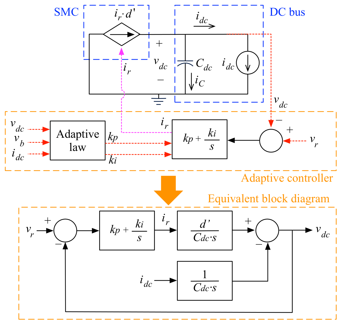
From the electrical scheme of Figure 1 it is observed that the average current in the MOSFET Q 2 is equal to d · i L . Then, taking into account that the SMC ensures i L = i r , the SMC, inductor, and Q 2 can be represented by a current source i r · d , as depicted in Figure 2. Such an equivalent closed-loop system also describes the internal structure of the adaptive controller, which generates the parameters k p and k i of the PI voltage controller using an adaptive law. Finally, the adaptive controller produces the reference i r for the SMC.
The block diagram of the equivalent closed-loop system is reported at the bottom of Figure 2, which describes the contributions of the reference and load currents into the DC bus voltage. From the equivalent block diagram, two transfer functions are calculated: G v d c , i d c , which describes the response of the bus voltage v d c to perturbations on the bus current i d c ; and G i r , i d c , which describes the response of the reference current i r to the same perturbations ( i d c ). Those transfer functions are first calculated in terms of the PI parameters k p and k i , but the denominators are in terms of the duty cycle; thus, the poles change with the operation conditions. Therefore, k p and k i must be adapted to ensure the same behavior in all the operation conditions. This is addressed by normalizing those parameters with respect to the duty cycle, producing the constant control parameters k p a = k p · d and k i a = k i · d ; thus, the adaptive law that must be processed in real-time is given in (13). Finally, the second forms of G v d c , i d c and G i r , i d c have constant poles:
G v d c , i d c = s C d c s 2 + k p · d C d c · s + k i · d C d c = s C d c s 2 + k p a C d c · s + k i a C d c
G i r , i d c = k p · d C d c · s + k i · d C d c s 2 + k p · d C d c · s + k i · d C d c = 1 d · k p a C d c · s + k i a C d c s 2 + k p a C d c · s + k i a C d c
k p = k p a d , k i = k i a d
Comparing the denominator of the previous transfer functions with the canonical characteristic equation s 2 + 2 · ρ · ω n · s + ω n 2 leads to the natural frequency expression ω n = K i a C d c and damping ratio expression ρ = k p a 2 · k i a · C d c . The damping ratio is defined as ρ = 1 to ensure a voltage response without oscillations, which requires the following k i a value:
k i a = k p a 2 4 · C d c
Moreover, the worst-case scenario corresponds to a step-current perturbation in the DC bus i d c = Δ i d c s , where Δ i d c is the step amplitude. Then, calculating the inverse Laplace transformation of v d c = G v d c , i d c · Δ i d c s produces the time-domain expression given in (15), and its time derivative is given in (16):
v d c = Δ i d c C d c · t · e k p a · t 2 · C d c
d v d c d t = Δ i d c C d c · 1 k p a · t 2 · C d c · e k p a · t 2 · C d c
The maximum deviation (overshoot, M O ) in the DC bus voltage occurs when the derivative (16) is equal to zero, which occurs at t M O = 2 · C d c k p a . Replacing such a time into (15) leads to the following k p a value, which ensures the desired M O :
k p a = 2 · Δ i d c · e 1 M O
The settling time for a ϵ band is calculated in (18) by solving (15) for v d c = v r ϵ · M O and t = t s , where W 1 · is the lower branch of the Lambert-W function.
t s = 2 · C d c · W 1 ϵ · M O · k p a 2 · Δ i d c k p a
Finally, during the operation of this adaptive controller, the adaptive parameters k p and k i must be calculated in real-time using (13), thus requiring i d c to calculate the complementary duty cycle d using (3). Therefore, this adaptive law requires the measurement of the DC-bus current i d c , as illustrated in both the circuit scheme of Figure 1 and block diagram of Figure 2.

4.1. Cdc Value for Global Stability

The SMC requires fulfilling the dynamic restrictions (10) to ensure global stability; thus, the dynamic behavior of i r must be analyzed. Calculating the inverse Laplace transformation of i r = G i r , i d c · Δ i d c s produces the time-domain expression given in (19), and its time derivative is given in (20):
i r = Δ i d c d · 1 e k p a · t 2 · C d c + k p a · t 2 · C d c · e k p a · t 2 · C d c
d i r d t = Δ i d c · k p a d · C d c · 1 k p a · t 4 · C d c · e k p a · t 2 · C d c
The maximum value of d i r d t occurs at t i r = 0 , producing max d i r d t = Δ i d c · k p a d · C d c . Then, replacing such a maximum value into restrictions (10) leads to the following C d c range to ensure global stability, which considers charge and discharge states:
C d c > max Δ i d c · k p a · L v d c v b · d i d c · R i , Δ i d c · k p a · L v b · d i d c · R i

4.2. L Value to Limit the Battery Current Derivative

The previous C d c range ensures that the dynamic restrictions (10) are always fulfilled, thus the reference current for the SMC ( i r ) is always limited by the instantaneous inductor current derivatives defined in the switched model (1).
However, since the battery current is imposed by the inductor current ( i b = i L ), the instantaneous maximum derivative in the battery current d i b d t is defined by the maximum inductor current derivatives described in (1) for u = 1 and u = 0 conditions. Then, the maximum battery current derivative is limited by calculating the inductance L from (1) taking into account the charge balance principle ( i d c = i L · d ): any L value higher than (22) ensures that the battery current derivative, in any condition, is always lower than the maximum limit max d i b d t used in (22) to calculate L, i.e., d i b d t = d i L d t < max d i b d t .
L > max v b + i d c d · R i , v d c v b + i d c d · R i max d i b d t
Therefore, selecting L using (22) limits the battery current derivative at the power stage level. Hence, this limitation is applied despite the control system adopted, i.e., the adaptive SMC proposed in this work, or any other control strategy like traditional PID.

4.3. Switching Frequency Limitation and SMC Control Law

The theoretical SMC could reach infinite switching frequency near the steady-state condition S x = 0 , hence a common solution is to introduce a hysteresis band δ S x , + δ S x using a hysteresis comparator, where δ S x is the hysteresis width. Such a hysteresis band changes the sliding-surface to Q x = δ S x < S x < + δ S x , producing the following SMC control law:
u = 0 if S x + δ S x 1 if S x δ S x
Therefore, the switching frequency is defined by the hysteresis ripple δ S x of the switching function (5), which is equal to the subtraction of the ripples in i L and i r because the SMC ensures that the average value of S x is zero. The ripple in i L and v d c were calculated in (4) as δ i L and δ v d c . Then, the ripple in i r is produced by the PI controller processing δ v d c , resulting in k p a · δ v d c since the integral of δ v d c is equal to zero due to the charge balance principle. Therefore, δ S x = δ i L k p a · δ v d c , and using the ripple values in (4) leads to Equation (24), where the discharge state is the worst-case scenario.
δ S x = d 2 · max F s w v b + i d c d · R i L + k p a · i d c C d c
Then, the switching frequency imposed by the SMC changes depending on the operating conditions, and it is calculated from (24) as follows:
F s w = d 2 · δ S x v b i d c d · R i L k p a · i d c C d c
Finally, the minimum switching frequency is obtained from (25), as reported in Equation (26), which must be evaluated in the worst-case scenario: minimum duty cycle and maximum load current.
min F s w = min d 2 · δ S x v b max i d c 1 min d · R i L k p a · max i d c C d c

4.4. Synthesis of the Design Procedure

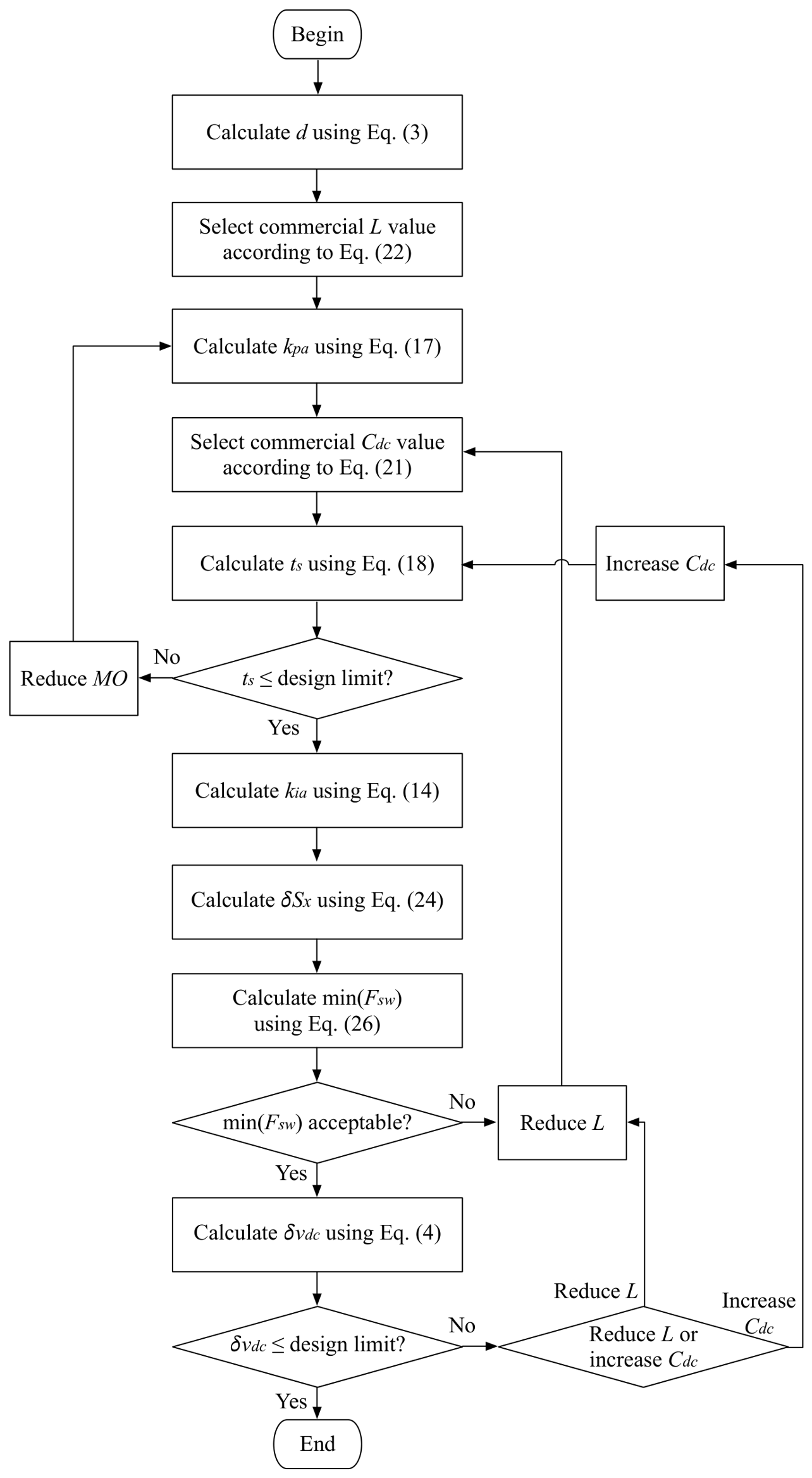
The design process starts by calculating the duty cycle d using (3), then a commercial inductance L is selected from (22). The next step is to calculate k p a using (17), and subsequently select a commercial capacitance C d c following (21). The settling time t s is calculated from (18). If such a value does not fulfill the application requirements (design limit), then M O must be reduced, which increases k p a to reduce t s . Then, k i a is calculated from (14), and the hysteresis band δ S x is calculated from (24).
The minimum switching frequency will not produce discontinuous conduction mode because the charger/discharger of Figure 1 is a synchronous converter, and the inductor current ripple is imposed by the SMC. However, low switching frequencies increase the voltage ripple δ v d c in the DC bus, as given in (4); therefore, Equations (4) and (26) must be used to verify that the maximum voltage ripple in the DC bus is acceptable (design limit). In addition, switching frequencies below 20 kHz produce audible noise; thus, Equation (26) must be used to verify that the selected value of L produces F s w 20 kHz. In this way, the design procedure considers reducing L if the minimum switching frequency is not acceptable. Moreover, if the voltage ripple δ v d c in the DC bus is not acceptable (higher than a design limit), L could be reduced to increase the switching frequency, or C d c could be increased as reported in (4).
Finally, Figure 3 summarizes the proposed co-design procedure for the power stage and control system of the battery charger/discharger.

5. Design Example and Experimental Validation

The proposed solution has been validated using a 24 V D C bus with a nominal current of 1 A and dynamic variations of 100 % of the load current. The choice of this application environment was guided by a combination of criteria: technological relevance, experimental feasibility, and the scalability of the prototype system, in line with the capabilities of the Electronics and Renewable Energy Laboratory of the Instituto Tecnológico Metropolitano, where the proof of concept was carried out.
The 24 V D C level is a well-established standard in multiple distributed energy and stand-alone system applications, superior to the typical 12 V in terms of transmission efficiency and compatibility with modern loads, but still accessible for academic prototyping. Its most relevant uses include: small-scale hybrid photovoltaic systems (100–500 W), backup systems and rural telecommunications microgrids, which operate at 24 V to power radio equipment, sensors, and remote stations, light electric vehicles and mobile platforms using dual-voltage architectures ( 12 V for control electronics and 24 V for small actuators/motors), and emerging industry standards for DC microgrids in buildings, where 24 V and 48 V are levels recommended by the Emerge Alliance and IEC 60364-7-710 [57] for safe power supply to low-power loads (less than 250 W) in non-specialized environments. With a nominal current of 1 A at 24 V , the DC power is 24 W, while transients of ± 1 A allow the dynamic response of the converter, the stability of the control loop, and the management of demand peaks to be evaluated—common scenarios, for example, when connecting/disconnecting loads such as DC fans, small pumps, or communication modules with impulse start-up. This range is sufficiently demanding to validate control strategies without requiring high-power devices or extreme safety measures.
To facilitate validation testing, the laboratory has Taraz’s SPM-FB evaluation platform based on SiC MOSFETs. This rapid prototyping solution can be reconfigured to produce different topologies of typical power converters. The module features integrated current and voltage sensors, and drivers for SiC MOSFETs with configurable dead time, short-circuit protection, per-channel low-voltage lockout, and active Miller clamping to prevent false triggering during fast switching. The above dramatically reduces gate control circuit design time, minimizes critical layout, and improves prototype reliability—aspects that are especially relevant when the focus is on the control algorithm, not low-level power electronics. One disadvantage of the platform is that its transistors (G3R75MT12D) are designed for high-current, high-voltage applications, which means their turn-on and turn-off energies are high, significantly increasing switching losses.
Accordingly, the proposed system was validated using an FL1223GS battery with a nominal voltage of 12 V . The reference voltage is v r = 24 V , the maximum load current is i d c = 1 A , the maximum load perturbation is Δ i d c = 1 A , the maximum DC voltage deviation is set to 5% ( M O = 1.2 V ), and the settling time (2% band) must be lower than 5 ms. The ON-resistance of the MOSFETs is 75 m Ω , the parasitic resistance of the inductor is 67 m Ω , and the series resistance of the battery is 90 m Ω , which results in R i = 232 m Ω . Moreover, since a second-life battery is considered, the battery current derivative must be limited to max d i b d t = 50 A/ms. Finally, the maximum switching frequency is set to max F s w = 75 kHz.
Applying the design procedure reported in Section 4.4 results in an average duty cycle d = 0.52 and a minimum inductance of 249.67 μ H , selecting the commercial inductance 2318-V-RC1720 with L = 330 μ H . Then, k p a = 0.6454 A/V is calculated. The minimum capacitance of 46.25 μ F is obtained by selecting C d c = 253 μ F , which yields a settling time t s = 4.5 ms, thus fulfilling the design requirement. Finally, k i a = 411.61 A/(V·s) and δ S x = 0.145 A are calculated.
This power stage serves as a scalable validation platform where modulation strategies, control, and protections tested at 24 V/1 A can be directly replicated in 24 V/5 A or 48 V/10 A systems by resizing passive and semiconductor components, without modifying the control logic or system architecture. This reinforces the transferability of results from the laboratory to other practical applications. Appendix A reports additional design examples validated with detailed circuital simulations, which consider high current and a wide range of voltage conversion ratios.

5.1. Circuital Simulations

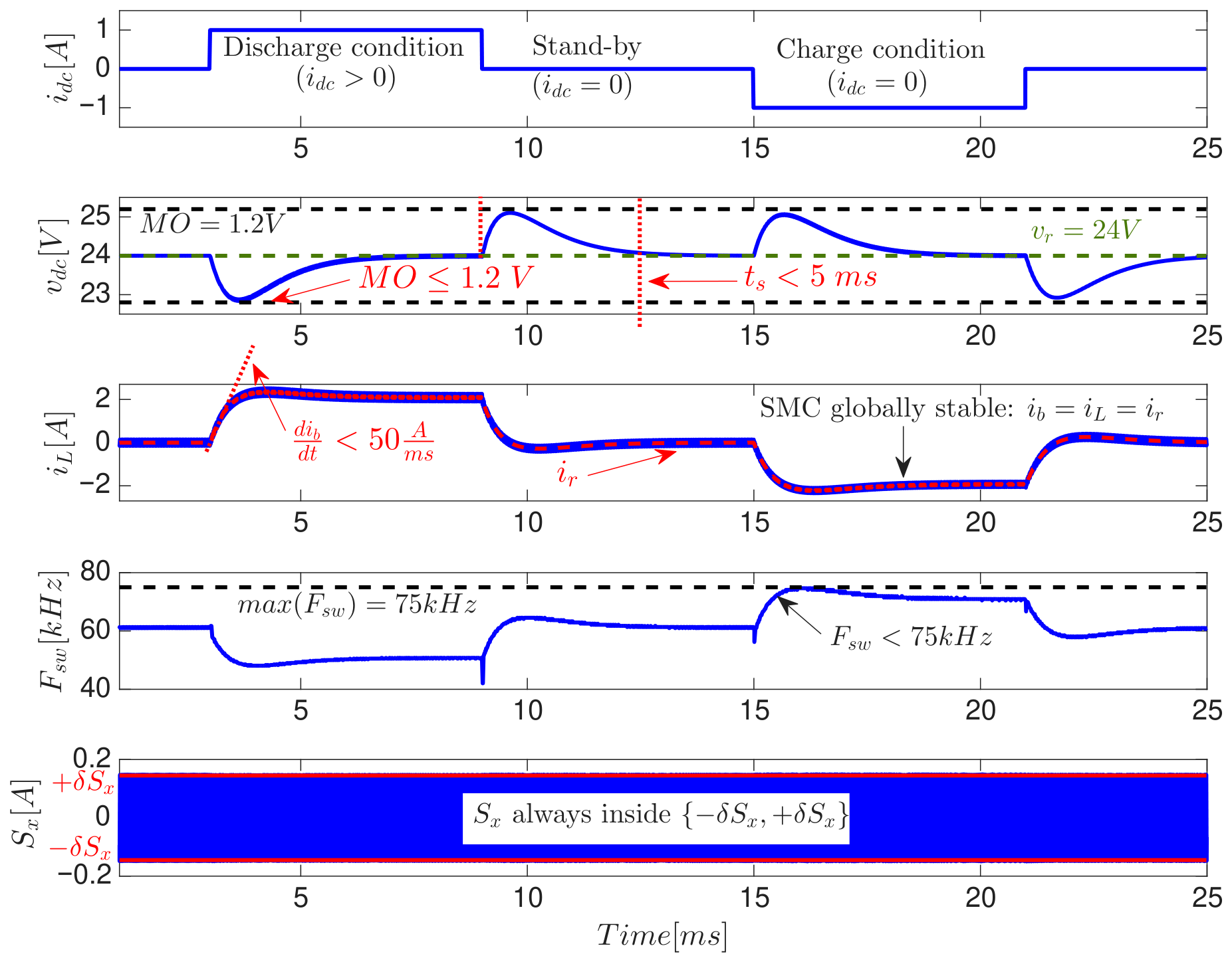
The power system of Figure 1 was implemented in the electronics simulator PSIM, including the designed SMC and adaptive controllers. Figure 4 reports the detailed simulation of the circuit and control systems, where the load profile considers discharge ( i d c > 0 ), charge ( i d c < 0 ), and stand-by ( i d c = 0 ) conditions. The perturbations in the DC bus current have step-like waveforms with 1 A amplitudes, thus producing deviations in the DC bus voltage. However, the cooperative action of the SMC and adaptive controllers imposes the desired behavior on the DC bus: the voltage is regulated at 24 V with maximum deviation M O 1.2 V and settling time t s < 5 ms. In addition, the correct operation of the SMC is observed, which also constrains the battery current derivative to the desired value d i b d t < 50 A/ms. The switching frequency is also limited to the desired range F s w < 75 kHz, and the switching function is always trapped inside the practical surface δ S x , + δ S x , which ensures the global stability. Moreover, the additional design examples presented in Appendix A confirm the correct results provided by the co-design procedure in a wide range of voltage conversion ratios and load currents.
It is worth noting that the circuital simulation of Figure 4 starts with the DC-bus capacitor already pre-charged at nominal voltage ( 24 V ). This is a common practice since battery chargers/discharges based on boost converters use well-known pre-charge circuits to avoid high inrush currents that could damage the battery and the power converter [58,59]. Appendix B discusses a classical start-up solution for DC-buses based on boost converters.

5.1.1. Performance Under Parametric Variations

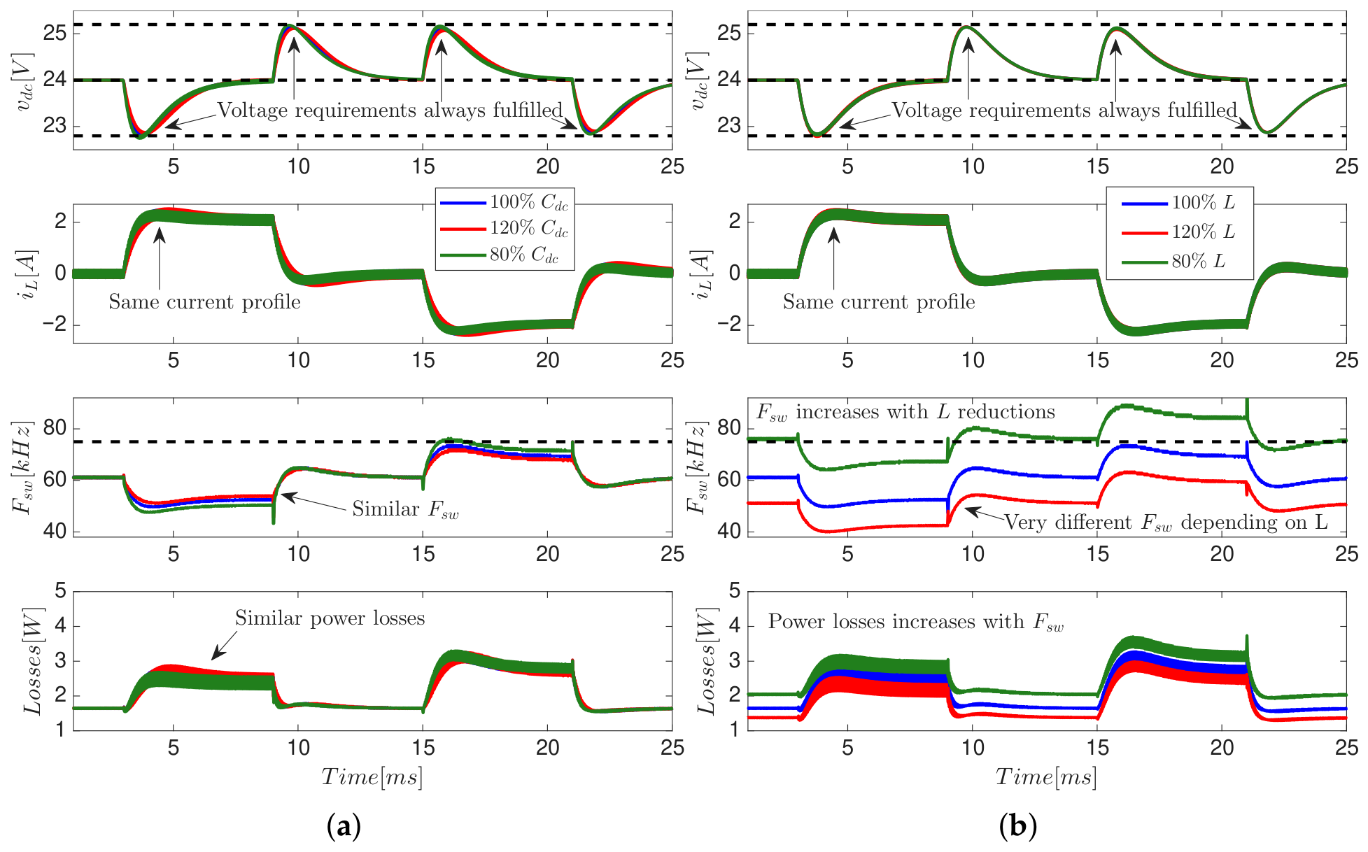
Six additional simulations were conducted to evaluate the robustness of the adaptive controller, which consider changes in the bus capacitance ( C d c ) and inductor (L). Those circuital simulations assume modifications of ±2% in both elements to be in agreement with maximum tolerances on commercial elements. Figure 5a shows that changes on C d c do not affect the DC bus voltage performance, fulfilling both M O and t s requirements. Similarly, the inductor current profiles are almost the same in the three cases. Both the correct bus voltage and the battery (inductor) current are produced by the adaptive capability of the proposed control system. The switching frequency imposed in the three cases of Figure 5a is very similar, where increments in C d c reduce the effect of i d c on F s w as it is observed in (25). The conduction losses P L o s s , Ω , which include the losses on the ON-resistance of the MOSFETs, the parasitic resistance of the inductor, and the series resistance of the battery, are calculated as given in (27). In addition, the switching losses are calculated from the switching frequency F s w , the MOSFETs’ turn-ON switching energy E o n , and the MOSFETs’ turn-OFF switching energy E o f f using the classical expression (28) reported in [60]. Finally, the total power losses P L o s s are given in (29). Given that the manufacturer of the G3R75MT12D transistors [61], considered in both simulations and experiments, reports an E o n = 217 μ J and E o f f = 52 μ J under conditions of 800 V / 20 A , scaling to the operating point of this application, 24 V / 2 A (inductor current), the turn-on and turn-off energies considered to calculate the switching losses are 21.7 μ J and 5.2 μ J , respectively. The bottom traces of Figure 5a show the power losses produced by the Adaptive SMC for the three C d c values. Those results show that the consistent F s w behavior also produces a consistent loss condition:
P L o s s , Ω = i L 2 · R i
P L o s s , s w = F s w · E o n + E o f f
P L o s s = P L o s s , Ω + P L o s s , s w
Figure 5b shows the performance of the Adaptive SMC to changes on L, where no effect on the DC bus voltage performance is present, thus fulfilling both M O and t s requirements. The same behavior is observed in the inductor (battery) current for all the values of L. Such consistent performance is achieved by the correct operation of the sliding-mode controller, which absorbs those changes in L into the switching frequency. In fact, the switching frequencies reported in Figure 5b increase with reductions on L, which is in agreement with expression (25). Since the switching power losses (28) are proportional to the switching frequency, the total power losses (29) are increased when L is decreased. Finally, it is evident that higher inductor values could improve the converter’s efficiency but at the expense of higher size and cost.
In conclusion, the simulations reported in Figure 5 confirm the correct DC bus voltage regulation even for 20% changes on both C d c and L. However, it must be noted that reductions in L increase the maximum switching frequency; thus, the solution design must include a safe margin for L to account for construction tolerances. Finally, the selected value L = 330 μ H ensures a minimum switching frequency of 52 kHz with a voltage ripple of 20 mV, and even with a tolerance of 20%, the minimum switching frequency is 42 kHz with a voltage ripple of 24 mV. Both minimum switching frequencies are acceptable for this example since those values are out of the audible range, and both DC voltage ripples are lower than or equal to 0.1%, which is very small.

5.1.2. Comparison with a Classical Solution

A classical solution based on PI structures is designed to provide an additional evaluation of the proposed approach. In this way, a small-signal model X ˙ = A m · X + B m · U is obtained using the state X and input U vectors reported in (30), which leads to the system matrices given in (31).
X = i L v d c U = d v b i d c
A m = R i L d L d C d c 0 B m = v d c L 1 L 0 i L C d c 0 1 C d c
The state-space system is completed with the output equation Y = C m · X + D m · U . The first option is to design a direct PI controller, which requires a transfer function of the bus voltage v d c with respect to the duty cycle d; such a transfer function is obtained using the matrices C m = 0 1 and D m = 0 0 0 as given in (32), which has a right half-plane (RHP) zero that makes difficult a direct control with a PI structure.
v d c ( s ) d ( s ) = 8237 · ( s 1.604 × 10 4 ) s 2 + 703 · s + 2.758 × 10 6
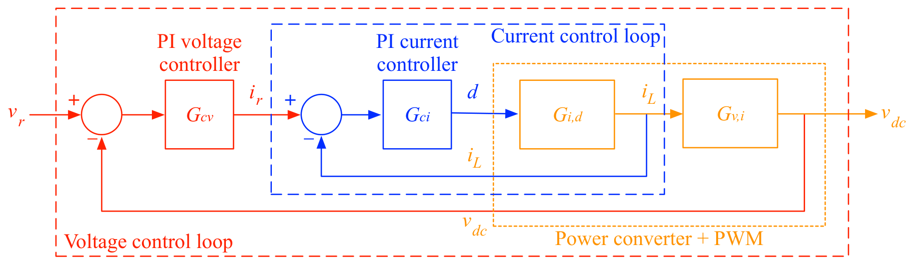
The classical approach for this kind of converter with RHP zeros is to control another state to produce a reduced-order model. Then, the transfer function of the inductor current i L with respect to the duty cycle d is obtained using the matrices C m = 1 0 and D m = 0 0 0 as given in (33), which can be directly controlled with a PI structure (no RHP zero present). The PI current controller G c i , given in (34), was designed from the transfer function (33) to provide the same performance of the proposed Adaptive SMC, i.e., a unitary damping ratio ( ρ = 1 ) and the fastest response possible. To provide a fair comparison with the Adaptive SMC, the PI control system includes a pulse-width modulator (PWM) with a switching frequency equal to max F s w = 75 kHz to ensure a comparable dynamic response. Finally, the controller G c i was designed with a closed-loop bandwidth equal to 1/10 of the switching frequency (7.5 kHz), which is a classical approach used to ensure stability [62]. Figure 6 shows the block diagram of the complete cascade control system based on PI controllers, where the orange blocks represent the power converter and PWM circuit; that model includes G i , d transfer function (33) between i L and d, and G v , i transfer function (35) between v d c and i L . Moreover, Figure 6 describes the current control loop (blue blocks) corresponding to the G c i PI controller (34), which regulates i L according to the reference i r . It is observed that G c i produces the duty cycle d for the PWM circuit.
G i , d = i L ( s ) d ( s ) = 72727 · ( s + 164.7 ) s 2 + 703 · s + 2.758 × 10 6
G c i = 0.53138 · ( s + 9863 ) s
Then, the average current of the Q 2 MOSFET (within a switching period) in the power converter of Figure 1 is i L · d , thus the reduced-order transfer function G v , i between the bus voltage and inductor current is given in (35). Finally, the cascade voltage controller G c v , given in (36), was designed using G v , i to avoid oscillations in the DC bus (unitary damping ratio, ρ = 1 ) with the fastest response possible; in this case, the safe bandwidth is equal to 1/10 of the inner (current) controller bandwidth as reported in [63], i.e., 0.75 kHz. Figure 6 describes this cascade voltage control loop (red blocks) corresponding to the G c v PI controller (36), which regulates v d c according to the reference v r . It is observed that G c v produces the reference i r for the current control loop.
G v , i = v d c ( s ) i L ( s ) = d C d c · s
G c v = 1.3503 · ( s + 640.2 ) s
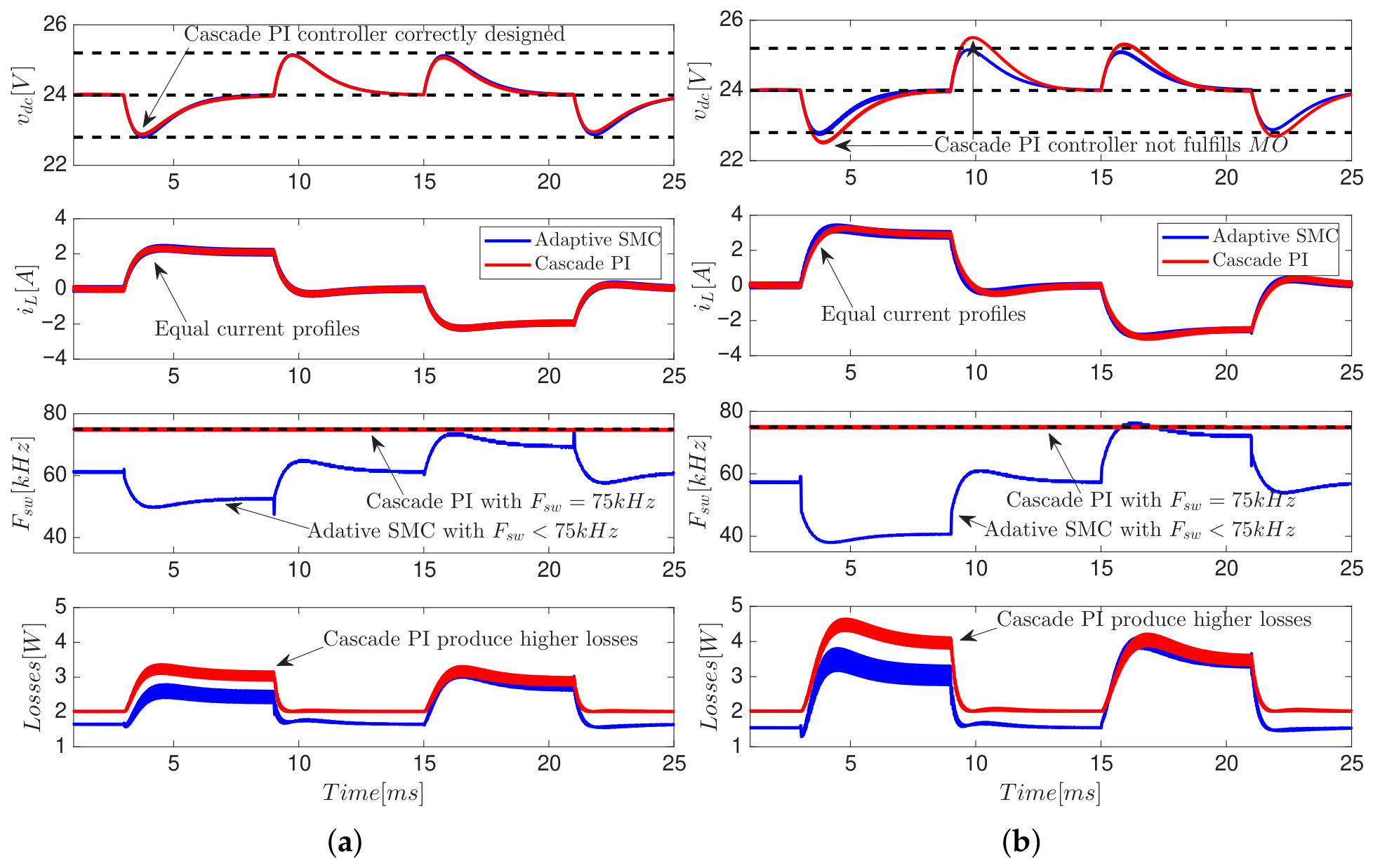
Figure 7a shows the performance of both Adaptive SMC (blue waveforms) and cascade PI controller (red waveforms) at the nominal battery voltage ( v b = 12 V ) used to design both approaches. These results demonstrate the correct design of the classical approach formed by G c i and G c v cascade controllers, where the PI solution achieves the same bus voltage and inductor current performance in comparison with the Adaptive SMC; i.e., both M O and t s are fulfilled. However, the cascade PI solution exhibits a constant switching frequency imposed by the PWM (75 kHz), thus the calculated power losses are higher than in the Adaptive SMC case.
The operation of any charger/discharger produces changes in the battery SoC, which affects the battery voltage ( v b ). Therefore, Figure 7b reports the circuital simulations of both solutions under a 25% reduction on v b to test the robustness of the controllers to changes in SoC. Those results show that the Adaptive SMC correctly regulates the bus voltage, fulfilling M O and t s to ensure a safe operation of the DC bus. This is achieved by the adaptive law of this solution (13), which modifies the controller to ensure the desired performance under any duty cycle condition, thus adjusting the controller to changes in the battery voltage. Instead, the circuital simulations of Figure 7b shows that the classical PI solution is unable to ensure the desired performance ( M O ) of the DC bus voltage under changes of the battery voltage, which puts at risk any source or load connected to the bus. This is a result of operating far from the condition used to design the PI controllers (nominal v b ), thus demonstrating the lack of robustness of this classical solution to changes in real operation conditions. In addition, similar to the operation at nominal v b , the switching frequency of the cascade PI is constant (75 kHz), and the power losses are higher than in the Adaptive SMC.
In conclusion, a classical solution based on PI structures can be designed to provide the same performance as the Adaptive SMC at some operation point, but changes in the operation conditions are not compensated by the PI controllers due to the lack of robustness, which leads to unsafe bus voltage performances that could damage the devices connected to the bus. Instead, the proposed Adaptive SMC provides the same desired performance under any operating condition, thus ensuring the safe operation of the bus and all connected devices. In addition, the Adaptive SMC ensures a maximum switching frequency imposed by (25) and a minimum switching frequency reported in (26), which, in this example, produces lower power losses in comparison with the classical solution.

5.1.3. Response to Current Pulses

The design of the capacitor C d c previously described in Section 4.4 considers step changes in the bus current i d c , which corresponds to a non-linear load because the impedance Z L changes when the bus voltage v d c has dynamic transients, i.e., Z L = v d c / i d c is not constant. However, some loads may exhibit high-current pulses, which the proposed system can regulate based on pulse characteristics.
A load current pulse can be described by two parameters: the pulse duration T p and amplitude I p . Since the pulse is usually very fast, all the pulse current is provided by the C d c capacitor; thus, the charge Q p extracted from C d c during the current pulse is Q p = T p · I p . Such a charge extraction from C d c produces a voltage reduction V p = Q p / C d c . On the other hand, when the bus voltage is reduced to the maximum deviation defined by M O , the capacitor C d c loses a charge Q M O = C d c · M O . Then, any current pulse with Q p Q M O will be compensated by the proposed system. Inequality (37) formalizes the acceptable relation between I p and T p for a load current pulse; if such a relation is not fulfilled, then C d c must be increased, otherwise the pulse will not be correctly compensated.
T p · I p C d c · M O
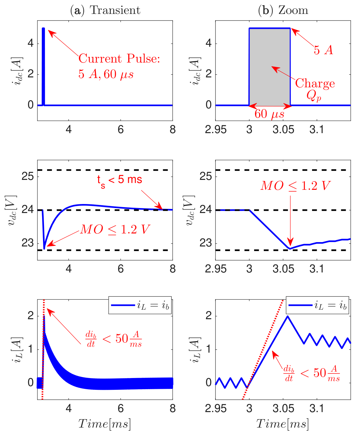
In the design example of this section Q M O = C d c · M O = 253 μ F · 1.2 V = 303.6 μ C . A load current pulse with 500% amplitude with respect to the nominal value of 1 A ( I p = 5 A ) and a duration of T p = 60 μ s will impose a charge extraction of 300 μ C , thus fulfilling restriction (37). Therefore, such a load current pulse with 500% amplitude will be correctly regulated. This is tested in the circuital simulation reported in Figure 8, which considers the 500% current pulse ( 5 A ) with 60 μ s duration.
Figure 8a shows the application of the 5 A current pulse in i d c at 3 ms, where the DC bus voltage is correctly constrained to M O 1.2 V , i.e., v d c 22.8 V . Similarly, since the battery current is imposed by the inductor current ( i L = i b ), the derivative of the battery current is limited following (22), which in this design example must fulfill d i b d t < 50 A/ms. Finally, it is observed that the desired settling time is achieved, i.e., t s < 5 ms. Figure 8b shows a zoom between 2.95 ms and 3.15 ms, where the detail of the load current pulse in i d c is observed. Moreover, the zoom in Figure 8b shows the detail of the bus voltage v d c waveform, where the voltage drop produced by the charge Q p extraction is evident. Since Q p < Q M O , then the bus voltage deviation is lower than the design limit, i.e., M O 1.2 V . Finally, the bottom traces of Figure 8b confirm that d i b d t < 50 A/ms even under a very large (500%) load current pulse.
In conclusion, any current pulse produced by the load that fulfills restriction (37) is correctly compensated. However, the C d c capacitor must have sufficient current rating; otherwise, it will be damaged.

5.2. Experimental Results

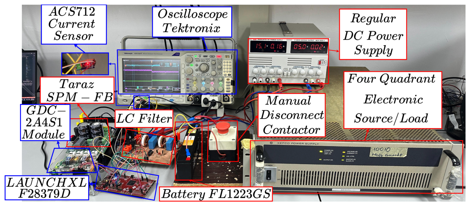
The proof-of-concept of the proposed solution was implemented in a laboratory environment, as shown in Figure 9. The bidirectional buck-boost converter was developed with a branch of Taraz’s SPM-FB full bridge using G3R75MT12D transistors (Global Power Synergies, Lake Forest, USA) and the series connection of two 43ML5M capacitors (Rubycon Corporation, Ina, Japan) making C d c = 253 μ F , the LC filter consists of the inductor L = 330 μ H and a capacitor 22 μ F connected in parallel with the battery. For safety reasons, a manual switch allows the battery to be disconnected. The Kepco BOP-5020GL ( Kepco Inc., New York City, USA) four-quadrant source/load was used to emulate DC bus operation, enabling programming of current changes on the DC bus. The control strategy was implemented using the TI LAUNCHXL-F28379D development board (Texas Instruments, Dallas, USA), which produces the switching functions for the Taraz GDC-2A4S1 drivers (Taraz Technologies, Islamabad, Pakistan), with dead time configured to 0.64 μ s because its adjustable range is 0.39579 μ s to 8.3 μ s . Voltage dividers with the OPA484 in follower mode enable the sensing of DC bus and battery voltages. The AD8210 sensor (Analog Devices, Wilmington, USA) included in the LC Filter card measures the inductor current, and the ACS712 sensor (Allegro MicroSystems Inc., Manchester, USA) measures the i d c current. A Tektronix MDO3024 oscilloscope, TPP0500 voltage probes, and TCP0020 current probes (Tektronix Inc., Beaverton, USA) were used to verify the system’s operation. Finally, in the experimental set-up the Kepco BOP-5020GL four-quadrant source/load was used to pre-charge the DC-bus capacitor at nominal voltage ( 24 V ), which protects the battery from high start-up currents and avoids the construction of classical start-up circuits like the solution discussed in Appendix B.
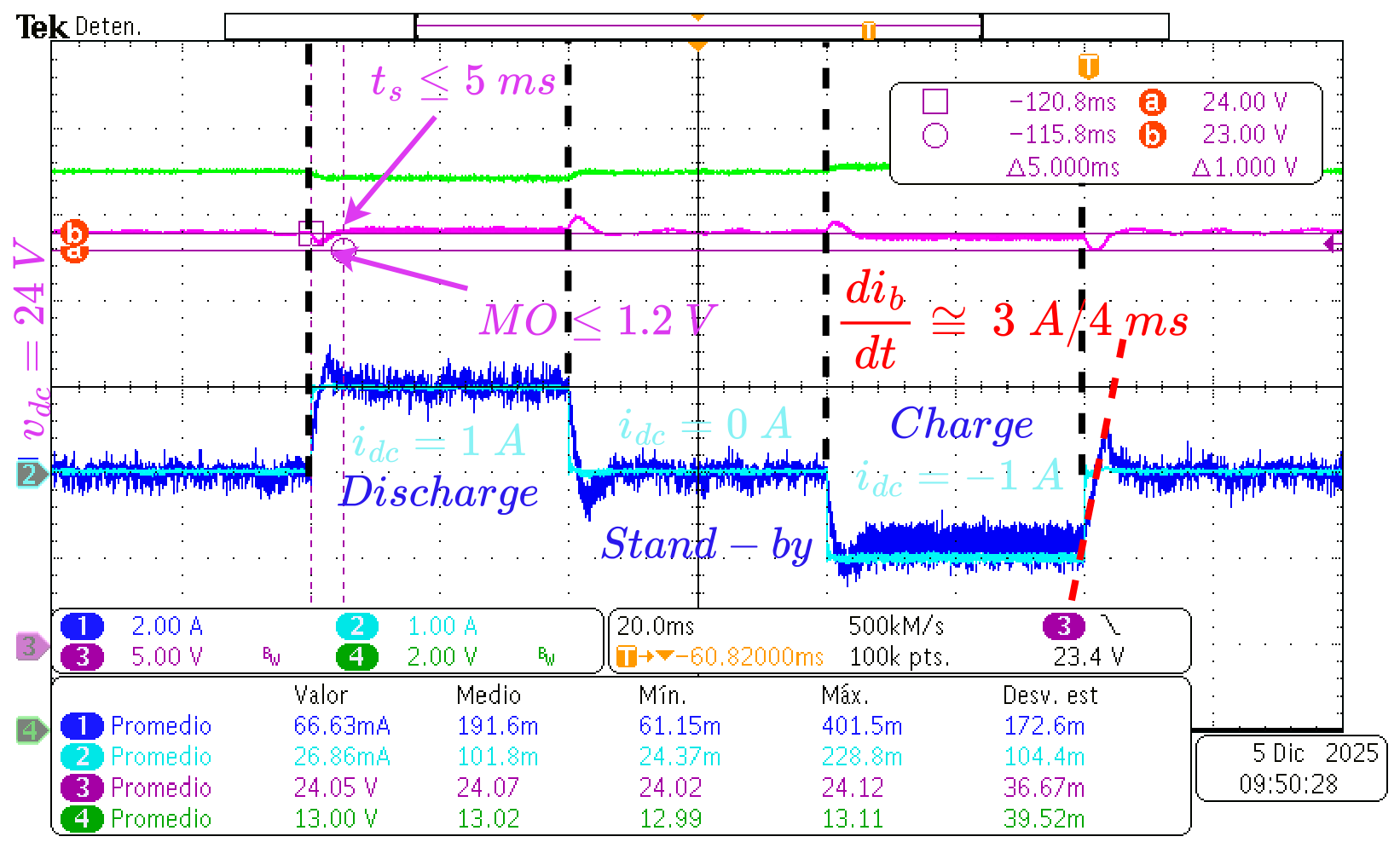
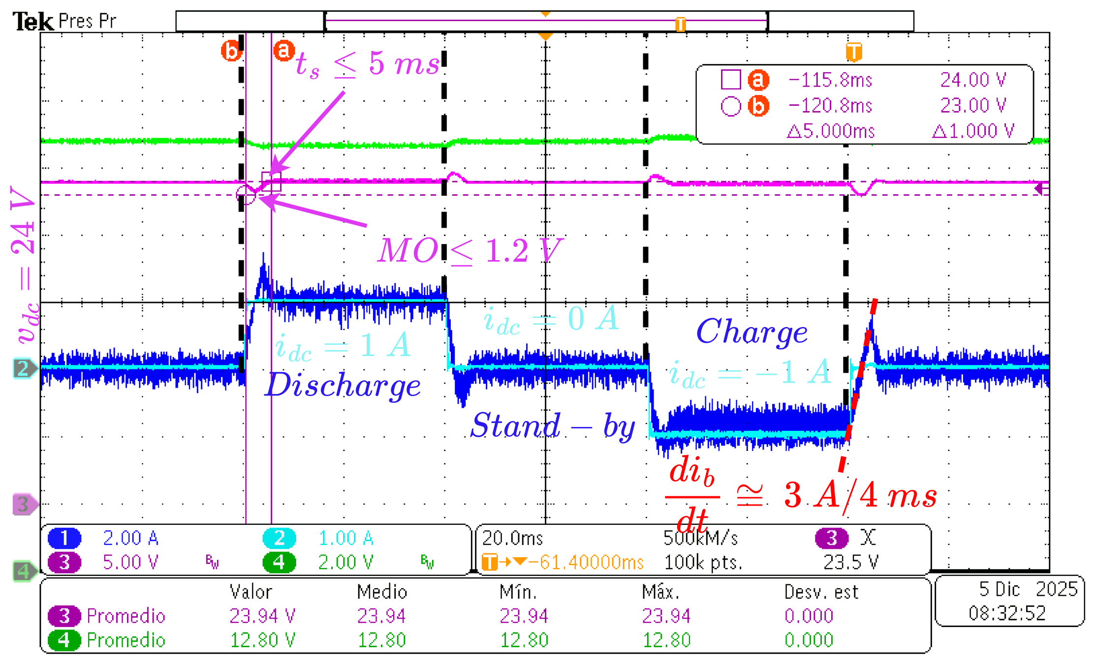
Figure 10 shows the experimental results for discharge, stand-by, and charge modes; the magenta line is the bus voltage, which remains at 24 V for all the operating conditions; the blue line is i L , and the light blue line is i d c . For discharge mode, i d c = 1 A produces i L 2.1 A, which is consistent with the boost converter operation because battery voltage is 12.8 V. In charging mode, i d c = −1 A produces i L −1.6 A with a 13.2 V battery voltage; these results show that the battery voltage varies with operating mode. In discharge mode, the battery voltage is lower than its nominal value, resulting in higher gain voltage and current, i.e., a higher inductor current than in charge and stand-by modes. As the figure shows, after a step-like DC bus current change, inductor current changes with a slope of 0.75 A/ms, fulfilling the design restrictions, and the DC bus voltage shows a transient behavior with M O 1.2 V and t s 5 ms, which is in agreement with the design procedure and simulation results.
To evaluate the robustness of the adaptive controller, adding a 220 μ F capacitor in parallel with the DC bus capacitance ( C d c ) allows emulating changes in the charger/discharger parameters. Figure 11 shows results for discharge, stand-by, and charge modes with the additional 220 μ F capacitor; the bus voltage remains at 24 V across all operating conditions, with less oscillation in steady-state operation. For discharge mode, i d c = 1 A and i L 2.1 A for v b = 12.8 V; in charging mode, i d c = −1 A and i L −1.6 A with a 13.2 V battery voltage. The transient behavior is similar to the results in Figure 10, i.e., M O 1.2 V and t s 5 ms, fulfilling the design criteria and in agreement with simulation results in the Section 5.1.1. It is important to note that reducing C d c or changing the inductor value requires desoldering and soldering new components, which can affect the integrity of the Taraz bridge and the LC filter; therefore, no additional parametric changes were considered in the experimental case.
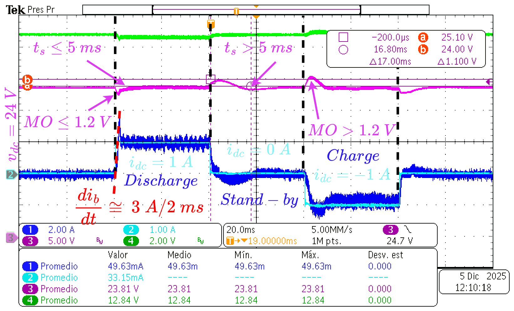
Another experimental test based on the classical cascade PI control strategy, designed in Section 5.1.2, provides an additional evaluation of the proposed approach. Figure 12 shows results for discharge, stand-by, and charge modes. For the discharging mode, the design criteria are fulfilled because M O 1.2 V and t s 5 ms, but the transition from discharging to stand-by shows a settling time higher than 5 ms. Also, from stand-by to charging mode M O > 1.2 V, these results show a proper regulation of the DC bus voltage at 24 V for the three operation modes. However, the transient behavior does not always meet the design criteria because the PI control is designed based on a small-signal model around the discharge operating point. Otherwise, the adaptive controller proposed in this work meets the design criteria at all operating points, as shown in Figure 10 and Figure 11.
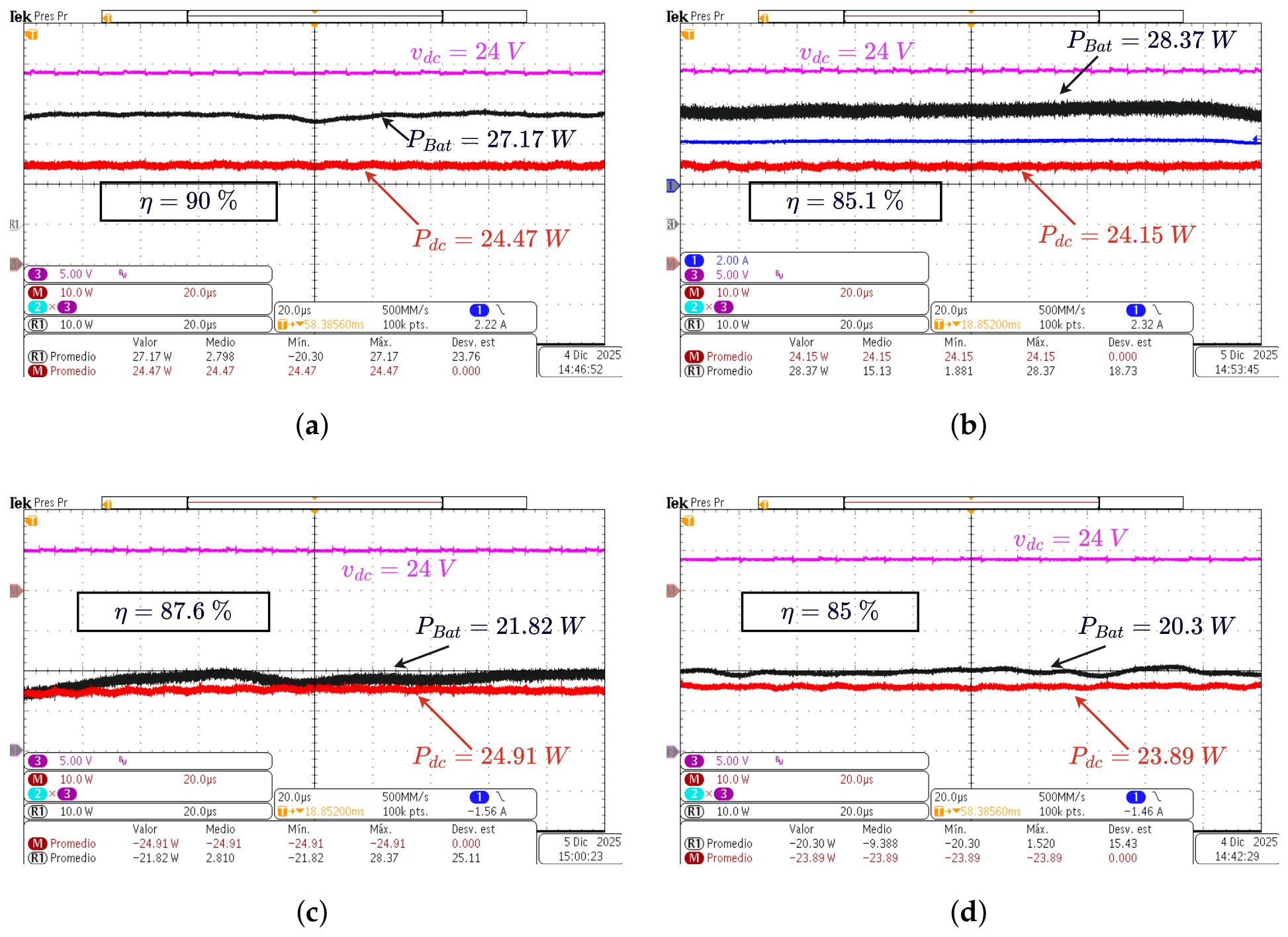
The adaptive SMC control strategy exhibits proper transient behavior at all operating points, whereas the PI control strategy does not, due to the linearization required for PI design. Additionally, power losses and efficiency highlight the advantage of the adaptive SMC strategy over the PI control. Figure 13 shows the battery power ( P B a t ) in black line and the power at the DC bus ( P d c ) in red line, while regulating v d c at 24 V in discharging and charging modes for the adaptive SMC control (Figure 13a,c) and PI control (Figure 13b,d). In discharging mode, the battery acts as a power source and the DC bus as a power load. Figure 13a shows 2.7 W power losses yielding 90% efficiency, while Figure 13b shows 4.22 W power losses yielding 85.1 % efficiency. In charging mode, the battery acts as a power load, and the DC bus as a power source; due to the change in the energy flow, the power measures show a negative sign. Figure 13c shows 3.09 W power losses yielding 87.6 % efficiency, while Figure 13d shows 3.59 W power losses yielding 85 % efficiency. Efficiency results demonstrate that the proposed adaptive SMC controller is a better option than the PI control strategy due to lower power losses. It is important to note that the dead time between switching signals was not accounted for in the efficiency analysis, as a fixed value of 0.64 μ s was set in accordance with the driver manufacturer’s recommendations and maintained throughout all tests; besides that dead time introduces a delay lower than 5.1 % for switching signals with frequency lower than 80 kHz, thus its effect is negligible.
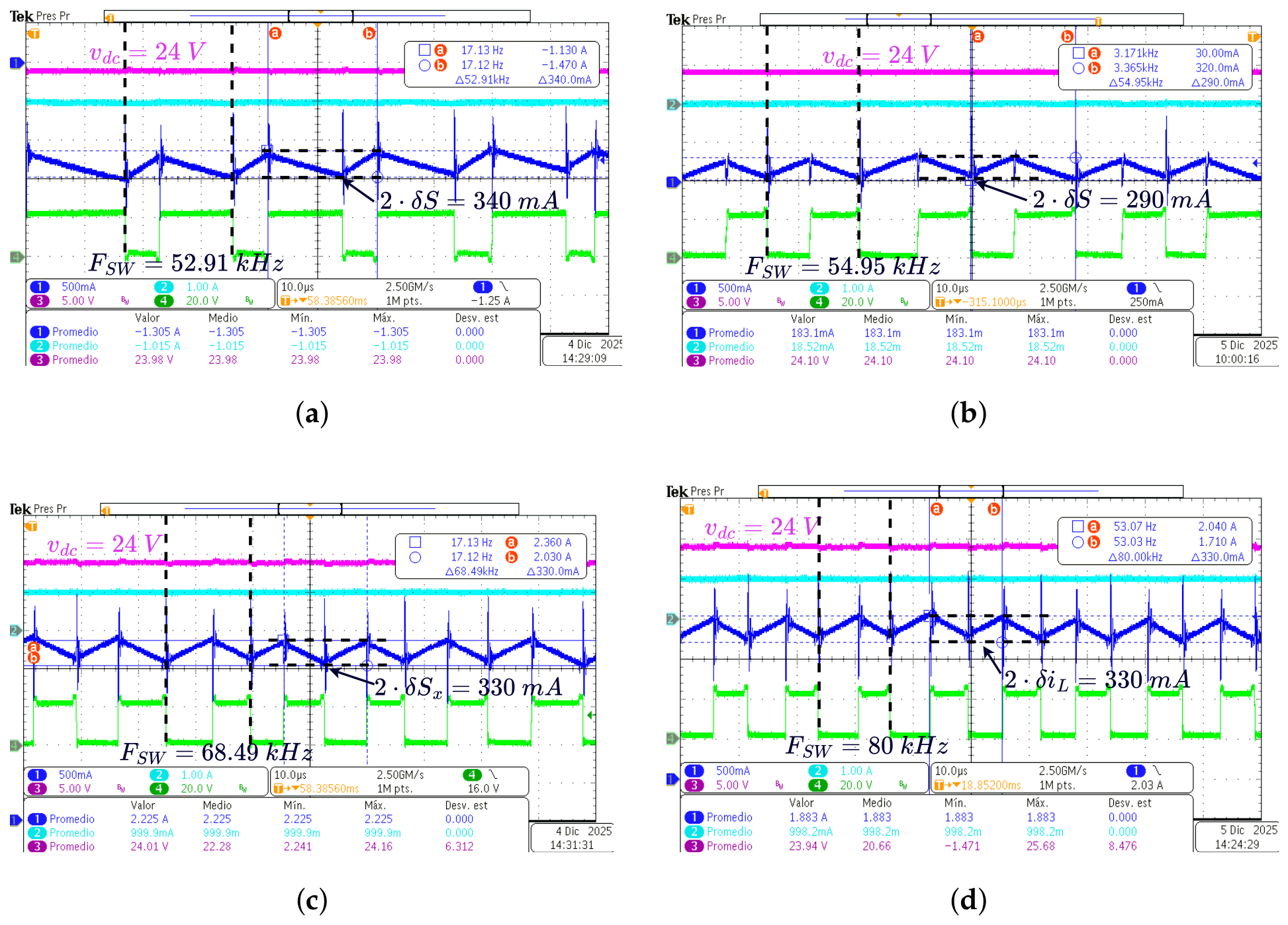
Power losses in power converters increase with higher switching frequency; in this sense, Figure 14 shows the steady-state inductor current in blue line and the switching signal in green line for charging (Figure 14a), stand-by (Figure 14b), and discharging (Figure 14c) modes concerning the adaptive SMC controller. Figure 14d shows the same variables in discharge mode for the PI controller; only discharge mode is shown because this strategy operates at a fixed frequency across all operating modes. Figure 14 highlights that inductor current ripple is between 290 mA and 340 mA for both control strategies and for all operating points, due to the hysteresis band in the adaptive SMC controller, and to the 80 kHz fixed frequency in the PI controller (see Figure 14d). The small variation in the inductor current ripple measured by the oscilloscope is caused by the current ringing occurring in the MOSFETs, but such a variation does not affect the system operation since the SMC is globally stable. For the adaptive SMC controller, the switching frequency is higher in discharge mode (68.49 kHz) than in charging (52.91 kHz) or stand-by (54.95 kHz) modes, because the battery voltage drops while battery discharge, causing an increase in the voltage and current gain, yielding an increase in the inductor current and switching frequency. Nevertheless, the switching frequency is lower with the adaptive SMC controller than with the PI controller for the same inductor current ripple, which explains the better efficiency of the control strategy proposed in this work.
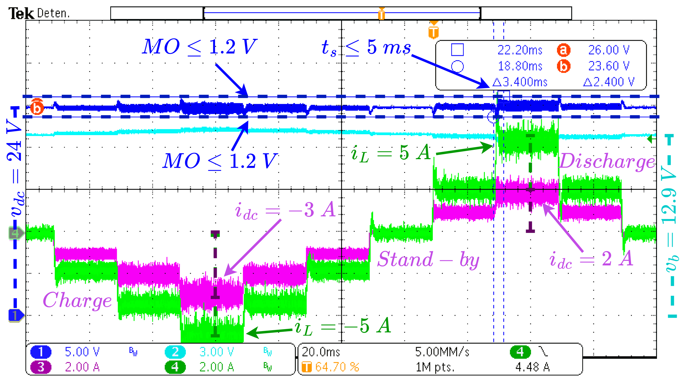
To demonstrate the flexibility of the charger/discharger system, Figure 15 shows an additional experiment with higher load power; thus, 1 A step changes in i d c allow evaluation of the system behavior. This test is limited to i L 5 A because that is the maximum average current supported by the commercial inductor 2318-V-RC172. In the charging scenario, i L reaches −5 A when i d c = −3 A showing 72 W of power on the DC bus due to v d c = 24 V, and 66 W of power on the battery due to v b = 13.2 V; for this operating point, the system reaches 91.6 % of efficiency. For discharging scenario, i L reaches 5 A when i d c = 2 A showing 48 W of power on the DC bus due to the regulated DC bus voltage, i.e., v d c = 24 V; also the system shows 63 W of battery power due to v b = 12.6 V; for this operating point, the system reaches an efficiency of 76.2 % . It is important to highlight that for all current step changes, the DC Bus voltage reaches the reference value ( v d c = 24 V) with a settling time lower than 5 ms and a M O lower than 1.2 V. These results confirm the adaptability of the charger/discharger platform to a higher load power while fulfilling the design criteria.
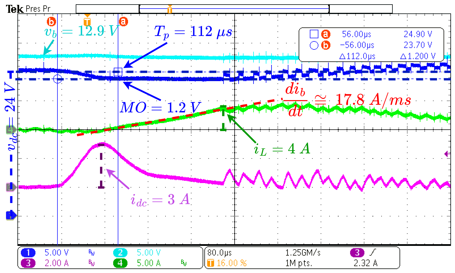
The system response to a high current pulse in the DC bus is reported in Figure 16, which shows the experiment with a temporal overload of 300 % , i.e., i d c = 3 A. It is important to highlight that the Kepco source/load used to program the current changes on the DC bus does not allow current pulses shorter than 100 μ s because of its rise time limit; therefore, the i d c pulse in Figure 16 is not a square pulse but reaches the desired peak amplitude. For the test, the system operates in a stand-by mode when the action of the i d c pulse causes v d c to decrease during 112 μ s without exceeding the expected 1.2 V voltage drop, i.e., M O = 1.2 V. In addition, the i d c pulse cause an increment in i L to compensate the voltage drop in v d c , therefore, the inductor current shows an slope of d i b d t 17.8 A/ms fulfilling the design criteria. After i d c returns to 0 A, inductor current shows the ripple caused by the switching operation required to regulate the DC bus voltage, and therefore v d c increases, showing a voltage ripple and causing a current ripple in i d c . These results agree with the analysis in Section 5.1.3 and with Equation (37), showing that even under critical current overload, the design criteria are fulfilled.
The experimental results demonstrate the feasibility of the proposed solution for charging and discharging second-life batteries, including its operating restrictions on the converter-controller design.

6. Conclusions and Future Works

A charger/discharger system based on a bidirectional boost converter with cascade control was proposed: Internal current control based on sliding modes and external voltage control based on an adaptive PI. The design of the power stage elements, inductor, and capacitor limits the derivative of the battery current and ensures the overall stability of the system. The system was validated through PSIM simulations and experimental tests for a 12 V battery and a 24 V DC bus in charge mode (−1 A), discharge mode (+1 A), and standby mode (0 A). The system strictly complies with performance constraints: A settling time of less than 5 ms and a maximum overshoot of 5%. In addition, the maximum switching frequency and the maximum rate of change of battery current derivative are limited, reducing degradation of second-life batteries. The results confirm the feasibility and effectiveness of the proposed approach, and a synthesized design procedure is presented that coherently integrates the control and power stages, facilitating its practical implementation in other types of battery chargers/dischargers.
Limiting the current derivative ( d i / d t ) in batteries is essential to preserve their electrochemical integrity and extend their service life. In new batteries, this limitation protects the solid–electrolyte interface (SEI) and prevents the formation of inactive metallic lithium, reducing capacity from the first cycle. In second-use batteries, whose internal resistance increases and capacity decreases, strict control of d i / d t is critical to avoid deep voltage drops, overheating, and cell imbalances. This limitation must be implemented in both the converter design (using inductive filters) and the controller, with the controller dynamically adjusting the limits based on the battery’s state of health.
Although the use of high-capacity SiC devices in very low-power applications results in significant efficiency losses, especially at high switching frequencies, the Taraz SPM-FB platform is highly suitable for proof-of-concept testing to validate functionality, stability, and control strategies. In fact, the proof-of-concept prototype developed in this paper achieved an efficiency of 90%. Nevertheless, future work will focus on designing a new prototype with components optimized for the precise current and voltage levels required by both the battery and the DC bus, thereby improving overall efficiency and reducing system cost.
This work also shows an interesting comparison between fixed and variable switching frequency in power converters. Control systems with variable switching frequency introduces some disadvantages with respect to fixed-frequency control techniques: (i) the passive elements of the converter must be designed for the lowest frequency to avoid high switching ripples; (ii) in variable frequency systems the switching losses could become very high if the switching frequency is not limited; and (iii) the variable frequency produces electromagnetic interference (EMI) in a wider frequency spectrum, while fixed-frequency techniques concentrate the EMI at the constant switching frequency; hence, it is easier to filter. However, this paper has adopted several techniques to mitigate (not avoid) those problems in the co-design of both the power stage and adaptive sliding-mode controller: (i) the co-design process considers an iterative design of the hysteresis band (23) and inductor (22) to impose the desired minimum switching frequency, thus avoiding very large passive elements. Moreover, (ii) the hysteresis width of the SMC (24) is calculated to limit the maximum switching frequency, also limiting the switching losses. This aspect was experimentally verified with the results reported in Figure 13, where the proposed adaptive SMC solution exhibits higher efficiency in comparison with a traditional PWM-based PI controller operating at fixed frequency. In addition, (iii) the combined limitation of both the minimum and maximum switching frequencies defines a predictable operational EMI frequency spectrum. This reduces the peak power of the EMI noise observed at the fixed frequency of traditional PWM solutions but requires wider (or adaptive) EMI filters. The design of those EMI filters is under investigation.
Other interesting aspects of SMC include its improved transient response, as the controller keeps the switching period active until the controlled variable reaches the desired value; however, this results in a variable switching frequency. In addition, the SMC could provide global stability and robustness to changes in converter parameters, but its design is much more complex than that of a classical PID controller. Moreover, despite the SMC having a very simple control law (23), its implementation requires precise analog comparators and custom circuits, whereas classical fixed-frequency controllers can be implemented with readily available integrated circuits. Those last two characteristics make the PID alternative much more common in industrial applications. Finally, this paper is aimed at simplifying the design of adaptive SMC approaches by providing an easy-to-follow co-design procedure for both the power stage and control system.
Considering the contributions of this work: integration of power and control stage design, current derivative limitation, robustness, and precise regulation, it is possible to propose future work addressing current challenges in energy storage, smart power electronics, and transport decarbonization.
A first task is to extend the integrated design methodology to hybrid storage systems (battery + supercapacitor), with a focus on dynamic power management and peak current mitigation. This work would explore the adaptation of the simultaneous converter-controller approach for hybrid systems, leveraging supercapacitors’ ability to absorb current transients while batteries operate in slow-current-change. The impact on the overall system lifetime and energy efficiency under real load profiles, such as those found in urban microgrids or electric transportation, would be evaluated.
Another possible task is the design of a smart converter with self-reconfiguration capabilities based on the battery’s state of health (SoH) and grid conditions. Building on the robustness and stability of the current system, it proposes incorporating online diagnostic algorithms and adaptive control strategies that dynamically adjust the d i / d t limits and the control loop dynamics in response to storage degradation. The above would preserve the quality of the DC bus and further extend the system’s operability in the face of aging or incipient failures.
The use of other control techniques in the integrated methodology is another possible area for future work. The overall methodology presented is based on regulating the inductor current to ensure global stability, using the sliding-mode technique. In addition, the power stage co-design is performed to ensure global stability across all operating conditions and safe DC-bus characteristics. This same approach can be applied to other control techniques, such as passivity-based current control. However, the equations for co-designing the power-stage parameters must be modified to reflect the new stability conditions. Therefore, it can be used to extend the co-design process by accounting for other globally stable control techniques more suited to particular applications, such as motor control or renewable generation systems.
Finally, this work could be extended to the implementation and experimental validation of the methodology in a bidirectional charger for electric vehicles, with integration into the smart grid (V2G/G2V) and compliance with harmonic injection and flicker regulations. This work would transfer the solution proposed in this article to the field of electric mobility, evaluating its performance under fast-charging, power injection into the grid, and supply-voltage fluctuations. It would focus on ensuring compliance with standards such as IEEE 1547 [64] and IEC 61000-3-12 [65] and on validating not only DC bus stability but also power quality at the common coupling point.

Author Contributions

Conceptualization, C.A.R.-P., E.E.H.-B. and S.I.S.-G.; methodology, C.A.R.-P. and E.E.H.-B.; software, C.A.R.-P. and S.I.S.-G.; validation, C.A.R.-P. and E.E.H.-B.; formal analysis, C.A.R.-P. and S.I.S.-G.; investigation, C.A.R.-P., E.E.H.-B. and S.I.S.-G.; resources, C.A.R.-P., E.E.H.-B. and S.I.S.-G.; data curation, C.A.R.-P. and E.E.H.-B.; writing—original draft preparation, C.A.R.-P., E.E.H.-B. and S.I.S.-G.; writing—review and editing, C.A.R.-P., E.E.H.-B. and S.I.S.-G.; visualization, C.A.R.-P., E.E.H.-B. and S.I.S.-G.; project administration, E.E.H.-B. and S.I.S.-G.; funding acquisition, E.E.H.-B. and S.I.S.-G. All authors have read and agreed to the published version of the manuscript.

Funding

This work is funded with resources from “Patrimonio Autónomo Fondo Nacional de Financiamiento para la Ciencia, la Tecnología y la Innovación, Francisco José de Caldas” under the call No. 938 from Minciencias, and it is carried out under the contract No. 112721-394-2023. The work reported in this paper is one of the results from the research project “Diseño de una plataforma de hardware/software para la caracterización y operación de sistemas de almacenamiento que incluyan baterías de segunda mano en microrredes eléctricas orientadas a zonas no-interconectadas de Colombia” (Minciencias code 105895), which belongs to the research program “TULATO—Tecnologías para la adopción de sistemas energéticos y de movilidad eficientes que fomentan el desarrollo sostenible orientados a regiones con alto potencial bio social y energético como Tumaco, Nariño” (Minciencias code 1150-938-100864). Finally, the writing of this paper was also supported by the Universidad Nacional de Colombia (HERMES code 59803) and Institución Universitaria ITM (code RC 112721-394-2023).

Data Availability Statement

The data generated in this work is reported in the manuscript.

Conflicts of Interest

The authors declare no conflicts of interest. The funders had no role in the design of the study; in the collection, analyses, or interpretation of data; in the writing of the manuscript; or in the decision to publish the results.

Appendix A. Additional Design Examples

In order to illustrate the versatility of the co-design process, this appendix presents additional design examples with different parameters. Those examples use the same power system (shown in Figure 1) implemented in PSIM, including the adaptive SMC controller. Therefore, only the passive component values, semiconductor rating, and controller parameters are updated without modifying the control logic or system architecture. This confirms the usability of the co-design procedure in a wide range of practical applications.

Appendix A.1. Higher Load Current

This first additional design uses the same DC bus and nominal battery voltages considered in the design example of Section 5 ( v b = 12 and v d c = 24 V ); moreover, the same maximum deviation of 5% ( 1.2 V ) and switching frequency (75 kHz) are adopted. However, the maximum load current is set to 5 A with a maximum settling time of 10 ms, and the maximum current derivative in the battery is considered as 100 A/ms.
Applying the design procedure reported in Section 4.4 results in an average duty cycle d = 0.63 at maximum current ( 5 A ) and a minimum inductance of 151.43 μ H , selecting the commercial inductor value L = 165 μ H . Then, k p a = 3.36 A/V is calculated. The minimum capacitance of 0.85 mF is obtained by selecting C d c = 2 mF, which yields a settling time t s = 8.1 ms, thus fulfilling the design requirement. Finally, k i a = 1412.4 A/(V·s) and δ S x = 0.29 A are calculated.
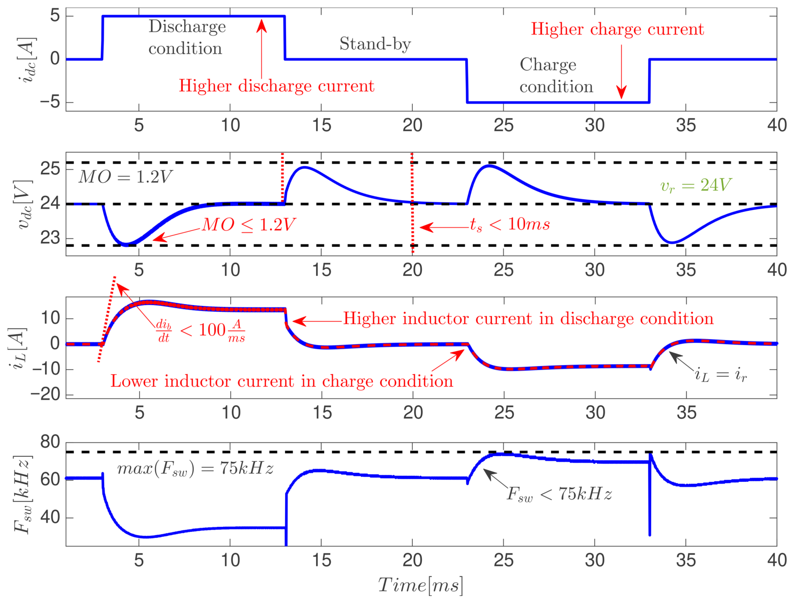
Figure A1 reports the detailed simulation of this new co-design, where the load profile considers discharge at i d c = 5 A , charge at i d c = 5 A , and stand-by ( i d c = 0 A ) conditions. The simulation confirms the correct bus regulation at 24 V with maximum deviation M O 1.2 V and settling time t s = 8.1 ms < 10 ms. Moreover, the battery current derivative is limited at the desired value d i b d t < 100 A/ms, and the switching frequency is limited to the desired range F s w < 75 kHz. This simulation was performed considering the same R b , R O N , and R L reported in Section 5, which forces the adaptive-SMC to impose a higher inductor current in discharge condition to compensate for the converter losses, reaching 13.5 A . Instead, in the in-charge condition, the adaptive-SMC does not require a high inductor current to regulate the DC bus voltage, only reaching 8.6 A . This example shows the stability of the control system over a wide range of inductor and load currents.
Figure A1. Circuital simulation of the battery charger/discharger for 24 V / 5 A .
Technologies 14 00257 g0a1

Appendix A.2. Higher DC Bus Voltage

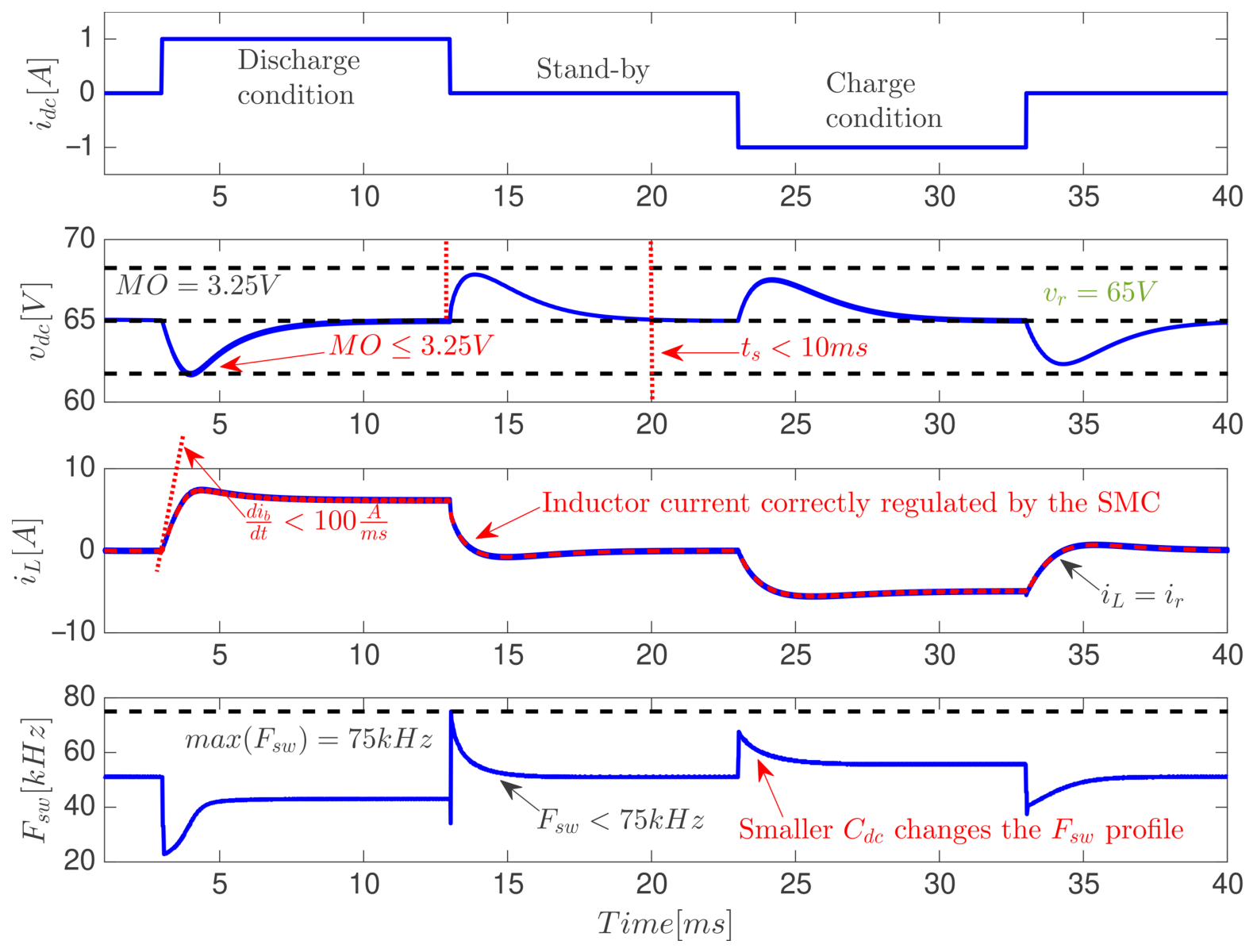
This second additional design considers a much higher DC bus voltage equal to 65 V , which is used to test system performance at high duty cycles. This application uses the same nominal battery voltage, switching frequency, maximum current derivative in the battery, and maximum settling time adopted in the previous design example Appendix A.1. Moreover, the maximum deviation of 5%, in this case, corresponds to M O = 3.25 V , and the maximum load current is set to 1 A , exhibiting the same load profile used in the example of Section 5.
Applying the design procedure reported in Section 4.4 results in an average duty cycle d = 0.84 at maximum current ( 1 A ) and a minimum inductance of 544.26 μ H , selecting the inductor value L = 660 μ H . Then, k p a = 0.266 A/V is calculated. The minimum capacitance of 102.19 μ F is calculated by selecting C d c = 150 μ F , which yields a settling time t s = 7.7 ms, thus fulfilling the design requirement. Finally, k i a = 118.23 A/(V·s) and δ S x = 0.14 A are obtained.
Figure A2 reports the simulation of this co-design, where the load profile considers discharge and charge conditions with i d c = 1 A amplitude, and the additional stand-by condition ( i d c = 0 A ). The simulation confirms the correct bus regulation at 65 V , with maximum deviation M O 3.25 V and settling time t s = 7.7 ms < 10 ms. Moreover, the battery current derivative and switching frequency are limited as expected, i.e., d i b d t < 100 A/ms and F s w < 75 kHz. This design example operates at very high-duty cycles ( d > 0.84 ), which produces peak values in the switching frequency when the bus current changes, thus requiring an additional 15% safe margin into the hysteresis band to limit the switching frequency below 75 kHz. Finally, this example shows the stability of the control system operating at high-duty cycles ( d > 0.84 ).
Figure A2. Circuital simulation of the battery charger/discharger for 65 V / 1 A .
Technologies 14 00257 g0a2

Appendix A.3. Lower DC Bus Voltage

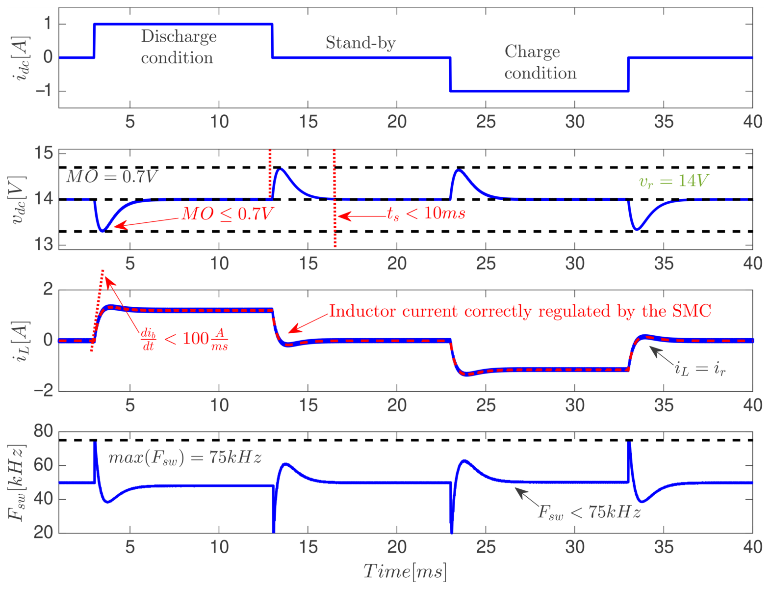
In contrast with the previous design example, this third additional design considers a much lower DC bus voltage equal to 14 V , which is used to test the system performance at low duty cycles. This application uses the same nominal battery voltage, switching frequency, maximum current derivative in the battery, and maximum settling time adopted in the previous design example Appendix A.2. Moreover, in this case, the maximum deviation of 5% corresponds to M O = 0.7 V , and the load profile is the same one used in the previous example.
Applying the design procedure reported in Section 4.4 results in an average duty cycle d = 0.16 at maximum current ( 1 A ) and a minimum inductance of 122.77 μ H , selecting the inductor value L = 330 μ H . Then, k p a = 1.11 A/V is calculated. The minimum capacitance of 253 μ F is calculated by selecting that same value of C d c = 253 μ F , which leads to a settling time t s = 3.1 ms, thus fulfilling the design requirement. Finally, k i a = 1209.6 A/(V·s) and δ S x = 0.05 A are obtained.
Figure A3 reports the simulation of this final co-design, where the correct bus regulation at 14 V , with maximum deviation M O 0.7 V and settling time t s = 3.1 ms < 10 ms observed. Moreover, the battery current derivative and switching frequency are limited as expected, i.e., d i b d t < 100 A/ms and F s w < 75 kHz. This design example considers a DC bus voltage very near to the battery voltage ( v d c is only 16.7% higher than v b ), which imposes a very small duty cycle ( d < 0.16 ). Such a small duty cycle causes peak values in the switching frequency when the bus current changes, thus requiring an additional 9% safe margin into the hysteresis band to limit the switching frequency below 75 kHz. Finally, the combination of previous (Appendix A.2) and current (Appendix A.3) examples shows the stability of the control system in a wide range of voltage conversion ratios (1.167–5.416), thus confirming the usability of the proposed co-design procedure to low-voltage and high-voltage applications.
Figure A3. Circuital simulation of the battery charger/discharger for 14 V / 1 A .
Technologies 14 00257 g0a3

Appendix B. Start-Up of the Power Stage

The first step in the start-up of a DC power system is charging the DC-bus capacitor. An unattended charge of a DC bus capacitor from the battery charger/discharger could request a large amount of current from the battery with high derivatives, even under no load at the bus. Therefore, the DC-bus capacitor is usually pre-charged to limit the inrush current. A common solution is to add a current-limiting resistor during the pre-charge phase, which is bypassed with a low-impedance switch during normal operation to avoid high conduction losses [58]. However, that technique only charges the DC-bus capacitor up to the battery voltage; thus, a second start-up phase is used to reach the desired bus voltage. The most common strategy is to control the charger/discharge at a constant duty cycle, thus limiting the battery current at a safe value [59].
Figure A4 shows a classical start-up solution for a DC-bus based on the previous two concepts. A hysteresis comparator is used to detect if the DC-bus voltage is below the minimum operation value. In the application example in Section 5, the minimum value is 12 V since the boost converter requires the bus voltage higher than the battery voltage. The bus voltage v d c is scaled down with a voltage divider as v s c a = v d c / 6 ; this enables the use of low-voltage hysteresis comparators (5 V in this case). Thus, the minimum operation voltage is also scaled down to v m i n = 2 V (representing 12 V ). When v s c a < v m i n (or v d c < 12 V ), the Reset (R) signal of the S-R Flip-Flop is activated, which forces Q = 0 . The Q output of the Flip-Flop defines the S t a r t U P signal, where S t a r t U P = 0 sets the circuit in start-up sequence, while S t a r t U P = 1 sets the circuit in normal operation.
In the start-up sequence ( S t a r t U P = 0 ), the switch S W is open, thus the resistance R c h limits the initial charging current and its derivative. Moreover, the control circuit is set to PWM mode to charge the DC-bus capacitor with limited current. Since the application example in Section 5 has an average duty cycle d = 0.52 and a maximum switching frequency F s w = 75 kHz, the same values are used to configure the start-up PWM signal.
Figure A4. Classical start-up solution for DC buses.
Technologies 14 00257 g0a4
When the DC-bus voltage reaches the nominal value v s c a = v n o m = 4 V ( v d c = 24 V in this case), the Set (S) signal of the S-R Flip-Flop is activated, forcing Q = 1 . Since S t a r t U P = 1 the circuit is set to normal operation, closing the switch S W to bypass the charging resistor R c h . Moreover, the control circuit operates in the adaptive SMC (ASMC) mode, as described in Section 3 and Section 4. It is worth noting that the control system remains in normal (ASMC) operation for the complete voltage range of the boost converter, i.e., v d c > v b = 12 V (scaled as v s c a > v m i n ).
The calculation of R c h is performed for the start-up first operation interval, where u = 0 . From the switched model (1) with u = 0 , the instantaneous DC-bus inrush current Equation (A1) is calculated, whose maximum value is given in Equation (A2), and its maximum derivative magnitude is reported in Equation (A3). Using the values defined in the example of Section 5, the minimum value R c h 4.57 Ω is needed to ensure a maximum inrush battery current of 2.5 A with a maximum derivative of 50 A/ms. In this start-up example, it is selected R c h = 5 Ω .
i b , s t a r t u p = v b R c h + R i · e t R c h + R i · C d c
max i b , s t a r t u p = v b R c h + R i
max d i b , s t a r t u p d t = v b R c h + R i 2 · C d c
The start-up time T c h is calculated from the averaged model (2) by considering the duty cycle constant and the charge resistor R c h present. Combining the inductor and capacitor equations in (2) leads to the dynamic charge model for the DC-bus capacitor given in Equation (A4). Finally, solving for the time needed to reach the nominal v d c value leads to the start-up time T c h given in Equation (A5). Using the values defined in the example of Section 5, the selected charge resistance R c h = 5 Ω and d = 0.52 , results in a start-up time T c h = 18.47 ms.
v d c , s t a r t u p = v b 1 d · 1 e t · 1 d 2 R c h + R i · C d c
T c h = R c h + R i · C d c 1 d 2 · ln 1 v d c · 1 d v b
Figure A5 shows the circuital simulation of the start-up solution designed in this appendix (Figure A4) for the example of Section 5. The simulation starts with the DC-bus capacitor discharged ( v d c = 0 V ), which sets the system in start-up condition ( S t a r t U P = 1 ). Therefore, the inrush current grows fast to reach the maximum current ( 2.2 A in this case) with a maximum derivative of 30.9 A/ms, thus fulfilling the restriction of the maximum current derivative (<50 A/ms). Moreover, S t a r t U P = 1 disables the ASMC module and activates the PWM module with d = 0.52 and F s w = 75 kHz. Since the DC-bus voltage grows following the first-order system of Equation (A4), then the battery current ( i b = i L ) also decreases as a first-order system, thus imposing a limited start-up current. Finally, the simulation confirms that the start-up occurs with a PWM operating at F s w = 75 kHz.
Figure A5. Start-up of the 24 V DC bus.
Technologies 14 00257 g0a5
When the DC bus voltage reaches the nominal value ( 24 V in this case), the hysteresis comparator sets S t a r t U P = 1 , thus terminating the start-up sequence. This activates the ASMC for normal operation (also disabling the PWM mode). The simulation confirms the accuracy of Equation (A5) for the calculation of T c h = 18.47 ms. Moreover, the simulation also shows that S t a r t U P = 1 activates the ASMC because the switching function S x starts sliding within the hysteresis band, which reduces the switching frequency. Finally, after T c h = 18.47 ms, the DC-bus capacitor is charged at nominal voltage, the ASMC is operational, and the sources and loads can be connected to the DC-bus.

References

  1. Kalair, A.; Abas, N.; Saleem, M.; Kalair, A.; Khan, N. Role of energy storage systems in energy transition from fossil fuels to renewables. Energy Storage 2020, 3, e135. [Google Scholar] [CrossRef] [Scilit]
  2. Maia, L.K.; Zondervan, E. Optimization of energy storage and system flexibility in the context of the energy transition: Germany’s power grid as a case study. BMC Energy 2019, 1, 9. [Google Scholar] [CrossRef] [Scilit]
  3. McPherson, M.; Johnson, N.; Strubegger, M. The role of electricity storage and hydrogen technologies in enabling global low-carbon energy transitions. Appl. Energy 2018, 216, 649–661. [Google Scholar] [CrossRef] [Scilit]
  4. Kittner, N.; Lill, F.; Kammen, D. Energy storage deployment and innovation for the clean energy transition. Nat. Energy 2017, 2, 17125. [Google Scholar] [CrossRef] [Scilit]
  5. Schuster, S.; Bach, T.; Fleder, E.; Müller, J.; Brand, M.; Sextl, G.; Jossen, A. Nonlinear aging characteristics of lithium-ion cells under different operational conditions. J. Energy Storage 2015, 1, 44–53. [Google Scholar] [CrossRef] [Scilit]
  6. Ibrahim, A.; Xu, J.; Al-Shamma’a, A.; Farh, H.; Aboudrar, I.; Oubail, Y.; Alaql, F.; Alfraidi, W. Optimized Energy Management Strategy for an Autonomous DC Microgrid Integrating PV/Wind/Battery/Diesel-Based Hybrid PSO-GA-LADRC Through SAPF. Technologies 2024, 12, 226. [Google Scholar] [CrossRef] [Scilit]
  7. Gabbar, H.; Othman, A.; Abdussami, M. Review of Battery Management Systems (BMS) Development and Industrial Standards. Technologies 2021, 9, 28. [Google Scholar] [CrossRef] [Scilit]
  8. Ma, T.; Sun, Z.; Han, C.; Wang, Y.; Zhang, B.; Zhang, J.; Chen, L.; Dai, X.; Zhang, S.; Shen, S. Study on the evolution of internal resistance and entropy-thermal coefficients during the aging process of lithium-ion traction batteries. e-Prime-Adv. Electr. Eng. Electron. Energy 2025, 12, 100962. [Google Scholar] [CrossRef] [Scilit]
  9. Madani, S.; Shabeer, Y.; Allard, F.; Fowler, M.; Ziebert, C.; Wang, Z.; Panchal, S.; Chaoui, H.; Mekhilef, S.; Dou, S.; et al. A Comprehensive Review on Lithium-Ion Battery Lifetime Prediction and Aging Mechanism Analysis. Batteries 2025, 11, 127. [Google Scholar] [CrossRef] [Scilit]
  10. Wang, T.; Wang, H.; Shen, X.; Lu, C.; Pei, L.; Xu, Y.; Wang, W.; Li, H. Review of Aging Mechanism and Diagnostic Methods for Lithium-Ion Batteries. Energies 2025, 18, 3884. [Google Scholar] [CrossRef] [Scilit]
  11. Raj, P.; Richter, E.; Herb, F.; Kempf, J.; Michel, F.; Birke, K. Electrochemical and aging model of li-ion batteries and estimation of total number of cycles during the lifecycle of the battery. e-Prime-Electr. Eng. Electron. Energy 2024, 9, 100712. [Google Scholar] [CrossRef] [Scilit]
  12. Li, Y.; Guo, W.; Stroe, D.; Zhao, H.; Kjær Kristensen, P.; Rosgaard Jensen, L.; Pedersen, K.; Gurevich, L. Evolution of aging mechanisms and performance degradation of lithium-ion battery from moderate to severe capacity loss scenarios. Chem. Eng. J. 2024, 498, 155588. [Google Scholar] [CrossRef] [Scilit]
  13. Santos, D.; Rezaei, S.; Zhang, D.; Luo, Y.; Lin, B.; Balakrishna, A.; Xu, B.; Banerjee, S. Chemistry–mechanics–geometry coupling in positive electrode materials: A scale-bridging perspective for mitigating degradation in lithium-ion batteries through materials design. Chem. Sci. 2023, 14, 458–484. [Google Scholar] [CrossRef] [Scilit]
  14. Pender, J.; Jha, G.; Youn, D.; Ziegler, J.; Andoni, I.; Choi, E.; Heller, A.; Dunn, B.; Weiss, P.; Penner, R.; et al. Electrode Degradation in Lithium-Ion Batteries. ACS Nano 2020, 14, 1243–1295. [Google Scholar] [CrossRef] [Scilit]
  15. Vetter, J.; Novák, P.; Wagner, M.; Veit, C.; Möller, K.; Besenhard, J.; Winter, M.; Wohlfahrt-Mehrens, M.; Vogler, C.; Hammouche, A. Ageing mechanisms in lithium-ion batteries. J. Power Sources 2005, 147, 269–281. [Google Scholar] [CrossRef] [Scilit]
  16. Baicu, L.; Andrei, M.; Dumitrascu, B. Microcontroller-Based Platform for Lithium-Ion Battery Charging and Experimental Evaluation of Charging Strategies. Technologies 2025, 13, 178. [Google Scholar] [CrossRef] [Scilit]
  17. Jeong, I.; An, S.; Kang, C. Thermal runaway behaviors in 18,650 LiFePO4 batteries under high C-rate charge/discharge operations. Appl. Therm. Eng. 2026, 289, 129760. [Google Scholar] [CrossRef] [Scilit]
  18. Ouyang, D.; Huang, J.; Zheng, Y.; Wang, Z. Numerical simulation and analysis of the effect of charging and discharging on the thermal runaway of lithium-ion batteries under external heating conditions. Appl. Therm. Eng. 2025, 274, 126616. [Google Scholar] [CrossRef] [Scilit]
  19. Huang, Y.; Xu, W.; Shen, X.; Zhao, Y.; Cao, Y.; Bai, W.; Wang, J.; Lu, Y.; Wang, Z. Investigating the impact of different abuse methods on the thermal runaway behavior of lithium batteries under high-rate charge and discharge conditions. Process Saf. Environ. Prot. 2026, 211, 108787. [Google Scholar] [CrossRef] [Scilit]
  20. Ramos-Paja, C.; Serna-Garcés, S.; Saavedra-Montes, A. Battery Power Interface to Mitigate Load Transients and Reduce Current Harmonics for Increasing Sustainability in DC Microgrids. Sustainability 2025, 17, 7987. [Google Scholar] [CrossRef] [Scilit]
  21. Papageorgiou, P.; Oureilidis, K.; Tsakiri, A.; Christoforidis, G. A Modified Decentralized Droop Control Method to Eliminate Battery Short-Term Operation in a Hybrid Supercapacitor/Battery Energy Storage System. Energies 2023, 16, 2858. [Google Scholar] [CrossRef] [Scilit]
  22. Huang, Y.; Zhao, Y.; Xu, W.; Bai, W.; Shen, X.; Wang, J.; Lu, Y.; Wang, Z. Study on the influence of high-rate charge/discharge cycle numbers and spacing on thermal runaway propagation in lithium-ion batteries. J. Energy Storage 2025, 115, 116005. [Google Scholar] [CrossRef] [Scilit]
  23. Das, P. A Perspective on the Challenges and Prospects of Realizing the Second Life of Retired EV Batteries. Batteries 2025, 11, 176. [Google Scholar] [CrossRef] [Scilit]
  24. Gu, X.; Bai, H.; Cui, X.; Zhu, J.; Zhuang, W.; Li, Z.; Hu, X.; Song, Z. Challenges and opportunities for second-life batteries: Key technologies and economy. Renew. Sustain. Energy Rev. 2024, 192, 114191. [Google Scholar] [CrossRef] [Scilit]
  25. Buidin, T.; Cristea, M.; Cristea, C. Prediction of Retired EV Batteries’ Usable Capacity for Repurposing in Second-Life Applications. Technologies 2026, 14, 124. [Google Scholar] [CrossRef] [Scilit]
  26. Alam, M.; Kumar, K. Power Management Scheme Based on Aging Factor of Battery Storage Systems for Electric Vehicles. e-Prime-Adv. Electr. Eng. Electron. Energy 2024, 9, 100710. [Google Scholar] [CrossRef] [Scilit]
  27. Gómez-González, M.; Tostado-Véliz, M.; Valverde, M.; Jurado, F. Optimal Design of Photovoltaic Domestic Installations Considering Second-Purpose Batteries. IEEE Access 2023, 11, 140126–140137. [Google Scholar] [CrossRef] [Scilit]
  28. Sethuraman, R.; Rudhramoorthy, M. Performance of bidirectional ON-Board Charger in Electric Vehicle: A review. e-Prime-Adv. Electr. Eng. Electron. Energy 2024, 8, 100613. [Google Scholar] [CrossRef] [Scilit]
  29. Park, S.; Kwak, B.; Kim, J.; Kim, I.-D. Controller Design of Multi-Modular DAB Converter for Battery Charger and Discharger. In Proceedings of the 2023 26th International Conference on Electrical Machines and Systems (ICEMS), Zhuhai, China, 5–8 November 2023; IEEE: New York, NY, USA, 2023; pp. 4644–4648. [Google Scholar]
  30. Park, S.; Kim, I.-D.; Song, S.-M.; Kim, J. Design of Battery Charger and Discharger using Series-input and Parallel-output connected DAB Converter. In Proceedings of the 2022 25th International Conference on Electrical Machines and Systems (ICEMS), Chiang Mai, Thailand, 29 November–2 December 2022; IEEE: New York, NY, USA, 2022; pp. 1–5. [Google Scholar]
  31. Ali, A.; Chuanwen, J.; Yan, Z.; Habib, S.; Khan, M.M. An efficient soft-switched vienna rectifier topology for EV battery chargers. Energy Rep. 2021, 7, 5059–5073. [Google Scholar] [CrossRef] [Scilit]
  32. Bayati, M.; Abedi, M.; Farahmandrad, M.; Gharehpetian, G.B.; Tehrani, K. Important Technical Considerations in Design of Battery Chargers of Electric Vehicles. Energies 2021, 14, 5878. [Google Scholar] [CrossRef] [Scilit]
  33. Gorji, S.; Sahebi, H.G.; Ektesabi, M.; Rad, A.B. Topologies and Control Schemes of Bidirectional DC–DC Power Converters: An Overview. IEEE Access 2019, 7, 117997–118019. [Google Scholar] [CrossRef] [Scilit]
  34. Mounika, K.; Bhattacharjee, A. Design and experimental validation for performance analysis of non-isolated power converter topologies in fuel cell integrated dynamic load based local energy systems. Energy 2025, 322, 135576. [Google Scholar] [CrossRef] [Scilit]
  35. Nava-Bustamante, M.; Meza-Medina, J.; Loera-Palomo, R.; Hernández-Jacobo, C.; Morales-Saldaña, J. A Robust Lyapunov-Based Control Strategy for DC–DC Boost Converters. Algorithms 2025, 18, 705. [Google Scholar] [CrossRef] [Scilit]
  36. K, K.; V, L.D.; Avagaddi, P.; K, K.M. Design and evaluation of power converter for integration of lithium-ion battery and renewable sources. Results Eng. 2025, 25, 104409. [Google Scholar] [CrossRef] [Scilit]
  37. Serna-Garcés, S.I.; Gonzalez Montoya, D.; Ramos-Paja, C.A. Control of a Charger/Discharger DC/DC Converter with Improved Disturbance Rejection for Bus Regulation. Energies 2018, 11, 594. [Google Scholar] [CrossRef] [Scilit]
  38. Ramos-Paja, C.; Bastidas-Rodríguez, J.D.; González, D.; Acevedo, S.; Peláez-Restrepo, J. Design and Control of a Buck–Boost Charger-Discharger for DC-Bus Regulation in Microgrids. Energies 2017, 10, 1847. [Google Scholar] [CrossRef] [Scilit]
  39. Zhang, G.; Yu, S.S.; Chen, W.; Zhang, B.; Zhang, Y. A General Polynomial Reverse Design of Step-Up Converters for EV Battery Applications. IEEE Trans. Veh. Technol. 2022, 71, 2628–2638. [Google Scholar] [CrossRef] [Scilit]
  40. Ahmadi, F.; Bizzarri, F.; Batmani, Y.; Brambilla, A.; Bevrani, H. Observer-based adaptive controller design for DC/DC buck converter interfaced DC microgrids feeding constant power loads. Electr. Power Syst. Res. 2026, 254, 112629. [Google Scholar] [CrossRef] [Scilit]
  41. Hernández, F.; Chiang, L.; Corbalán, P. A general architecture for electric power management of small scale NCRE converters: Design methodology and validation. Energy Sustain. Dev. 2017, 41, 128–138. [Google Scholar] [CrossRef] [Scilit]
  42. Makar, M.; Abdellatif, S. Low-power DC-DC converters for smart and environmentally-friendly electric vehicles: Design, simulation, and fabrication on a glass substrate. e-Prime-Electr. Eng. Electron. Energy 2024, 8, 100629. [Google Scholar] [CrossRef] [Scilit]
  43. Hinov, N.; Grigorova, T. Design Considerations of Multi-Phase Buck DC-DC Converter. Appl. Sci. 2023, 13, 11064. [Google Scholar] [CrossRef] [Scilit]
  44. Ramos-Paja, C.A.; Bastidas-Rodriguez, J.D.; Saavedra-Montes, A.J. Design and Control of a Battery Charger/Discharger Based on the Flyback Topology. Appl. Sci. 2021, 11, 10506. [Google Scholar] [CrossRef] [Scilit]
  45. Haidar, A.; Macaulay, J.; Zhou, Z. Grid-Connected Bidirectional Off-Board Electric Vehicle Fast-Charging System. Energies 2025, 18, 5913. [Google Scholar] [CrossRef] [Scilit]
  46. Guo, N.; Liu, J.; Du, S.; Li, C.; Chen, H.; Deng, Z. Design Methodology of Three-Phase LLC Charg. Based Time-Domain Model Enhanc. Anal. Accuracy Power Efficiency. IEEE Trans. Power Electron. 2025, 40, 7042–7057. [Google Scholar] [CrossRef] [Scilit]
  47. Jo, C.; Li, G.; Kim, D. Design Methodology for Bidirectional CLLC Resonant Converter with Dual Resonant Frequencies for Wide Voltage Range. IEEE Trans. Power Electron. 2024, 39, 2372–2384. [Google Scholar] [CrossRef] [Scilit]
  48. Mirtchev, A.; Tatakis, E. Design Methodology Based on Dual Control of a Resonant Dual Active Bridge Converter for Electric Vehicle Battery Charging. IEEE Trans. Veh. Technol. 2022, 71, 2691–2705. [Google Scholar] [CrossRef] [Scilit]
  49. Sha, D.; Xu, G.; Xu, Y. Utility Direct Interfaced Charger/Discharger Employing Unified Voltage Balance Control for Cascaded H-Bridge Units and Decentralized Control for CF-DAB Modules. IEEE Trans. Ind. Electron. 2017, 64, 7831–7841. [Google Scholar] [CrossRef] [Scilit]
  50. Sha, D.; Lin, Q.; You, F.; Wang, X.; Xu, G. A ZVS Bidirectional Three-Level DC–DC Converter with Direct Current Slew Rate Control of Leakage Inductance Current. IEEE Trans. Ind. Appl. 2016, 52, 2368–2377. [Google Scholar] [CrossRef] [Scilit]
  51. Montenegro-Oviedo, J.; Ramos-Paja, C.A.; Orozco-Gutierrez, M.L.; Franco-Mejía, E.; Serna-Garcés, S.I. Experimental Design of an Adaptive LQG Controller for Battery Charger/Dischargers Featuring Low Computational Requirements. World Electr. Veh. J. 2023, 14, 142. [Google Scholar] [CrossRef] [Scilit]
  52. Henao-Bravo, E.; Ramos-Paja, C.; Serna-Garcés, S. Co-Design of the Power Stage and Adaptive Controller of a Charger/Discharger to Ensure Stability and Battery Safety. In Proceedings of the 2025 IEEE 16th Latin America Symposium on Circuits and Systems (LASCAS), Bento Gonçalves, Brazil, 25–28 February 2025; IEEE: New York, NY, USA, 2025; pp. 1–4. [Google Scholar] [CrossRef] [Scilit]
  53. Villanueva-Loredo, J.; Rosas-Caro, J.; Martinez-Rodriguez, P.; Rodriguez-Cortes, C.; Langarica-Cordoba, D.; Vazquez-Guzman, G. Improved Operation of the Modified Non-Inverting Step-Down/Up (MNI-SDU) DC-DC Converter. Micromachines 2025, 16, 1063. [Google Scholar] [CrossRef] [Scilit]
  54. Ahmed, A.; Lee, Y.; Al Dawsari, S.; Diab, A.; Ezzat, A. Energy Management and Power Distribution for Battery/Ultracapacitor Hybrid Energy Storage System in Electric Vehicles with Regenerative Braking Control. Math. Comput. Appl. 2025, 30, 82. [Google Scholar] [CrossRef] [Scilit]
  55. Huerta-Moro, S.; Tavizón-Aldama, J.; Tlelo-Cuautle, E. FPGA Implementation of Sliding Mode Control and Proportional-Integral-Derivative Controllers for a DC–DC Buck Converter. Technologies 2024, 12, 184. [Google Scholar] [CrossRef] [Scilit]
  56. Sira-Ramirez, H. Sliding motions in bilinear switched networks. IEEE Trans. Circuits Syst. 1987, 34, 919–933. [Google Scholar] [CrossRef] [Scilit]
  57. IEC 60364-7-710:2021; Low-Voltage Electrical Installations—Part 7-710: Requirements for Special Installations or Locations—Medical Locations. International Electrotechnical Commission: Geneva, Switzerland, 2021.
  58. Gao, D.; Fu, F. DC-Link Capacitor Pre-Charge Designs in Automotive Systems; Texas Instruments—Application Note. SDAA145; Texas Instruments: Dallas, TX, USA, 2025; pp. 1–16. Available online: https://www.ti.com/lit/an/sdaa145/sdaa145.pdf?ts=1775193038594 (accessed on 13 April 2026).
  59. Johns, B. TPS61020 Boost Converter Start-Up and Precharge; Texas Instruments—Application Note. SLVA387; Texas Instruments: Dallas, TX, USA, 2010; pp. 1–5. Available online: https://www.ti.com/lit/an/slva387/slva387.pdf?ts=1775223085327 (accessed on 13 April 2026).
  60. Azpurua, M.; Pous, M.; Silva, F. Time- and Frequency-Domain Characterization of Switching Losses in GaN FETs Power Converters. IEEE Trans. Power Electron. 2022, 37, 3219–3232. [Google Scholar] [CrossRef] [Scilit]
  61. GeneSiC Semiconductor Inc. GeneSiC Semiconductor G3R75MT12D 1200 V 75 MiliOhm SiC MOSFET—Silicon Carbine MOSFET N-Channel Enhancement Mode; GeneSiC Semiconductor, Inc.: Dulles, VA, USA, 2023; Available online: https://genesicsemi.com/sic-mosfet/G3R75MT12D/G3R75MT12D.pdf (accessed on 15 April 2026).
  62. Shen, Y.; Qin, Z.; Wang, H. Chapter 3—Modeling and Control of DC-DC Converters. In Control Of Power Electronic Converters and Systems; Academic Press: Cambridge, MA, USA, 2018; pp. 69–92. [Google Scholar] [CrossRef] [Scilit]
  63. Yanarates, C.; Zhou, Z. Design and Cascade PI Controller-Based Robust Model Reference Adaptive Control of DC-DC Boost Converter. IEEE Access 2022, 10, 44909–44922. [Google Scholar] [CrossRef] [Scilit]
  64. IEEE Std 1547-2018; IEEE Standard for Interconnection and Interoperability of Distributed Energy Resources with Associated Electric Power Systems Interfaces. IEEE: Piscataway, NJ, USA, 2018; Revision of IEEE Std 1547-2003. pp. 1–138. [CrossRef] [Scilit]
  65. IEC 61000-3-12:2011+AMD1:2021 CSV; Electromagnetic Compatibility (EMC)—Part 3–12: Limits—Limits for Harmonic Currents Produced by Equipment Connected to Public Low-Voltage Systems with Input Current >16 A and <75 A per Phase. IEC: Geneva, Switzerland, 2021; IEC 61000-3-12 Consolidated Version. pp. 1–44.
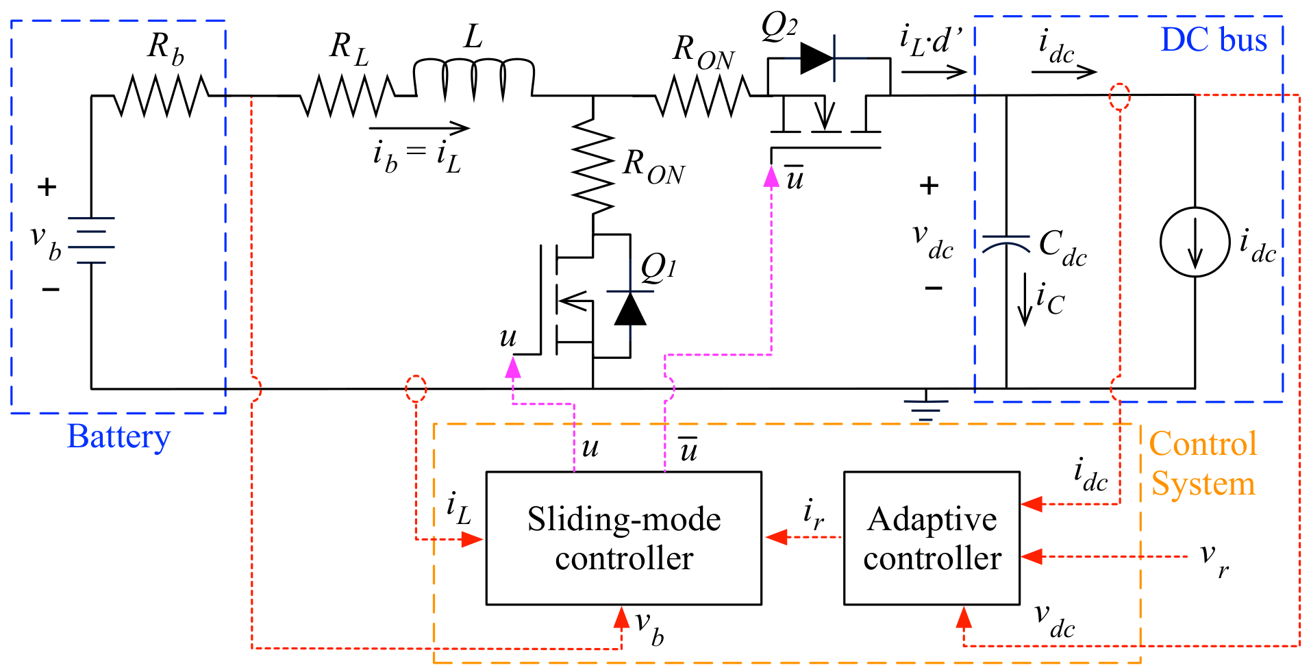
Figure 1. Charger/discharger power stage (red arrows are measured signals, magenta arrows are control signals).
Technologies 14 00257 g001
Figure 2. Equivalent closed-loop system.
Technologies 14 00257 g002
Figure 3. Co-design procedure for both the power stage and the control system.
Technologies 14 00257 g003
Figure 4. Circuital simulation of the proposed battery charger/discharger.
Technologies 14 00257 g004
Figure 5. Performance of the Adaptive SMC to parametric changes. (a) Changes in C d c . (b) Changes in L.
Technologies 14 00257 g005
Figure 6. Block diagram of the cascade PI control structure.
Technologies 14 00257 g006
Figure 7. Performance comparison between the Adaptive SMC and a Cascade PI controller. (a) Nominal v b value. (b) v b reduced by 25%.
Technologies 14 00257 g007
Figure 8. Response to a load current pulse of 500% amplitude.
Technologies 14 00257 g008
Figure 9. Physical setup of the experimental prototype.
Technologies 14 00257 g009
Figure 10. Charger/discharger operation in discharge, stand-by and charge modes.
Technologies 14 00257 g010
Figure 11. Charger/discharger operation in discharge, stand-by and charge modes with additional 220 μ F in parallel with C d c .
Technologies 14 00257 g011
Figure 12. Charger/discharger operation in discharge, stand-by and charge modes for PI control strategy.
Technologies 14 00257 g012
Figure 13. Power comparison between the Adaptive SMC and a Cascade PI controller. (a) Battery and DC bus power in discharging mode for the adaptive SMC controller. (b) Battery and DC bus power in discharging mode for PI controller. (c) Battery and DC bus power in charging mode for the adaptive SMC controller. (d) Battery and DC bus power in charging mode for PI controller.
Technologies 14 00257 g013
Figure 14. Switching frequency comparison between the Adaptive SMC and a Cascade PI controller. (a) F S W and i L ripple in the charging mode for the adaptive SMC controller. (b) F S W and i L ripple in the stand-by mode for the adaptive SMC controller. (c) F S W and i L ripple in the discharging mode for the adaptive SMC controller. (d) F S W and i L ripple in the discharging mode for PI controller.
Technologies 14 00257 g014
Figure 15. Charger/discharger operation in discharge, stand-by and charge modes with higher load power.
Technologies 14 00257 g015
Figure 16. Charger/discharger response to a load current pulse of 3 A.
Technologies 14 00257 g016
Table 1. Comparison of the contributions of this work with respect to the references reviewed. Ref., references; I. M., integrated methodology; d i / d t , battery d i / d t limitation; L. A., loss analysis; C., controller; C. T., converter topology; C. C., comparison against another controller; E. V., experimental validation.
Ref.Contributions of This Work
I. M.di/dtL. AC.C. T.C. C.E. V.
[34]×××PIBoost×
[35]×××CLF-basedBoost
[36]×××ON-OFFBoost××
[37]×××SMCBoost×
[38]××SMCBuck-Boost×
[39]×××-Boost×
[40]×××MRAC + HGOBuck×
[41]×××-Buck×
[42]×××-Buck××
[43]××-Buck××
[44]××SMCFlyback×
[45]××PIBuck-Boost××
[46]××Optimizer3 ϕ LLC
[47]×××CC − CVCLLC resonant×
[48]××PIDAB×
[49]×××PIDAB×
[50]×××DCSRZVS three-level
[51]×××LQGSEPIC/Zeta
[52]×SMC + PBoost××
Table 2. Nomenclature.
DescriptionSymbolDescriptionSymbol
Battery voltage v b DC Bus voltage v d c
Reference bus voltage v r DC Bus current i d c
Battery resistance R b MOSFET ON-resistance R O N
Converter inductanceLInductor parasitic resistance R L
DC bus capacitance C d c Input resistance R i
Inductor current i L Battery current i b
MOSFET control signaluComplementary control signal u ¯
Converter duty cycledComplementary duty cycle d
Switching frequency F s w Switching period T s w
Inductor current ripple δ i L Bus voltage ripple δ v d c
Switching function (SMC) S x Sliding surface (SMC) Q x
Reference current (SMC) i r Hysteresis width (SMC) δ S x
Adaptive proportional gain k p Adaptive integral gain k i
Normalized proportional gain k p a Normalized integral gain k i a
Bus perturbation amplitude Δ i d c Maximum overshoot M O
Settling time t s Settling time band ϵ
Conduction losses P L o s s , Ω Switching losses P L o s s , s w
MOSFET turn-ON energy E o n MOSFET turn-OFF energy E o f f
Disclaimer/Publisher’s Note: The statements, opinions and data contained in all publications are solely those of the individual author(s) and contributor(s) and not of MDPI and/or the editor(s). MDPI and/or the editor(s) disclaim responsibility for any injury to people or property resulting from any ideas, methods, instructions or products referred to in the content.