Article

Model-Based Control Assessment of PFC Systems with High-Conversion-Ratio DC–DC Converters

by
Christopher J. Rodriguez-Cortes
1,
Panfilo R. Martinez-Rodriguez
1,*,
Diego Langarica-Cordoba
2,
Gerardo Vazquez-Guzman
1,
Juan A. Villanueva-Loredo
1 and
Jose M. Sosa
3
1
Faculty of Science, Autonomous University of San Luis Potosi (UASLP), San Luis Potosi 78295, SLP, Mexico
2
Department of Electrical and Computer Engineering, The University of Texas at El Paso, El Paso, TX 79968, USA
3
Department of Electronics Engineering, ITS de Irapuato, Tecnologico Nacional de Mexico, Irapuato 36821, Gto, Mexico
*
Author to whom correspondence should be addressed.
Technologies 2026, 14(6), 314; https://doi.org/10.3390/technologies14060314

Submission received: 14 April 2026 / Revised: 20 May 2026 / Accepted: 21 May 2026 / Published: 23 May 2026
(This article belongs to the Special Issue Modeling, Design, and Control of Power Converters)

Abstract

This paper presents a model-based control strategy for a power factor correction system that employs a high conversion-ratio DC–DC converter. The proposed system consists of two stages. In the first stage, a full-bridge diode rectifier is connected to the grid through a passive filter to improve the quality of the injected current. Two passive AC input filters, namely L and L C L configurations, are evaluated to analyze their impact on grid current quality and overall system performance. The second stage is a high-step-up DC–DC converter based on the switched-inductor technique, which provides a high voltage conversion ratio. A model-based approach is employed to derive the control design from the averaged system model. The resulting control structure consists of a current tracking loop and a voltage regulation loop. A proportional-resonant controller is used to ensure current tracking and achieve a near-unity power factor, while a proportional-integral controller regulates the output voltage. Experimental validation is carried out using a low-power laboratory-scale prototype to assess the effectiveness of the proposed approach. The results demonstrate adequate current tracking and satisfactory dynamic performance within the tested operating conditions.

1. Introduction

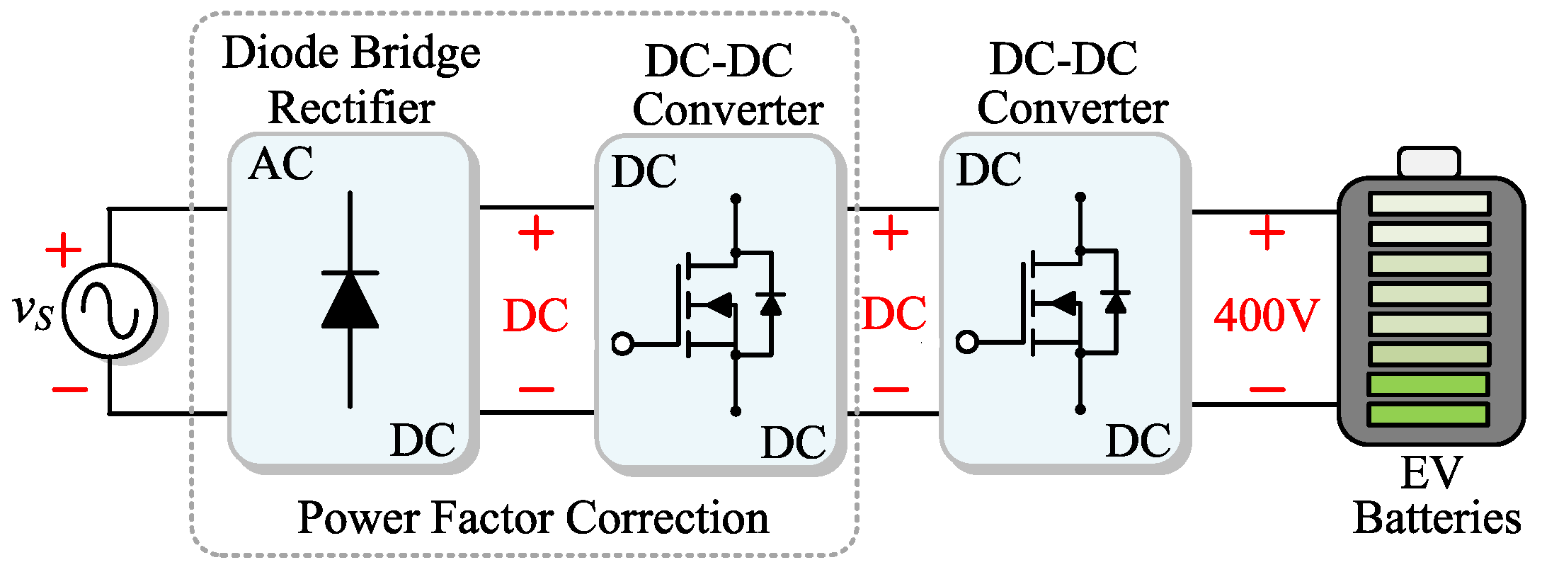
Internal combustion engine vehicles are still widely used. However, significant drawbacks are presented, including greenhouse gas emissions and dependence on fossil fuels. Therefore, the transition to cleaner alternatives has been driven by the adoption of electric vehicles (EVs) and plug-in hybrid electric vehicles (PHEVs), which have been identified as a promising solution. As a result, the growth in EV and PHEV sales has spurred the development of new technologies, particularly in battery charging systems. According to the Society of Automotive Engineers (SAE), these charging systems are classified as on-board chargers and off-board chargers [1]. On-board chargers (OBCs) are typically operated at Level 1, with power levels below 3 kW, or at Level 2, with power levels up to approximately 7–22 kW. These chargers are considered semi-fast and are supplied by single-phase or two-phase power sources. In contrast, Level 3 chargers, commonly referred to as fast chargers and generally implemented as off-board systems, are supplied by three-phase power sources and enable significantly higher power levels [2]. In particular, a structure similar to that shown in Figure 1 is commonly employed in Level 1 and Level 2 chargers.
A greater impact on the electrical grid is observed as the adoption of electric vehicles increases, leading to power quality issues, voltage instability, higher peak demand, increased losses, and transformer overload. Furthermore, harmonic distortion can be introduced into the grid current by the massive and uncoordinated connection of chargers, resulting in power factor degradation and affecting the performance of other equipment connected to the same point of common coupling. Therefore, high-performance power factor correction (PFC) is required in EV chargers to ensure a sinusoidal input current, reduce harmonic content, and improve overall system efficiency [3,4,5].
As shown in Figure 1, Level 1 and Level 2 EV chargers typically incorporate a dedicated stage to ensure power factor correction. This stage generally consists of a rectification unit followed by a DC–DC conversion stage. For this type of application, a wide variety of DC–DC converters can be employed; however, the selection of the appropriate topology depends on the specific requirements of the application, particularly the input and output voltage levels, power rating, and performance constraints. For instance, boost converters are commonly adopted in PFC applications due to their suitability for systems requiring voltage step-up capability [6,7], while Buck converters are preferred in low-voltage regulation applications [8,9]. Buck–Boost converters provide both step-up and step-down capabilities, making them suitable for systems with wide input voltage variations [10,11]. On the other hand, isolated topologies such as Flyback converters are typically employed in low- to medium-power applications requiring galvanic isolation, including battery chargers and auxiliary power supplies [12,13]. Therefore, selecting an appropriate topology is a critical design decision that directly influences the efficiency, cost, and performance of the overall system.
As previously mentioned, the conventional boost converter is widely used in PFC applications due to its simple structure, continuous input current, straightforward control scheme, and ability to achieve a high power factor [2,14]. However, despite these advantages, several drawbacks are identified, mainly related to the high electrical stress imposed on the output diode and the full-bridge rectifier. As a result, additional power losses are introduced due to the diode reverse-recovery phenomenon, which leads to a noticeable reduction in overall system efficiency [15,16]. To overcome these limitations, several PFC topologies derived from the conventional boost structure have been reported in the literature [14,16,17,18,19]. Among these alternatives, bridgeless configurations have received significant attention. In such structures, the conventional uncontrolled diode bridge is replaced by a controlled rectification stage, which reduces conduction losses and enhances the overall conversion efficiency [20,21].
For instance, in [22,23,24], several converters derived from the totem-pole topology are introduced. This configuration has been extensively adopted in PFC applications due to its high power quality, reduced component count, and compact structure, by which higher power density and improved thermal behavior are achieved [25,26]. Although the totem-pole approach has proven to be effective, with a power factor above 0.95 and an input current total harmonic distortion below 5% being ensured, certain limitations remain. Under high-power conditions, considerable stress is produced in both semiconductor devices and inductors due to elevated current levels. While this issue can be alleviated by interleaved topologies, additional complexity, cost, and a higher number of components are introduced [27,28]. Moreover, the same voltage gain as that of the conventional boost converter is provided by the totem-pole structure. Consequently, in applications such as electric vehicle chargers, where high DC bus voltages (typically around 400 V) are required, a wide step-up conversion ratio must be ensured. This condition generally results in operation at high duty cycles, by which power losses may be increased and efficiency may be negatively affected [29,30].
In this regard, the boost converter with voltage doubler has been widely adopted in PFC applications, as a higher voltage gain can be achieved without a significant increase in the duty cycle [31]. However, several disadvantages are introduced by this approach, including increased circuit complexity, the requirement for additional switching devices, higher power dissipation, and potential reliability issues, particularly under high-power conditions. In some cases, high current stresses are generated. To address the issues associated with high current stresses, multiphase converters have been proposed, by which current stresses in the semiconductor devices are reduced and system efficiency is improved, while a high voltage gain is ensured.
For instance, in [32], a two-inductor interleaved PFC boost converter is presented, in which voltage doubler operation is achieved for duty cycles greater than 0.5, making it suitable for universal input voltage ranges (90–264 Vrms). In [33], a high-gain, multilevel, interleaved, single-phase PFC boost converter based on the switched-capacitor concept is proposed. In this configuration, interphase transformers and switched-capacitor cells are incorporated to enable current sharing between branches and to significantly enhance the voltage gain. In [34], a family of hybrid SEPIC rectifiers with PFC based on switched capacitors is presented, in which semiconductor stress reduction and voltage gain enhancement are achieved through the inclusion of additional cells. Similarly, in [35], a family of three-level unidirectional PFC rectifiers based on switched capacitors is introduced, where high voltage gain and reduced semiconductor stress are obtained. However, although these topologies allow a high DC–DC conversion ratio to be ensured, together with a near-unity power factor and low total harmonic distortion, a drawback is presented due to the high number of components, by which system complexity and cost are increased.
For this reason, the switched-inductor technique has emerged as an attractive solution for achieving high conversion ratios. However, its application has been mainly limited to high-gain DC–DC converters [36,37]. Another challenge associated with boost converters in PFC applications is the injection of high-frequency harmonics into the mains current. This issue arises from the switching operation of the DC–DC stage, which introduces harmonic distortion into the input current. Therefore, an input filter is typically required to mitigate these disturbances and prevent their propagation to the power grid [38,39,40]. Moreover, conventional boost-based PFC converters rely on control strategies that simultaneously regulate the DC bus voltage and ensure power factor correction [41,42]. Although classical control methods are widely adopted, their application to high-gain converters remains limited due to increased system order and complexity. Motivated by these challenges, this work proposes a PFC system based on a high-gain DC–DC converter using the switched-inductor technique. Two passive filtering configurations, namely L-type and LCL-type, are considered to improve input current quality. In addition, a mathematical model and a model-based control strategy are developed to ensure output voltage regulation and a sinusoidal input current in phase with the grid voltage. Therefore, the leading contributions of the present work are presented as follows.
  • A model-based control strategy for a PFC system employing a high conversion ratio DC–DC converter based on the switched-inductor technique is presented.
  • An input filtering stage is incorporated between the grid and the rectifier, and a comparative evaluation between L and LCL filter configurations is carried out to assess their impact on grid current quality.
  • A control strategy derived from the averaged model is proposed, including a proportional-resonant controller for current tracking and a proportional-integral controller for output voltage regulation.
  • Experimental validation under steady-state and transient conditions is provided to demonstrate the effectiveness and performance of the proposed model-based control strategy.
The remainder of this paper is organized as follows. Section 2 introduces the description and modeling of the proposed SISUC-PFC system, including its operating principles and key analytical expressions. Section 3 presents the design methodology of the proposed control scheme, detailing both the inner current loop and the outer voltage loop. Section 4 discusses the prototype design considerations and provides experimental results to validate the performance of the proposed system under different operating conditions. Finally, Section 5 concludes the paper by summarizing the main findings and outlining directions for future work.

2. System Description and Modeling

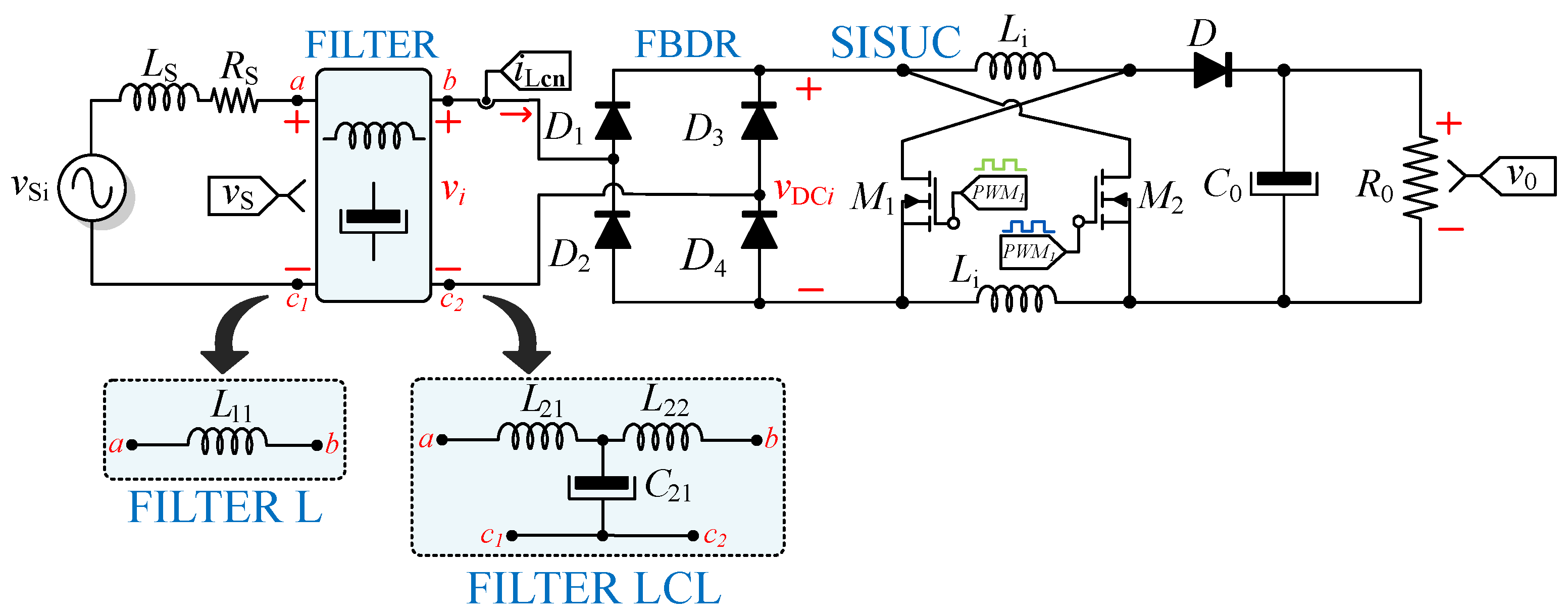
The Switched-Inductor Step-Up Converter as a PFC (SISUC-PFC) is illustrated in Figure 2. This topology is composed of two main stages, described as follows. The first stage corresponds to a full-bridge diode rectifier (FBDR) connected to the electrical grid through a passive filter. Its purpose is to improve the quality of the current injected into the grid and to supply the DC voltage required by the second stage. In this work, two passive AC input filters, an L filter and an L C L filter, interconnected to the grid, as shown in Figure 2, are evaluated to determine their impact on grid-current quality and overall system performance. The second stage is an SISUC DC–DC converter that provides a regulated output voltage v 0 . In this converter, the switched-inductor technique is employed to achieve a significantly higher voltage conversion ratio than the conventional step-up converter. The grid source is modeled through its equivalent impedance, where L S and R S represent the grid-side inductance and its associated parasitic resistance, respectively. Furthermore, v S i denotes the grid voltage, and v S denotes the voltage at the point of common coupling (PCC) with the grid.

2.1. Model of the DC–DC Stage

The system model of the SISUC-PFC converter is obtained by analyzing its two main stages separately. The first part focuses on the DC–DC conversion stage. In this analysis, the DC–DC stage is assumed to operate in continuous conduction mode (CCM), and all components are considered ideal. Additionally, all inductors in the DC–DC structure are assumed to have the same inductance values. Under these assumptions, two distinct operating modes can be identified, determined by the switching states of switches M 1 and M 2 . The first operating mode occurs when switches M 1 and M 2 are turned on, allowing the input voltage v D C i to energize the inductors L i , in which energy is stored. During this interval, diode D remains reverse-biased, and the output capacitor C 0 provides energy to the load R 0 . Conversely, in the second operating mode, switches M 1 and M 2 are turned off, thereby forward-biased diode D. In this mode, the energy previously stored in the inductors L i is released and transferred to both the output capacitor C 0 and the load R 0 . The averaged model of the DC–DC stage is derived by applying Kirchhoff’s current and voltage laws to the circuits described by the operation modes, yielding in
L i d i L i d t = u c v 0 2 + v D C i 2 ( 2 u c ) ,
C 0 d v 0 d t = u c i L i v 0 R 0 ,
where u c ( 1 d c ) represents the control signal; d c denotes the continuous PWM modulating signal (duty cycle), which takes values in the range ( 0 , 1 ) ; v D C i represents the voltage at the output of the rectification stage; i L i denotes the current flowing through the inductors L i of the DC–DC stage; and v 0 represents the output voltage. By considering (1) and (2), the steady-state conversion ratio of the DC–DC converter topology is derived as
v 0 = 1 + d 1 d v D C i .
It can be observed that the proposed converter exhibits a higher conversion ratio than the conventional DC–DC boost converter. The inductor current ripple and capacitor voltage ripple of the DC–DC stage can be calculated as follows:
Δ i L i = V D C i D L i f s w ,
Δ v C 0 = I o u t D C 0 f s w .
The critical inductor and capacitor values required to ensure continuous conduction mode (CCM) operation are given by:
L i > D R 0 ( 1 D ) 2 ( 1 + D ) f s w ,
C 0 > D 2 R 0 f s w .

2.2. Model of the Passive Filter

2.2.1. Modeling with L Filter

As shown in Figure 2, to enable the converter to operate with PFC functionality, an additional rectifier stage is incorporated. Moreover, two different types of input filters are considered for the rectifier stage. Accordingly, either an L or an L C L coupling filter is employed. To analyze the dynamic behavior of the PFC stage, the system model considering the L-filter is derived as follows:
L 11 d i L 11 d t = v S v i .
To obtain a more convenient system model structure for control scheme design, the electrical grid parameters are taken into account, and the following definition is introduced.
i L 11 i L 11 = i L 11 i L 11 = sgn ( i L 11 ) = 1 for i L 11 > 0 , undef for i L 11 = 0 , 1 for i L 11 < 0 .
Additionally, the following transformations are considered
i L i = sgn ( i L 11 ) i L 11 ,
v D C i = sgn ( i L 11 ) v S ,
e i 1 = sgn ( i L 11 ) u 1 v C 0 ,
where i L 11 represents the current flowing through the coupling inductor L 11 , and | i L 11 | denotes its absolute value. Moreover, e i 1 corresponds to the actual control input of the system. Subsequently, by applying the transformations defined in (10)–(12) to (1), the current dynamics of the SISUC-PFC equipped with an L filter are expressed in terms of the grid parameters. As a result, the current dynamics of the system shown in Figure 2 with an L filter are obtained as follows:
( L 11 + L i ) d i L 11 d t = e i 1 2 + v S δ 1 ,
where δ 1 is defined as a harmonic disturbance, given as δ 1 = u 1 v S / 2 .

2.2.2. Modeling with LCL Filter

The second case under analysis considers the system shown in Figure 2 operating with an L C L filter. This filter is composed of two inductors, L 21 and L 22 , and a capacitor C 21 . Accordingly, the input dynamics are derived by applying Kirchhoff’s current and voltage laws and are expressed as
L 21 d i L 21 d t = v C 21 + v S ,
C 21 d v C 21 d t = i L 21 i L 22 ,
L 22 d i L 22 d t = v i + v C 12 .
Furthermore, to derive a model structure more suitable for control design, and following the procedure previously applied to the current i L 11 , the following definition for i L 22 is introduced:
s g n ( i L 22 ) = 1 for i L 22 > 0 undef for i L 22 = 0 1 for i L 22 < 0 ,
and the following transformations are also considered
i L i = s g n ( i L 22 ) i L 22 ,
v D C i = s g n ( i L 22 ) v C 21 ,
e i 2 = s g n ( i L 22 ) u 2 v C 22 ,
where i L 22 represents the inductor current of L 22 and e i 2 is the control input to the system. Thus, the current dynamics of the SISUC stage, described by (1), are combined with the transformations (17) to (20), resulting in
L i d i L 22 d t = e i 2 2 + v i u 2 v C 21 2 .
Now, the current dynamics describing the inductor currents L 22 and L i 2 are obtained by considering (16) and (21), resulting in
( L i + L 22 ) d i L 22 d t = e i 2 2 + v C 21 ,
where
u 2 = e i 2 s g n ( i L 22 ) v C 22 .
Therefore, the dynamics associated with the L C L filter and the DC–DC stage current are expressed as
L 21 d i L 21 d t = v C 21 + v S ,
C 21 d v C 21 d t = i L 21 i L 22 ,
( L 22 + L i ) d i L 22 d t = e i 2 2 + v C 21 δ 2 ,
as previously mentioned, δ 2 represents a harmonic perturbation. It is important to note that the output voltage dynamics of the PFC-SISUC stage are independent of the selected input filter configuration; therefore, the output voltage dynamics of both systems are described by
C 0 d v C 0 d t = u c i L i v 0 R 0 .
To obtain a more convenient structure for control design, (2) can be reformulated in terms of the variable z i = v 0 / 2 , which represents the energy stored at the output. Hence, the output voltage dynamic can be expressed as
C 0 d z i d t = e i c i L i 2 z i R 0 .
In summary, based on the preceding analysis, the average models describing the dynamics of the SISUC-PFC system for the two considered input filter configurations are presented as follows.
For the SISUC-PFC operating with an L filter, the average model is given by
( L 11 + L i ) d i L 11 d t = e i 1 2 + v S δ 1 ,
C 12 d z 1 d t = e i 1 i L 11 2 z 1 R 0 .
Similarly, for the SISUC-PFC configuration employing an L C L filter, the corresponding average model is expressed as
L 21 d i L 21 d t = v C 21 + v S ,
C 21 d v C 21 d t = i L 21 i L 22 ,
( L 22 + L i ) d i L 22 d t = e i 2 2 + v C 21 δ 2 ,
C 22 d z 2 d t = e i 2 i L 22 2 z 2 R 0 .
Notice that, as in several PFC topologies incorporating a DC–DC converter in their structure, system controllability is not guaranteed at i c 1 = 0 . In this case, this limitation remains even after applying the proposed transformation used to obtain the representations in (29) to (34). However, this new system representation allows the control to be formulated in terms of the grid parameters, which is more convenient for practical implementation.

3. Control Design Procedure

This section presents the proposed controller design procedure for the SISUC-PFC system. The control strategy is developed to fulfill two main control objectives, namely current tracking and DC-link voltage regulation. The first objective aims to force the grid current to track a sinusoidal reference proportional to the grid voltage. To ensure accurate tracking and mitigate harmonic distortion in the grid current, a proportional-resonant controller is designed, enabling operation with a near-unity power factor. The second control objective focuses on guaranteeing proper regulation of the DC output voltage. The proposed control design strategies are described in detail in the following subsections.

3.1. Control Objectives

To design the control strategies, the following control objectives are established for the operation of the SISUC-PFC.
(i)
The Power factor compensation control objective aims to enforce the grid current to follow a desired reference proportional to the grid voltage. This control objective can be formulated as
i L cn i L cn = g c v ^ S ,
where i L cn denotes the reference current. The subindex cn is used to distinguish among the different input filters of the converter and their corresponding elements. For instance, i L 11 refers to the current flowing through inductor one of the SISUC-PFC converter with an L filter. On the other hand, g c represents the estimated apparent conductance as seen from the grid side, and is defined as
g c = p c v S , R M S 2 ,
where v S , RMS denotes the RMS value of the grid voltage. The term p c is defined as the control input generated by the voltage regulation loop, which is described in a subsequent section. The fundamental component of the grid voltage is denoted by v ^ S . To extract this component, a filtering stage is employed, whose transfer function is given by
v ^ S v S = λ G s s 2 + λ G s + ω 0 2 ,
where λ G is a constant parameter used to adjust the convergence rate of v ^ S , and ω 0 = 2 π f 0 denotes the angular frequency of the fundamental component in rad/s. It is worth noting that the fundamental component extraction mechanism also functions as a phase-locked loop (PLL), ensuring that the current reference remains in phase with the fundamental component of the grid voltage while remaining free of harmonic distortion.
(ii)
Average regulation of the DC-link voltage toward a constant reference v r e f c , i.e., v C 0 0 v r e f c . This control objective ensures the regulation of the average voltage across the capacitor C 0 to the desired constant value, where v C 0 0 denotes the average output voltage of the SISUC-PFC system. Note that this objective is equivalent to enforcing z ˜ c 0 0 .

3.2. Control Design Assumptions

Moreover, the following assumptions are taken into account to perform the controller design.
A1 
The voltage dynamics of the output capacitor v 0 are significantly slower than the remaining system dynamics, which enables the application of the time-scale separation principle. As a result, the control design can be decomposed into two independent loops: a fast inner loop dedicated to power factor correction and a slower outer loop responsible for output voltage regulation.
A2 
All PFC system parameters, namely L i , L c 1 , L c 2 , C 11 , and R 0 , are assumed to be known or to vary slowly with respect to time. In addition, possible step changes in the load are considered within the normal operating conditions of the system.
A3 
The fundamental grid frequency, denoted by f 0 , is assumed to remain constant during the converter operation.

3.2.1. Inner Loop Design for the SISUC-PFC with L Filter

This subsection presents the design procedure of the proposed control strategy for the topology shown in Figure 2, considering the use of a coupling L-filter. The current control loop is designed in accordance with the current tracking objective presented in (i). For the controller design, the system is represented in a state-space form by introducing the state variable x 11 i L 11 . Thus, the averaged model described in (29) and (30) can be rewritten as follows,
L x 1 x ˙ 11 = e i 1 2 + v S ϕ R 1 ,
C 12 z ˙ 1 = e i 1 x 11 2 z 1 R 0 ,
where L x 1 denotes the equivalent inductance, defined as L x 1 = L 11 + L i . The inner-loop control design is carried out under the decoupling assumption stated in A1; therefore, only the dynamics described in (38) are considered. The current tracking error is defined as x ˜ 11 x 11 x 11 . By direct substitution into (38), the resulting error dynamics are given by
L x 1 x ˜ ˙ 11 = e i 1 2 + v S ϕ R 1 ,
where
ϕ R 1 δ 1 + L i 1 x ˙ 11 .
It is worth noting that the term ϕ R 1 represents a harmonic disturbance composed of multiple harmonics of the fundamental frequency ω 0 . To ensure accurate current tracking in the presence of this disturbance, a controller based on (40) is proposed and defined as follows,
e i 1 = 2 ( k p i 1 x ˜ 11 + v S ϕ ^ R 1 ) .
Here, ϕ ^ R 1 is introduced as an estimate of the disturbance term ϕ R 1 , while the gain k p i 1 denotes the proportional gain of the proposed controller. This gain is selected as a positive design parameter, i.e., k p i 1 > 0 , in order to provide damping to the current dynamics. As can be observed, the controller is composed of a proportional action k p i 1 combined with the harmonic disturbance estimator ϕ ^ R 1 . In addition, a feedforward term based on the grid voltage v S is incorporated to mitigate grid-side disturbances. Consequently, the harmonic estimator ϕ ^ R 1 is implemented as a bank of resonant filters driven by the current tracking error, yielding
ϕ ^ R 1 = G ϕ , h 1 ( s ) x ˜ 11 ,
G ϕ , h 1 ( s ) = n 1 { 1 , 3 , 5 , } γ n 1 s s 2 + n 1 2 ω 2 ,
where γ n 1 is a positive design parameter.

3.2.2. Inner Loop Design for the SISUC-PFC with LCL Filter

One of the main challenges of the SISUC DC–DC converters is the presence of high input current ripple. Consequently, a first-order input filter may be insufficient, especially when the converter is connected to a weak grid. The interaction between the input current ripple and the source impedance may lead to undesirable grid-voltage effects, such as distortion. To mitigate these issues, an additional third-order filter, referred to as an L C L filter, is incorporated. This filter provides enhanced attenuation of switching-frequency ripple while enabling a reduction in the required input filter size. Thus, in this subsection, the control scheme for the topology shown in Figure 2 employing an L C L filter is presented. For the design of the current tracking loop, the system states are defined as i L 21 x 21 , v C 21 x 22 , and i L 22 x 23 . Using these definitions, the system dynamics given in (31)–(33) are rewritten in state-variable form, yielding
L 21 x ˙ 21 = x 22 + v S ,
C 21 x ˙ 22 = x 21 x 23 ,
L x 2 x ˙ 23 = e 2 i 2 + x 22 δ 2 ,
where L x 2 represents the equivalent inductance defined as L x 2 = L 22 + L i and e i 2 is the control input applied to the system. The reference trajectories of the system are represented as x 21 , x 22 , x 23 . From (45)–(47), and considering the control objectives, the references are calculated as
x 21 = g 2 v ^ S = p 2 v S , RMS v ^ S ,
x 22 = v S L 21 x ˙ 21 ,
x 23 = x 21 C 21 v ˙ s + C 21 L 21 x ¨ 21 .
Note that x 21 is defined such that the input current i L 21 follows the fundamental component of the mains voltage, ensuring a power factor close to unity. In this case, g 2 denotes the conductance at the mains side. To compute x 23 , the first derivative of the fundamental component of the input voltage v ^ ˙ S , is required. This derivative is obtained through the filter proposed in (37), which is expressed as v ^ ˙ S = ω 0 2 s v ^ s . As in the previous section, the inner-loop design is developed under the decoupling assumption stated in A1, where the output capacitor dynamics are considered slower than the remaining system dynamics. Therefore, the errors of the fast states are defined as follows
x ˜ 21 x 21 x 21 ,
x ˜ 22 x 22 x 22 ,
x ˜ 23 x 23 x 23 .
Thus, substituting (51)–(53) in (45)–(47), the model error is given as
L 21 x ˜ ˙ 21 = x ˜ 22 ,
C 21 x ˜ ˙ 22 = x ˜ 21 x ˜ 23 ,
L x 2 x ˜ ˙ 23 = e i 2 2 + x ˜ 22 + v S δ 2 ( L 21 + L x 2 ) x ˙ 21 + C 21 L x 2 ω 0 2 v S C 21 L 21 L x 2 x 21 .
Note that (56) contains terms that can be grouped as harmonic disturbances. Therefore, the system can be rewritten as
L x 2 x ˜ ˙ 23 = e i 2 2 + v S ϕ R 2 ,
where ϕ R 2 represents the grouped harmonic disturbances, expressed as
ϕ R 2 = δ 2 ( L 21 + L x 2 ) x ˙ 21 + C 21 L x 2 ω 0 2 v S C 21 L 21 L x 2 x 21 + x ˜ 22 .
To ensure reaching the current tracking objective, a control law based on the subsystem in (57) is proposed as
e i 2 = 2 ( k p , i 2 x ˜ 23 + v S ϕ ^ R 2 ) ,
here, the term ϕ R 2 captures odd harmonics of the grid frequency, and ϕ ^ R 2 is its estimation. The gain k p , i 2 is a positive proportional term that introduces damping into the system and ensures error convergence. Thus, the controller structure in (59) includes a proportional feedback term k p , i 2 x ˜ 23 , a feedforward of the grid voltage v S , and a harmonic compensator ϕ ^ R 2 to cancel grid disturbances. The harmonic compensator yields a structure of a bank of resonant filters applied to the current error, as follows:
ϕ ^ R 2 = G ϕ h 2 ( s ) x ˜ 23 ,
G ϕ h 2 ( s ) = n 2 { 1 , 3 , 5 , } γ n 2 s s 2 + n 2 2 ω 0 2 .
This structure effectively targets and attenuates odd harmonics of the grid frequency ω 0 . Furthermore, to establish the relationship between the current reference and the system states, an explicit expression for x 23 is derived from the dynamic model as follows,
x 23 = ( 1 C 21 L 21 ω 0 2 ) x 21 2 C 21 v ^ ˙ S .
This expression accounts for the effect of the output capacitor and enables the tracking of the grid current by sensing the output current of the converter x 23 . This permits the implementation of the current control loop using two signals only, the current x 23 , and the grid voltage v S . The latter contrasts with some approaches that require more than one state of the system, including v S . Nevertheless, as expected, for the voltage control loop, the output capacitor voltage v C 22 is additionally required to implement the overall control law.

3.2.3. Voltage Regulation Loop

This subsection presents the design of the voltage regulation loop for the system depicted in Figure 2, including an L C L filter. The control objective is to ensure accurate output voltage tracking. The controller is derived under assumption A1, assuming that the current error satisfies x ˜ 23 0 . Under this condition, the dynamics in (2) are reformulated in terms of the energy error defined as z ˜ 2 = Δ z 2 v r e f 2 2 / 2 . Hence, the system dynamics can be expressed as
C z ˜ ˙ 2 = 2 ( 1 C 21 L 21 ω 0 2 ) p 2 2 C 21 v ^ ˙ S v ^ S P 02 2 z ˜ 2 R C 2 .
Considering that 1 C 21 L 21 ω 0 2 , the previous expression can be approximated as
C 22 z ˜ ˙ 2 = 2 p 2 P 02 2 z ˜ 2 R c 2 .
Observed that (64) corresponds to a first-order system with p 2 as control input. The objective is to enforce z ˜ 2 0 , guaranteeing that the average output voltage converges to the reference v ref 2 . To achieve voltage regulation, a PI controller is formulated in terms of z ˜ 2 , and is defined as
p 2 = 1 2 ( k i , v 2 ξ 2 + k p , v 2 υ 2 ) ,
ξ ˙ 2 = z ˜ 2 ,
2 τ v 2 υ ˙ 2 = z ˜ 2 υ 2 ,
where ξ 2 is the integral state introduced to remove steady-state error, k i , v 2 and k p , v 2 denote the integral and proportional gains, respectively, and τ v 2 represents the time constant of the low-pass filter. This filter is implemented to attenuate the harmonic components injected into the voltage loop by the rectification stage. The transfer function of the controller is
G c , v 2 ( s ) = 1 2 k i , v 2 s + k p , v 2 τ v 2 s + 1 .
This controller enforces z ˜ 2 0 , ensuring DC voltage regulation at the reference value.

3.2.4. Overall Structure of the Proposed Control Strategies

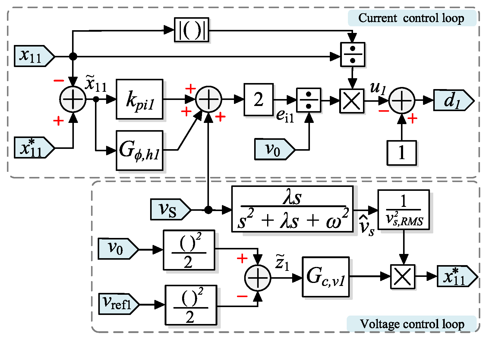
This section presents the control strategies developed for the SISUC-PFC system employing both L and L C L coupling filters to the grid. For the case of an L filter, the control architecture consists of an inner current control loop and an outer voltage control loop. The resulting control law is summarized in (69)–(74) and illustrated in Figure 3.
e i 1 = 2 ( k p , i 1 x ˜ 11 + v S ϕ ^ h 1 ) ,
ϕ ^ R 1 = G ϕ , h 1 ( s ) x ˜ 11 ,
G ϕ , h 1 ( s ) = n 1 { 1 , 3 , 5 , } γ n 1 s s 2 + n 1 2 ω 2 ,
G c , v 1 ( s ) = k i , v 1 s + k p , v 1 τ v 1 s + 1 ,
u 1 = e i 1 v C 12 i L 11 | i L 11 | ,
d 1 = 1 u 1 .
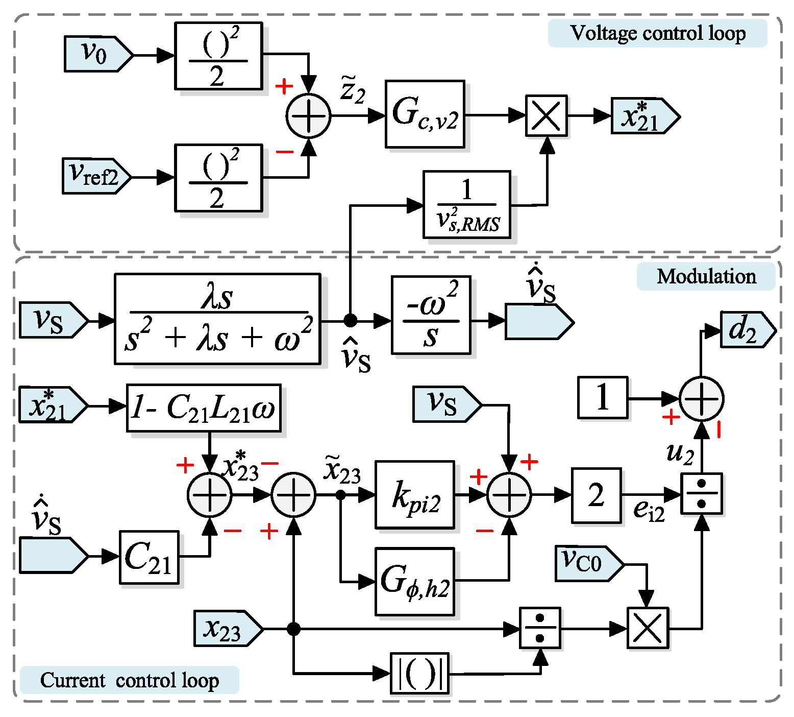
For the SISUC-PFC system employing an L C L grid filter, the overall control structure similarly incorporates current and voltage control loops. The corresponding control expressions are (75)–(80) and depicted in Figure 4.
e i 2 = 2 ( k p , i 2 x ˜ 23 + v S ϕ ^ h 2 ) ,
ϕ ^ R 2 = G ϕ , h 2 ( s ) x ˜ 23 ,
G ϕ , h 2 ( s ) = n 2 { 1 , 3 , 5 , } γ n 2 s s 2 + n 2 2 ω 2 ,
G c , v 2 ( s ) = 1 2 k i , v 2 s + k p , v 2 τ v 2 s + 1 ,
u 2 = e i 2 v C 22 i L 22 | i L 22 | ,
d 2 = 1 u 2 .

4. Experimental and Numerical Results

In this section, the numerical and experimental validation results of the proposed controllers are presented in order to verify their performance under representative operating conditions. First, the results obtained through simulations are shown, allowing the dynamic response of the system, the stability of the control loop, and the steady-state behavior under parameter variations and disturbances to be analyzed. Subsequently, the experimental results obtained from an implemented prototype are presented, through which the practical feasibility of the control strategy is corroborated.

4.1. Numerical Results

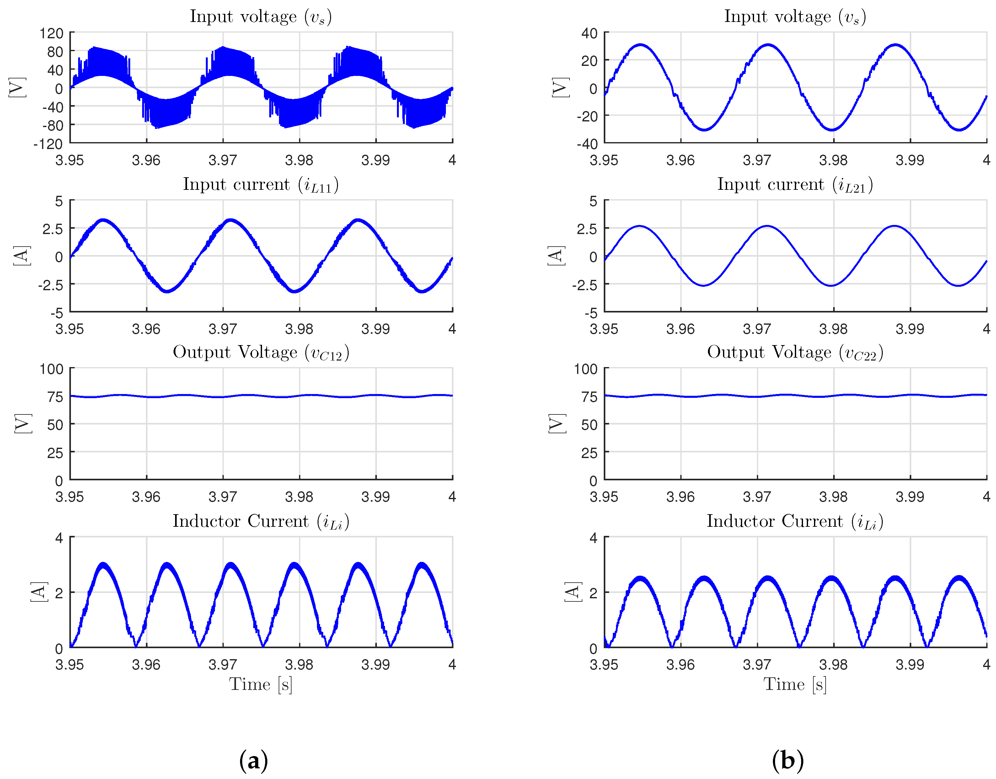
Figure 5 shows the numerical validation of the two systems together with the proposed controllers. For this validation, the parameters listed in Table 1 are considered. In Figure 5a, the steady-state response of the SISUC-PFC converter with an L filter is presented. A noticeable level of noise is observed in the input voltage. This behavior is attributed to the fact that the simulation environment is configured to replicate the conditions of the experimental setup to be implemented. In particular, the grid is replaced by a 24 V R M S transformer used as the power supply for the proposed systems. Due to the relatively high output impedance of the employed source, unlike a stiff grid, the voltage at the point of common coupling (PCC) becomes highly sensitive to switching dynamics. As a result, current ripple is directly reflected as noticeable voltage distortions, leading to the observed noise in the input voltage. However, even under these non-ideal conditions, the proposed control law demonstrates adequate performance. It can be observed that the input current i L 11 presents a sinusoidal waveform and remains in phase with the input voltage, achieving a power factor close to unity. In addition, the output voltage is regulated at the reference value of 75 V . Therefore, both control objectives are properly achieved. On the other hand, Figure 5b shows the steady-state response of the SISUC PFC system with an L C L filter. As can be observed, an improved performance is achieved compared to the L-type filter, since a lower input current ripple and a reduced THD are obtained. In addition, both control objectives, current tracking and output voltage regulation, are properly ensured. It should be noted that the L C L filter is designed considering a resonance frequency higher than the grid frequency and significantly lower than the switching frequency, thus avoiding the excitation of resonant modes under normal operating conditions.
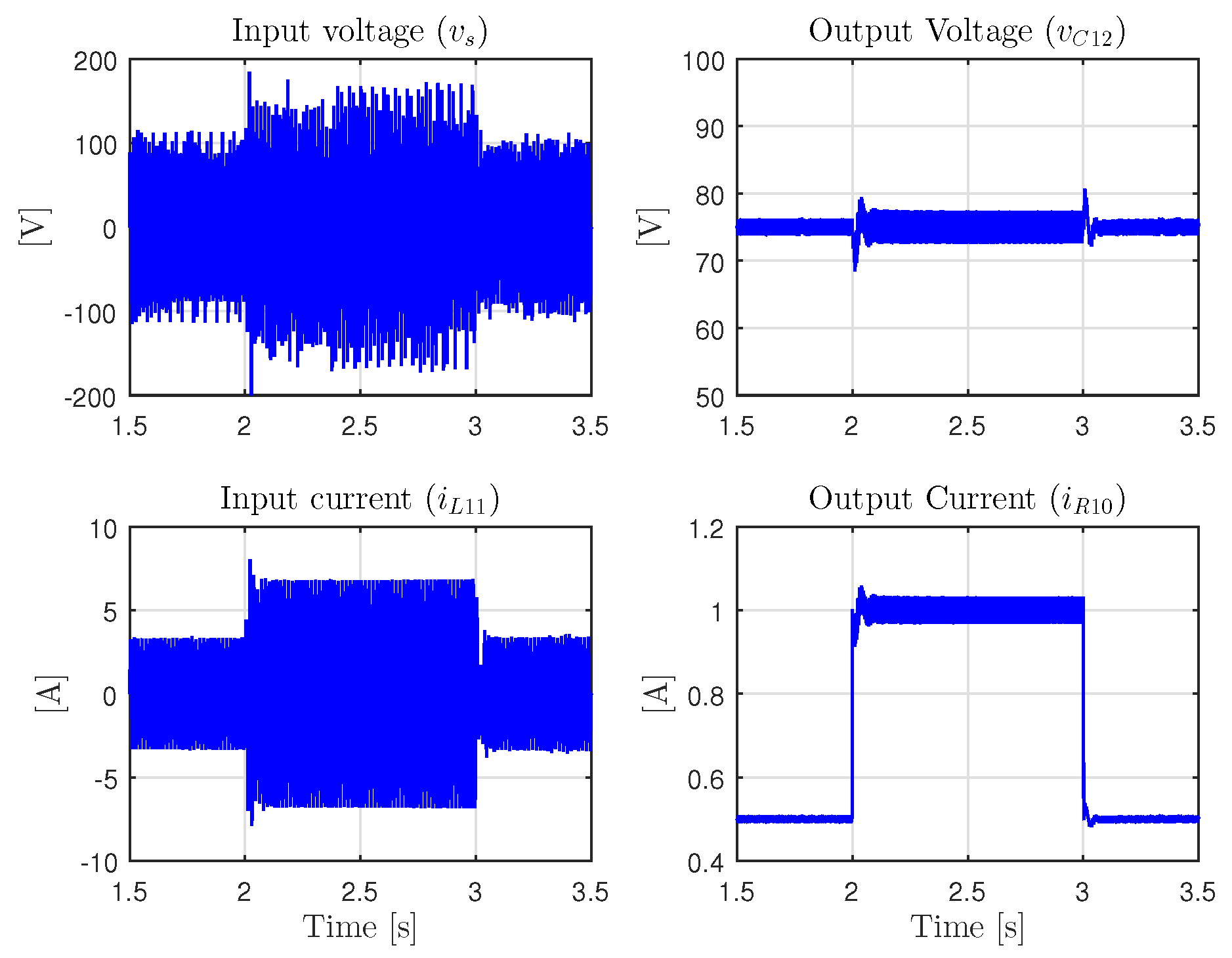
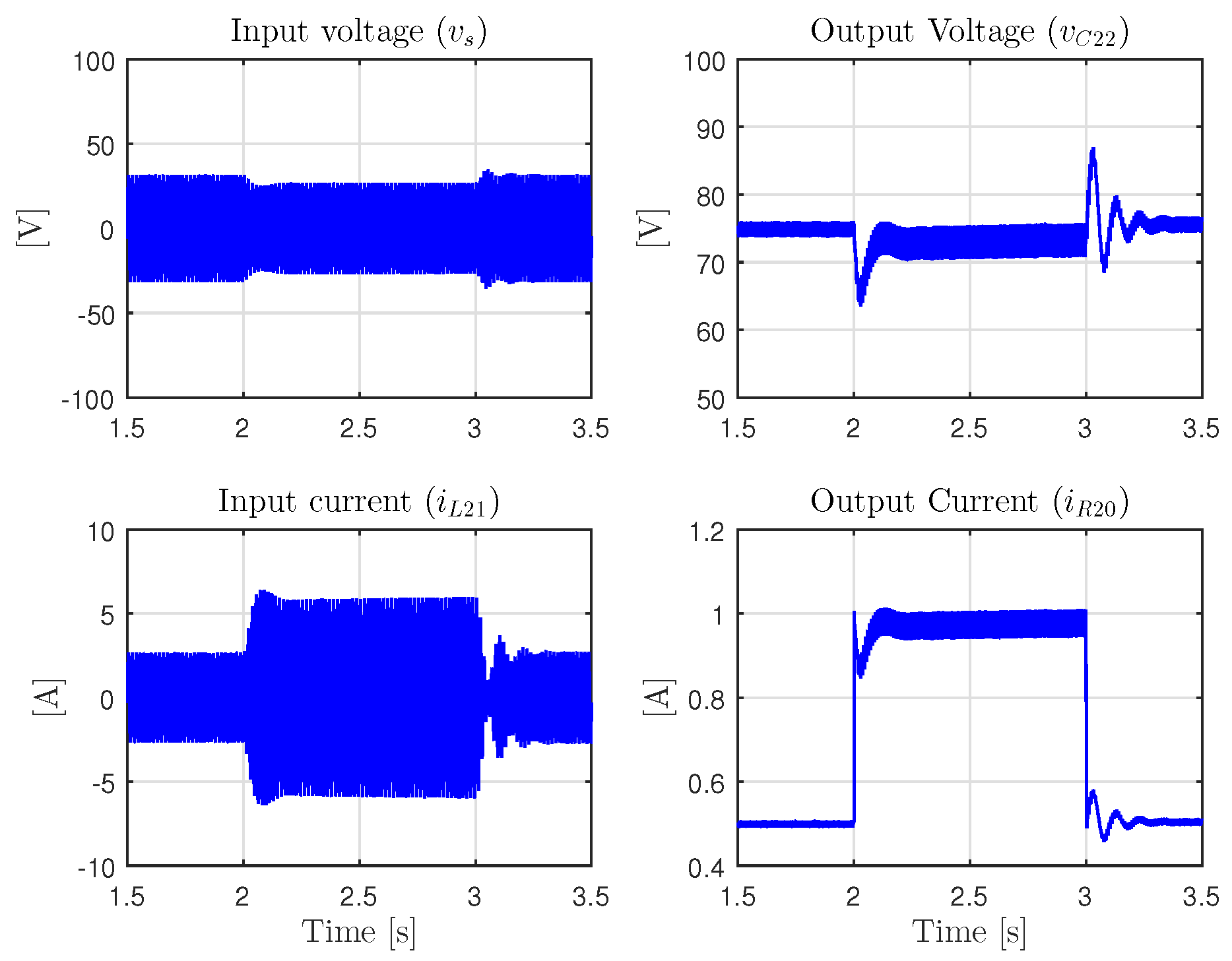
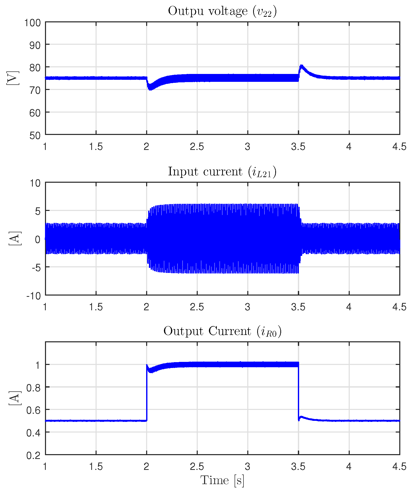
Figure 6 and Figure 7 illustrate the transient response of the proposed systems under load variations from 150 Ω to 75 Ω and from 75 Ω to 150 Ω , respectively. In both scenarios, it can be observed that the output voltage remains regulated despite the changes in load conditions, indicating that the control objectives for which the controllers were designed are effectively achieved.
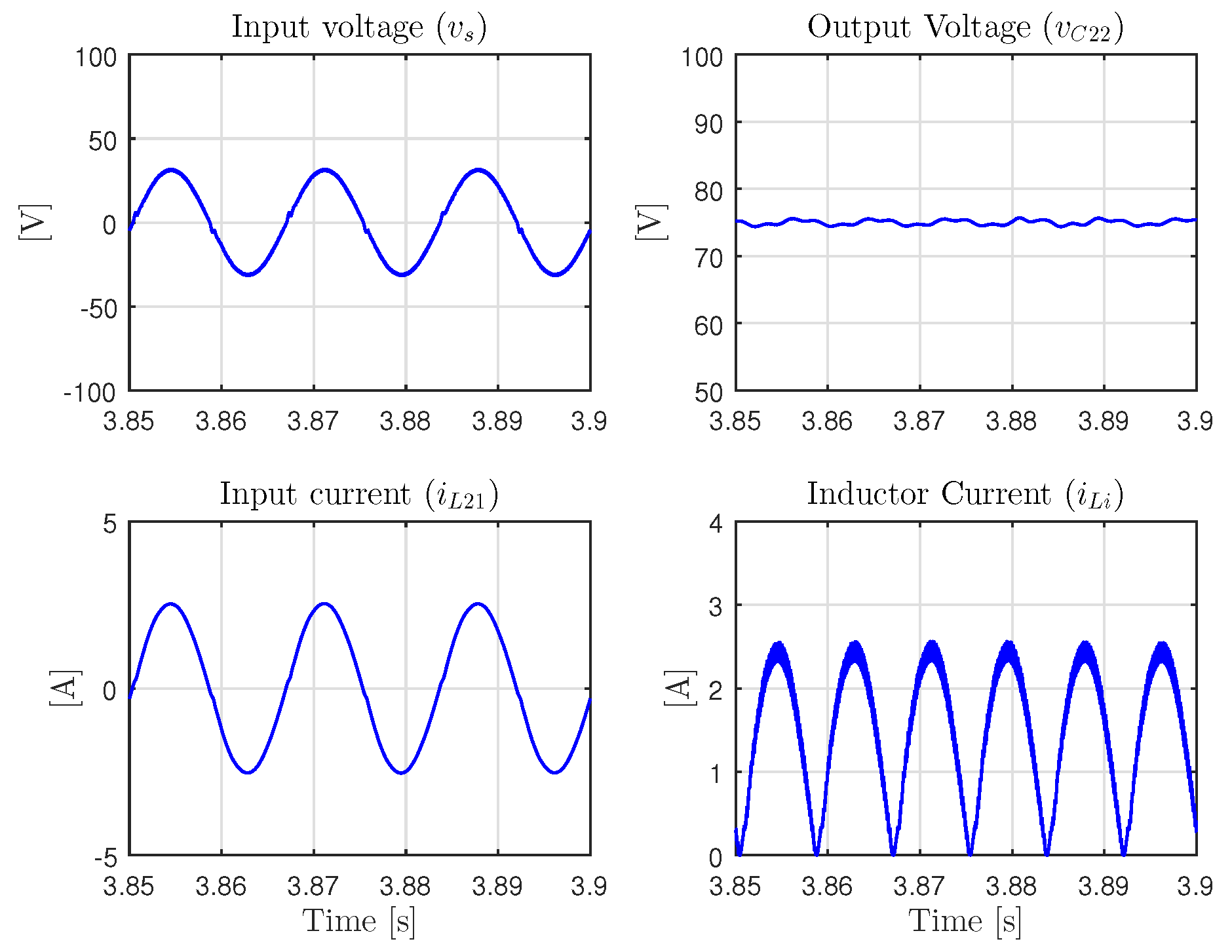
As an additional test, a nonlinear load is connected to the proposed system, particularly to the SISUC-PFC converter with an L C L filter, as shown in Figure 8. The implemented load consists of a high-frequency H-bridge followed by a 1:1 high-frequency transformer, a full-wave rectifier, and an output LC filter. The obtained results are presented in Figure 9. As can be observed, the proposed system continues to satisfy the control objectives even under nonlinear loading conditions, exhibiting an adequate performance. In particular, the input current preserves a sinusoidal waveform with low THD and a power factor close to unity, while the output voltage remains properly regulated, even under transient changes, as shown in Figure 10.

4.2. Experimental Results

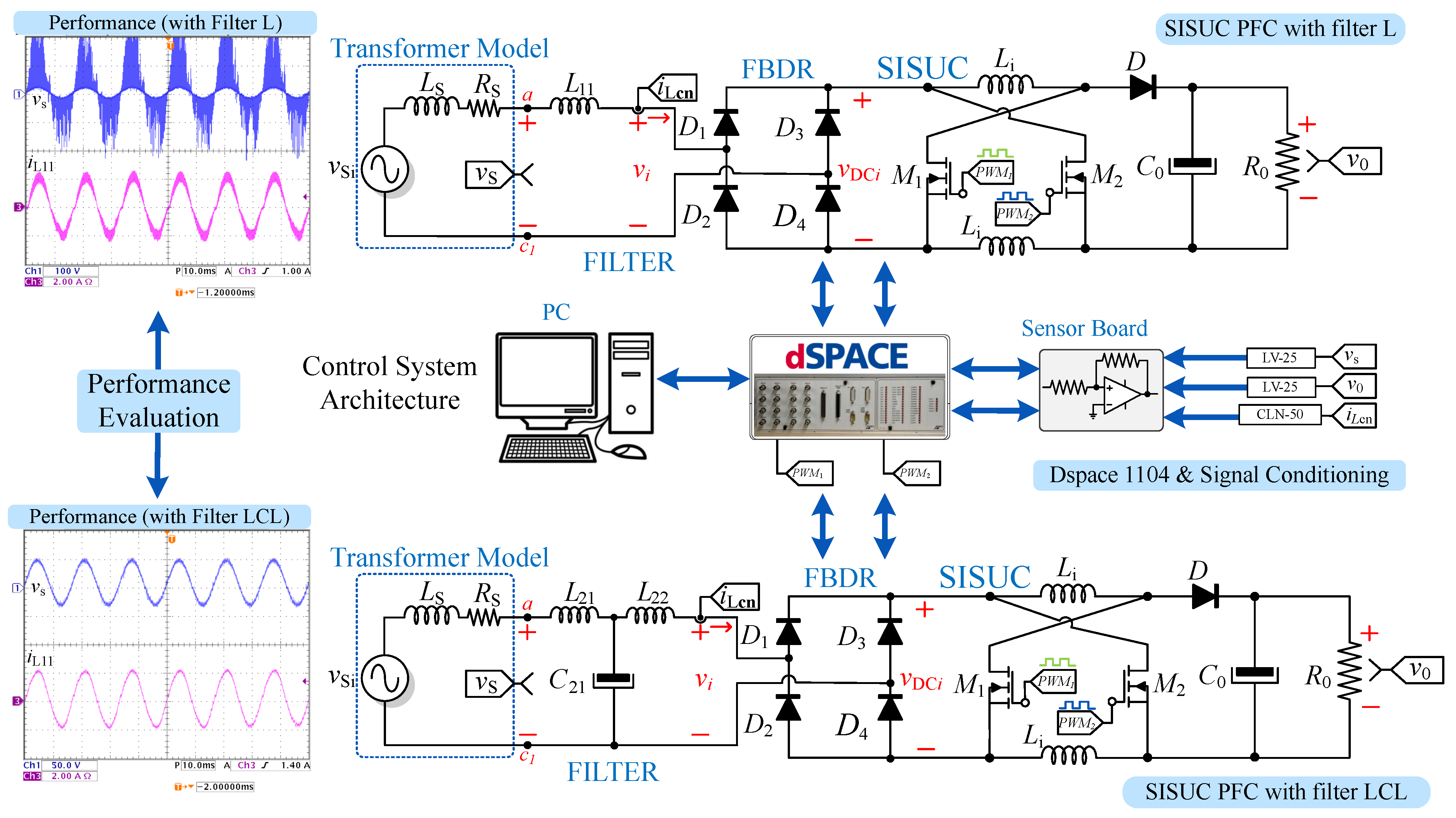
Now this subsection presents the experimental validation of the SISUC-PFC. The experimental validation is carried out using a low-power academic prototype developed as a proof of concept. The main objective of this implementation is to verify the proposed control strategy and the modeling approach of the DC–DC topology with power factor correction capability. The controller is implemented on a dSPACE 1104 DAQ board, while the switching signals are transmitted via fiber optics to guarantee electrical isolation and reduce electromagnetic interference. Current and voltage measurements are obtained through a dedicated sensing board using CLN-50 and LV-25P sensors. All signals are monitored and recorded using ControlDesk software. The block diagram of the implemented closed-loop system is shown in Figure 11. As can be observed, the system is mainly composed of the power stage and the control stage. For the experimental validation, the system parameters and the controller gain values summarized in Table 1 are considered. The performance of the converter and the controllers is evaluated under two operating scenarios: steady-state and transient conditions. It is important to highlight that the gains of both control loops are selected using a heuristic procedure based on numerical results. First, the proportional gains are set to low values and then gradually increased until the current and voltage responses approach their reference values. Subsequently, the integral gains are progressively increased to eliminate the steady-state error.
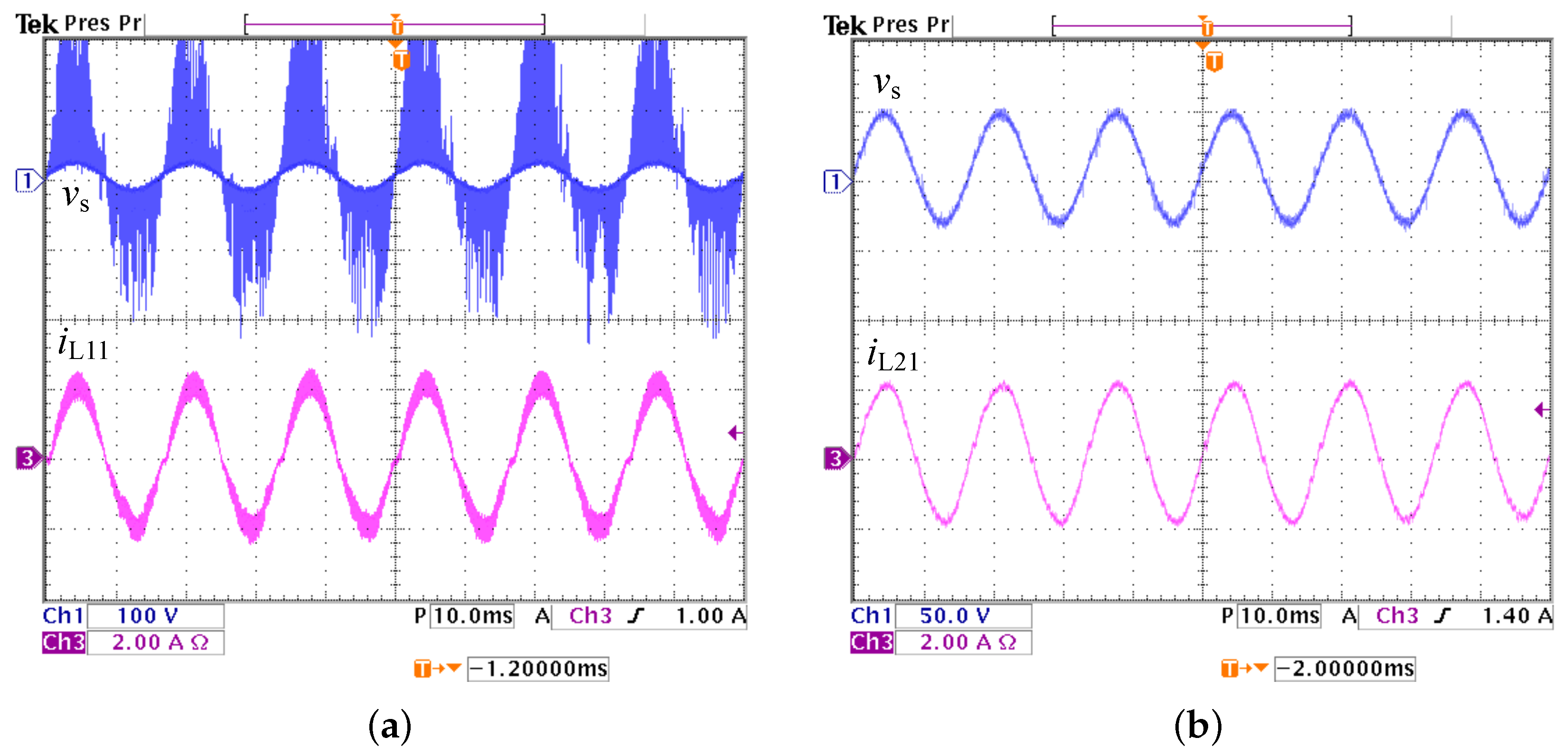
Figure 12 shows the steady-state grid voltage and line current of the SISUC-PFC using L and L C L input filters. Figure 12a corresponds to the L-filter case. The line current is sinusoidal and in phase with the grid voltage, resulting in a power factor close to 0.9. Some distortion in the grid voltage v S is observed, which is attributed to the transformer impedance. However, this distortion is not reflected in the line current, since no distortion is observed in its waveform. Furthermore, Figure 12b shows the steady-state response of the grid voltage and line current of the SISUC-PFC converter with an L C L filter. As observed, the grid voltage and current are in phase, yielding a power factor of 0.99. In particular, the use of the L C L filter provides improved performance in terms of grid current THD, current ripple levels Δ i 21 , and power factor compared to the L-filter case. As shown in Figure 12b, the grid current i L 21 exhibits a reduced switching ripple, which lowers the harmonic content and directly contributes to the improvement of the THD. Consequently, the L C L filter enhances the grid current quality and the overall performance of the PFC converter.
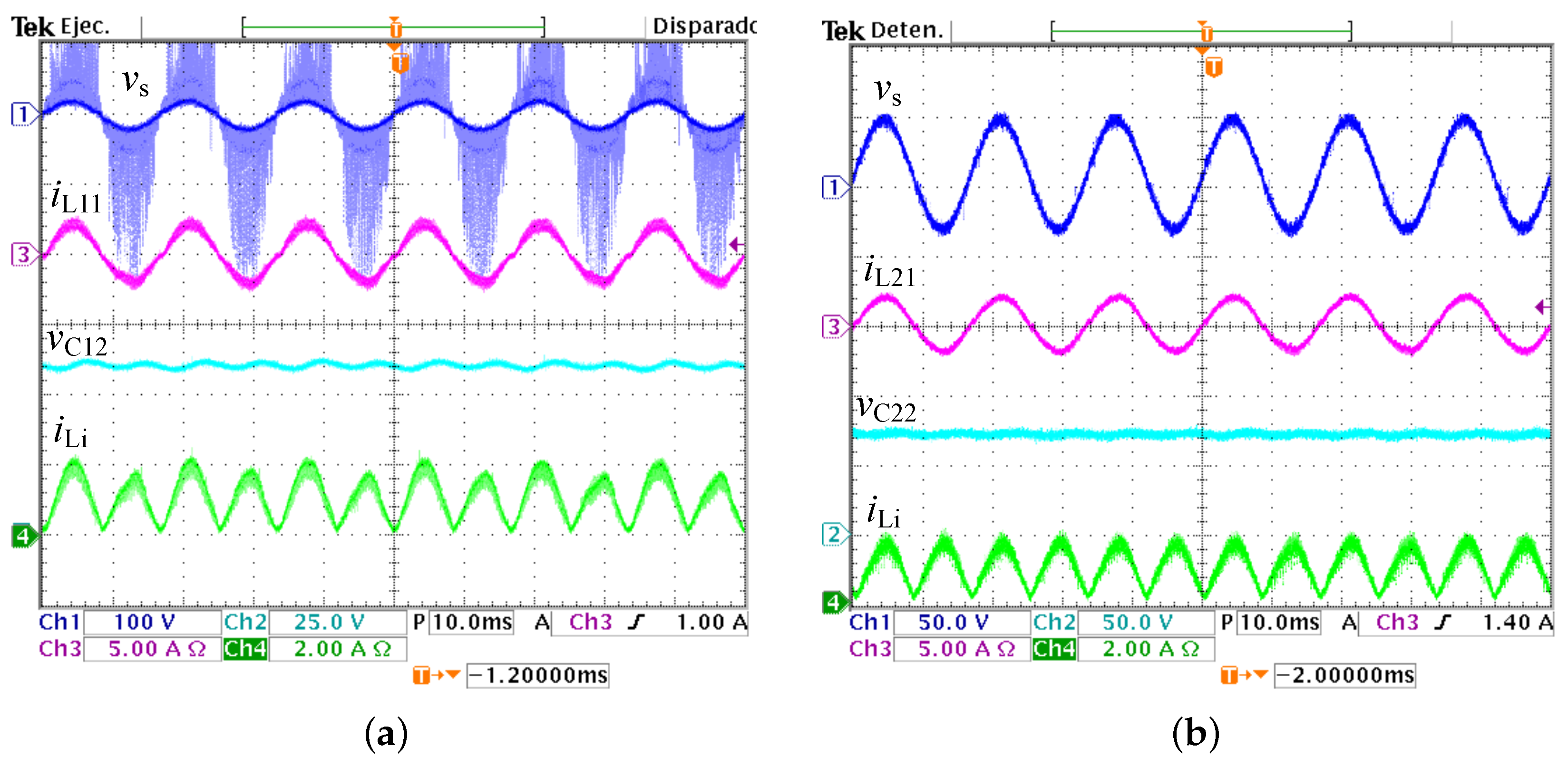
Figure 13 presents, from top to bottom, the input voltage v S , input current i L i c , output voltage v 0 , and inductor current i L i c of the SISUC-PFC with L and L C L filters. In particular, Figure 13a illustrates the steady-state response of the SISUC-PFC when an L filter is employed. As observed, the grid voltage and grid current are in phase, demonstrating appropriate power factor correction performance. Under these conditions, the input current exhibits a THD of 0.759%, which is obtained through the fast Fourier transform (FFT) of the current signals acquired using the Tektronix MSO 3034 (Tektronix, Inc., Beaverton, OR, USA) oscilloscope and the current probes TCP202A. This approach provides a more accurate estimation under the experimental conditions, particularly considering the low current levels involved. Additionally, note that the output voltage is observed to converge to the reference value, which confirms that the proposed controller satisfactorily fulfills the output voltage regulation objective. On the other hand, the inductor current i L i exhibits a full-wave rectified waveform as a direct consequence of the AC-DC rectification process. As a result, the output voltage of the DC–DC stage contains a low-frequency ripple at 120 Hz.
In Figure 13b, the steady-state response of the SISUC-PFC using an L C L filter is presented. As observed, the grid voltage and grid current are in phase. In this case, the grid current exhibits a THD of 0.203%, which is lower than that obtained when an L filter is employed. Similarly, the inductor current i L i exhibits a full-wave rectified waveform. It is worth noting that the use of an L C L filter at the rectifier input provides significant advantages compared to an L filter, since it offers higher attenuation of switching harmonics, resulting in a reduction in both the harmonic content and the ripple of the grid current. Furthermore, the higher attenuation provided by the L C L filter contributes to a reduction in the output voltage ripple, particularly the ripple associated with the rectification process. As a consequence, the value of the output capacitance can be reduced while maintaining the same voltage ripple level compared to the use of an L filter.
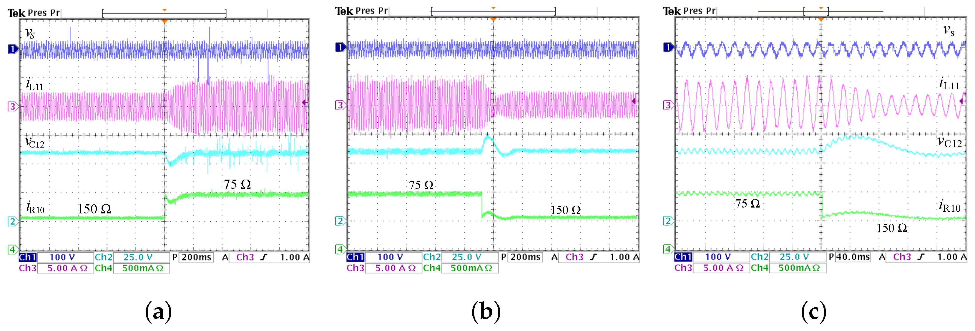
The transient responses of the grid voltage and grid current, as well as the output voltage and output current, are presented in Figure 14 and Figure 15 for different load conditions of the SISUC-PFC employing L and L C L input filters. In particular, Figure 14a–c illustrates the transient behavior associated with a load variation from 150 Ω to 75 Ω and back. The results show that the output voltage remains well regulated under load variations, confirming the effectiveness of the proposed controller. Moreover, the amplitudes of both the grid current and the output current are observed to increase proportionally with the load variation, as expected. Specifically, as shown in Figure 14c, the grid current preserves a sinusoidal waveform in phase with the grid voltage, demonstrating that power factor correction is maintained even under load variations.
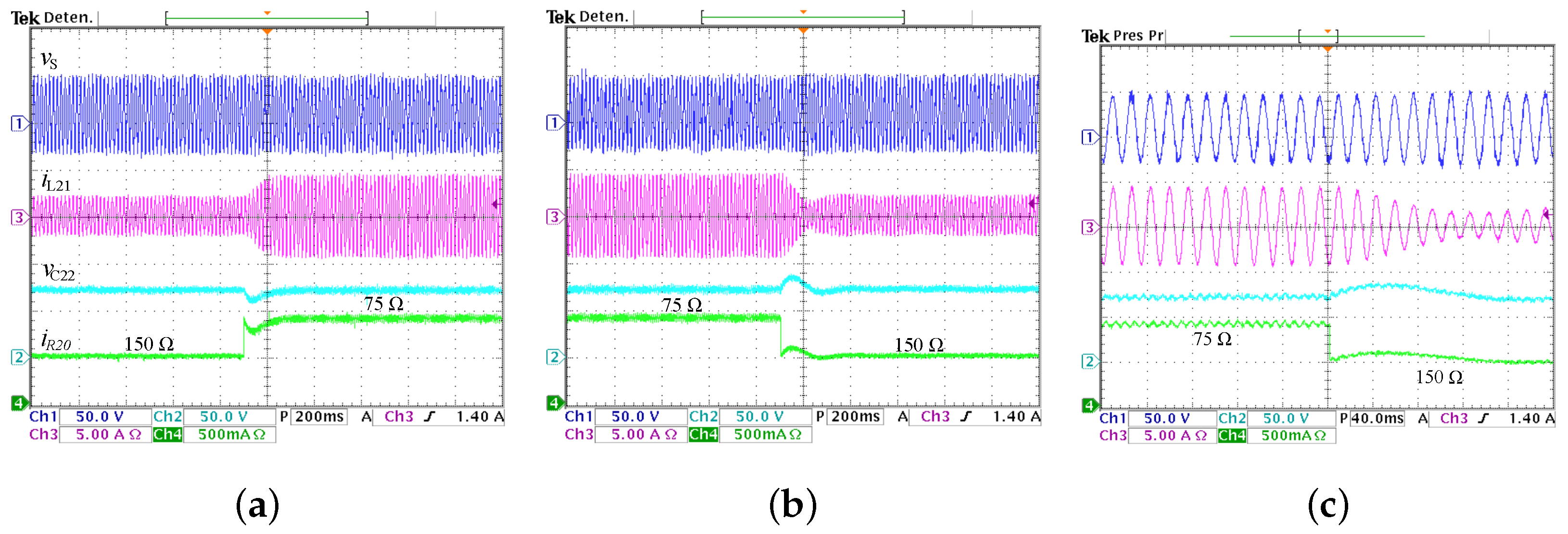
Figure 15 illustrates, from top to bottom, the transient responses of the grid voltage, grid current, output voltage, and output current of the SISUC-PFC with an L C L filter under load variations. The reference voltage is set to 75 V, while the load is changed from 150 Ω to 75 Ω and back. As shown in Figure 15a,c, output voltage regulation is achieved despite the load changes, although a voltage overshoot is observed during the load transitions. Subsequently, the output voltage converges to the reference value. Moreover, due to the use of the L C L filter, reduced noise is exhibited in the voltage and current waveforms compared to those obtained when an L filter is employed. Similarly, as shown in Figure 15c, a sinusoidal grid current with low harmonic content is preserved and remains in phase with the grid voltage, demonstrating that power factor correction is maintained even under load variations.
The experimental results show a behavior very similar to that obtained through numerical simulations. As can be observed, the output voltage and input current exhibit comparable dynamic responses and steady-state performance. In addition, both the transient response and the waveform profiles show strong agreement, with only minor discrepancies mainly attributed to non-ideal effects in the experimental implementation. These results validate the accuracy of the proposed model and the effectiveness of the control strategy, demonstrating a close correspondence between simulation and experimental results.

4.3. Efficiency Analysis

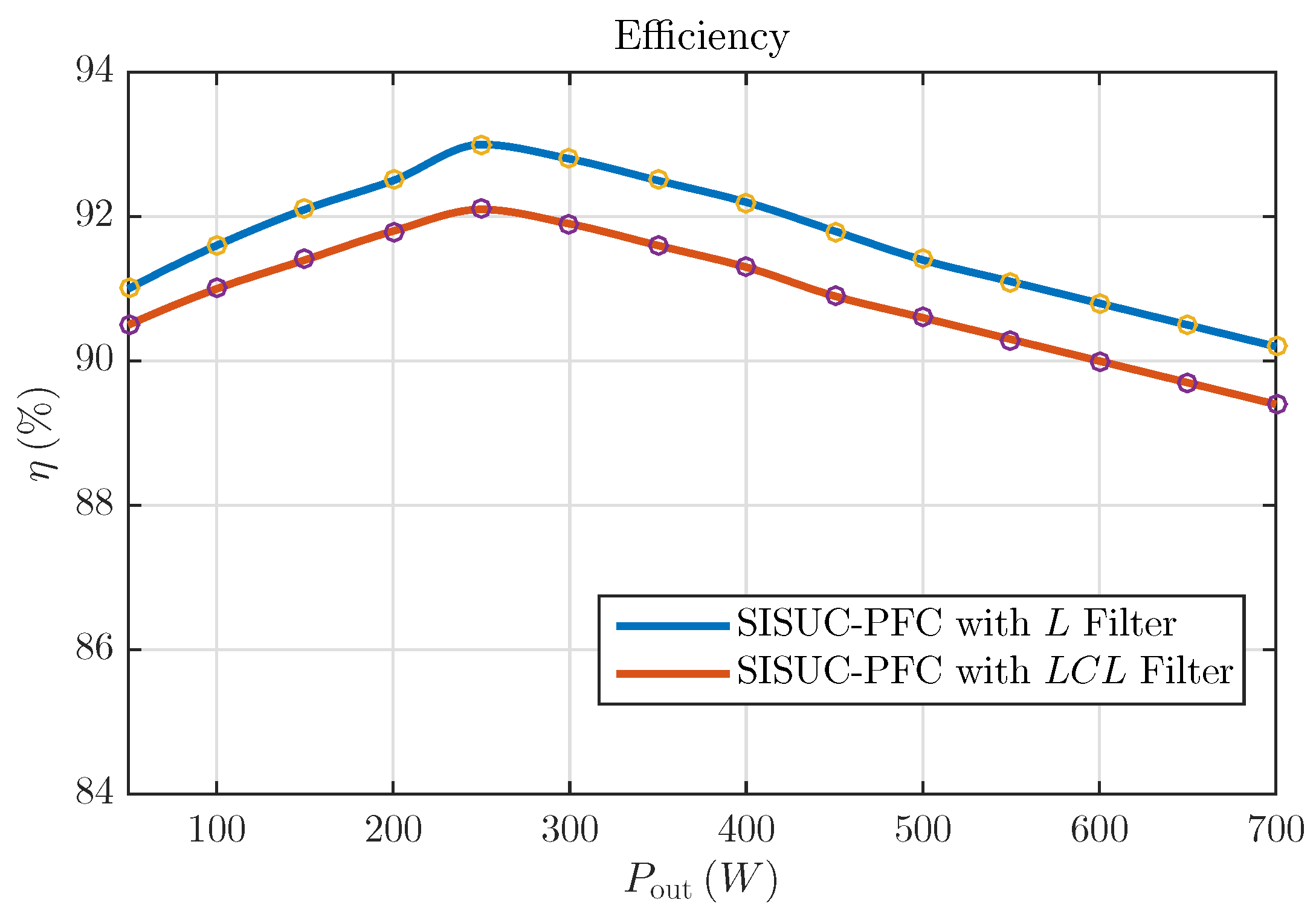
In this subsection, the efficiency analysis of the proposed systems is presented. For this purpose, the parasitic resistances of both semiconductor and passive components are considered based on the manufacturers’ datasheets. The efficiency is evaluated following the methodology described in [37]. As shown in Figure 16, both systems exhibit similar efficiency levels; however, the configuration with the L filter achieves a slightly higher efficiency compared to the L C L filter. In particular, a maximum efficiency of 92.8% is obtained at 250 W for the L filter, whereas the L C L filter reaches approximately 91.9%.
In Table 2, the main performance metrics of the proposed systems are summarized. As can be observed, the SISUC-PFC system with an L C L filter exhibits improved power quality, achieving a higher PF and lower total THD compared to the L filter configuration. However, the system with an L filter attains a slightly higher efficiency. In addition, the L-filter-based system presents a higher current ripple level compared to the LCL configuration. Despite this, the LCL-based configuration is considered a more suitable option due to its superior PF and THD performance, as well as its reduced current ripple. It is worth mentioning that, although the efficiency of both systems is below 95%, it can be improved through an appropriate selection of the components.

5. Conclusions

This paper presents a high-gain AC–DC converter based on the switched-inductor technique, capable of achieving a high conversion ratio for power factor correction applications. The system consists of an AC–DC stage with an uncontrolled full-wave rectifier and a passive input filter, followed by a DC–DC stage that provides the high conversion ratio. Both L and L C L filters are considered to improve input current quality. The main contribution of this work is the development of the system model and the design of the control strategy. In particular, a model-based approach is used to derive the control design from the averaged system model, resulting in a structured control scheme that includes an inner current loop based on a proportional-resonant controller and an outer voltage loop based on a PI controller with a low-pass filter.
The proposed system and control scheme were validated using a laboratory prototype. The experimental results demonstrate adequate input current tracking and stable output voltage under load variations within the tested operating conditions. The system with an L C L input filter achieves improved current quality, with a power factor close to unity, reduced current ripple, and lower harmonic distortion compared to the L filter case, as well as lower output voltage ripple. Although the LCL configuration requires more passive components, the inductance and capacitance values are smaller, resulting in reduced overall size and cost. Both configurations use the same sensing scheme, indicating that the improved performance is achieved without increasing implementation complexity.
It is important to highlight that the experimental validation presented in this work is based on a low-power academic prototype designed as a proof of concept. Although the operating conditions differ significantly from those of practical Level 1/Level 2 on-board EV chargers, which represent one of the potential applications of this system, the obtained results can be extrapolated to higher-power applications, since the proposed modeling approach and control law exhibit consistent performance and are not inherently dependent on the power level. Therefore, with an appropriate selection of passive components, semiconductor devices, and proper thermal management, similar dynamic behavior and control performance can be expected at higher power levels, with the potential for further improvements in PF and THD. In future work, the performance of the proposed system will be validated under higher output power conditions through appropriate component selection and an improved experimental prototype design. Additionally, future research will address the control design, analysis, and experimental validation of isolated high-gain converter topologies, such as Flyback-derived systems, to further evaluate their suitability for this type of application.

Author Contributions

Conceptualization, C.J.R.-C. and P.R.M.-R.; methodology, C.J.R.-C., P.R.M.-R., D.L.-C. and C.J.R.-C.; software, C.J.R.-C. and J.A.V.-L.; validation, C.J.R.-C. and J.A.V.-L.; formal analysis, C.J.R.-C., P.R.M.-R., D.L.-C. and J.A.V.-L.; investigation, C.J.R.-C., P.R.M.-R., D.L.-C., J.A.V.-L., G.V.-G. and J.M.S.; resources, P.R.M.-R. and D.L.-C.; data curation, P.R.M.-R. and D.L.-C.; writing—original draft preparation, C.J.R.-C., P.R.M.-R., D.L.-C., J.A.V.-L., G.V.-G. and J.M.S.; writing—review and editing, C.J.R.-C., P.R.M.-R., D.L.-C., J.A.V.-L., G.V.-G. and J.M.S.; visualization, C.J.R.-C., P.R.M.-R., D.L.-C., J.A.V.-L., G.V.-G. and J.M.S.; supervision, C.J.R.-C. and P.R.M.-R.; project administration, P.R.M.-R. and D.L.-C.; funding acquisition, P.R.M.-R. and. D.L.-C. All authors have read and agreed to the published version of the manuscript.

Funding

This research received no external funding.

Institutional Review Board Statement

Not applicable.

Informed Consent Statement

Not applicable.

Data Availability Statement

The original contributions presented in this study are included in the article. Further inquiries can be directed to the corresponding author.

Conflicts of Interest

The authors declare no conflicts of interest.

Abbreviations

The following abbreviations are used in this manuscript:
ACAlternating current
DCDirect current
DC–ACDirect current to alternating current
FBRDfull-bridge diode rectifier
DC–DCDirect current to direct current
LInductive Filter
L C L Inductor–Capacitor–Inductor Filter
MOSFETMetal-oxide-semiconductor field-effect transistor
PFCPower Factor Correction
PIProportional-integral
PRProportional-Resonant
SCSwitched capacitor
SISwitched inductor
SISUC-PFCSwitched-Inductor Step-Up Converter

References

  1. Rajashekara, K. Present Status and Future Trends in Electric Vehicle Propulsion Technologies. IEEE J. Emerg. Sel. Top. Power Electron. 2013, 1, 3–10. [Google Scholar] [CrossRef]
  2. Sayed, S.S.; Massoud, A.M. Review on State-of-the-Art Unidirectional Non-Isolated Power Factor Correction Converters for Short-/Long-Distance Electric Vehicles. IEEE Access 2022, 10, 11308–11340. [Google Scholar] [CrossRef]
  3. Quiroga, A.; Bayona, J.; Espitia, H. Review of Converter Circuits with Power Factor Correction. Technologies 2025, 13, 221. [Google Scholar] [CrossRef]
  4. Adragna, C.; Bianco, A.; Gritti, G.; Sucameli, M. State-of-the-Art Power Factor Correction: An Industry Perspective. Encyclopedia 2024, 4, 1324–1354. [Google Scholar] [CrossRef]
  5. Cacciotto, F.; Torrisi, S.; Aiello, G.; Rizzo, S.A. A PFC Control Management to Improve the Efficiency of DC-DC Converters. Electronics 2025, 14, 538. [Google Scholar] [CrossRef]
  6. Tseng, S.Y.; Fan, J.H. Bridgeless Boost Converter with an Interleaving Manner for PFC Applications. Electronics 2021, 10, 296. [Google Scholar] [CrossRef]
  7. Wu, S.T.; Chen, F.Y.; Chien, M.C.; Wang, J.M.; Su, Y.Y. A Hybrid Control Scheme with Fast Transient and Low Harmonic for Boost PFC Converter. Electronics 2021, 10, 1848. [Google Scholar] [CrossRef]
  8. Botila, D.A.; Pop-Calimanu, I.M.; Lascu, D. Buck Converter with Cubic Static Conversion Ratio. Sensors 2024, 24, 696. [Google Scholar] [CrossRef]
  9. Vazquez-Guzman, G.; Rodriguez-Cortes, C.J.; Martinez-Rodriguez, P.R.; Sosa-Zuniga, J.M.; Langarica-Cordoba, D.; Malinowski, M.; Stevens-Navarro, E. Design of a Step-Down Non-Isolated DC-DC n-Cell Converter with a High Reduction Ratio. IEEE Access 2024, 12, 126601–126610. [Google Scholar] [CrossRef]
  10. Monteiro, J.; Pires, V.F.; Foito, D.; Cordeiro, A.; Silva, J.F.; Pinto, S. A Buck-Boost Converter with Extended Duty-Cycle Range in the Buck Voltage Region for Renewable Energy Sources. Electronics 2023, 12, 584. [Google Scholar] [CrossRef]
  11. Abdel-Rahim, O.; Chub, A.; Blinov, A.; Vinnikov, D.; Peftitsis, D. An Efficient Non-Inverting Buck-Boost Converter with Improved Step Up/Down Ability. Energies 2022, 15, 4550. [Google Scholar] [CrossRef]
  12. Dimitrov, B.; Krishna, M.; Cruden, A.; Sharkh, S.; Elkhateb, A. Analysis, Design, and Experimental Validation of a Primary Side Current-Sensing Flyback Converter for Use in a Battery Management System. Electronics 2018, 7, 43. [Google Scholar] [CrossRef]
  13. Tseng, S.Y.; Fan, J.H. Buck-Boost/Flyback Hybrid Converter for Solar Power System Applications. Electronics 2021, 10, 414. [Google Scholar] [CrossRef]
  14. Kumar, G.K.N.; Verma, A.K.; N, S.; Shukla, K. A Single-Stage Boost Derived Switched-Capacitor- Based PFC Converter for EV Applications. IEEE J. Emerg. Sel. Top. Ind. Electron. 2024, 5, 225–233. [Google Scholar] [CrossRef]
  15. Soares, J.W.M.; Badin, A.A. High-Efficiency Interleaved Totem-Pole PFC Converter with Voltage Follower Characteristics. IEEE J. Emerg. Sel. Top. Power Electron. 2023, 11, 1879–1887. [Google Scholar] [CrossRef]
  16. Le, T.T.; Lee, J.; Choi, S. Single-Stage Totem-Pole AC–DC Converter Based on Boost Half-Bridge Structure for Battery Chargers. IEEE Trans. Power Electron. 2024, 39, 1060–1073. [Google Scholar] [CrossRef]
  17. Dixit, A.; Pande, K.; Gangavarapu, S.; Rathore, A.K. DCM-Based Bridgeless PFC Converter for EV Charging Application. IEEE J. Emerg. Sel. Top. Ind. Electron. 2020, 1, 57–66. [Google Scholar] [CrossRef]
  18. Musavi, F.; Eberle, W.; Dunford, W.G. A High-Performance Single-Phase Bridgeless Interleaved PFC Converter for Plug-in Hybrid Electric Vehicle Battery Chargers. IEEE Trans. Ind. Appl. 2011, 47, 1833–1843. [Google Scholar] [CrossRef]
  19. Singh, A.K.; Mishra, A.K.; Gupta, K.K.; Kim, T. Comprehensive review of nonisolated bridgeless power factor converter topologies. IET Circuits Devices Syst. 2021, 15, 197–208. [Google Scholar] [CrossRef]
  20. Ahmed, H.F.; Lahooti Eshkevari, A.; Abdoli, I.; Jamil, M. A Bridgeless Cuk AC–DC Converter with Improved Efficiency and Uniform Current Stress Sharing. IEEE Trans. Power Electron. 2026, 41, 5510–5521. [Google Scholar] [CrossRef]
  21. Han, J.K. Efficiency and PF Improving Techniques with a Digital Control for Totem-Pole Bridgeless CRM Boost PFC Converters. Energies 2024, 17, 369. [Google Scholar] [CrossRef]
  22. Gupta, S.; Vethanayagam, V.K.; Anbalagan, K. Reconfigurable Three-Leg Interleaved Totem-Pole PFC Converter with SPDT Relay for Optimized Light-Load Performance in EV Chargers. IEEE J. Emerg. Sel. Top. Power Electron. 2025, 13, 6909–6922. [Google Scholar] [CrossRef]
  23. Su, B.; Lu, Z. An Interleaved Totem-Pole Boost Bridgeless Rectifier with Reduced Reverse-Recovery Problems For Power Factor Correction. IEEE Trans. Power Electron. 2010, 25, 1406–1415. [Google Scholar] [CrossRef]
  24. Koh, H.G.; Ko, H.J.; Choi, Y.J. A MPCC-Based Variable Sampling Time Interleaving Method for a Two-Phase Totem-Pole Bridgeless Boost PFC Converter. IEEE Access 2023, 11, 104295–104304. [Google Scholar] [CrossRef]
  25. Tausif, A.; Bakan, A.F.; Dusmez, S. A High Power Density Zero-Voltage-Switching Totem-Pole Power Factor Correction Converter. IEEE Trans. Power Electron. 2024, 39, 837–849. [Google Scholar] [CrossRef]
  26. He, H.; Zhang, D.; Zhou, A.; Zhang, F.; Zou, X.; Yuan, J.; Wei, M. Virtual Admittance Feedforward Compensation and Phase Correction for Average-Current-Mode-Controlled Totem-Pole PFC Converters. Appl. Sci. 2023, 13, 9498. [Google Scholar] [CrossRef]
  27. Tsai, J.R.; Wu, T.F.; Wu, C.Y.; Chen, Y.M.; Lee, M.C. Interleaving Phase Shifters for Critical-Mode Boost PFC. IEEE Trans. Power Electron. 2008, 23, 1348–1357. [Google Scholar] [CrossRef]
  28. Xu, X.; Liu, W.; Huang, A.Q. Two-Phase Interleaved Critical Mode PFC Boost Converter with Closed Loop Interleaving Strategy. IEEE Trans. Power Electron. 2009, 24, 3003–3013. [Google Scholar] [CrossRef]
  29. Pradhan, R.; Keshmiri, N.; Emadi, A. On-Board Chargers for High-Voltage Electric Vehicle Powertrains: Future Trends and Challenges. IEEE Open J. Power Electron. 2023, 4, 189–207. [Google Scholar] [CrossRef]
  30. Acharige, S.S.G.; Haque, M.E.; Arif, M.T.; Hosseinzadeh, N.; Hasan, K.N.; Oo, A.M.T. Review of Electric Vehicle Charging Technologies, Standards, Architectures, and Converter Configurations. IEEE Access 2023, 11, 41218–41255. [Google Scholar] [CrossRef]
  31. Salmon, J. Circuit topologies for single-phase voltage-doubler boost rectifiers. IEEE Trans. Power Electron. 1993, 8, 521–529. [Google Scholar] [CrossRef]
  32. Jang, Y.; Jovanovic, M.M. Interleaved Boost Converter with Intrinsic Voltage-Doubler Characteristic for Universal-Line PFC Front End. IEEE Trans. Power Electron. 2007, 22, 1394–1401. [Google Scholar] [CrossRef]
  33. Guimarães, J.C.; Cortez, D.F.; Badin, A.A. Single-Phase Hybrid Switched-Capacitor Interleaved AC-DC Boost Converter. IEEE Access 2021, 9, 140799–140808. [Google Scholar] [CrossRef]
  34. Costa, P.J.S.; Illa Font, C.H.; Lazzarin, T.B. Single-Phase Hybrid Switched-Capacitor Voltage-Doubler SEPIC PFC Rectifiers. IEEE Trans. Power Electron. 2018, 33, 5118–5130. [Google Scholar] [CrossRef]
  35. Cortez, D.F.; Barbi, I. A Family of High-Voltage Gain Single-Phase Hybrid Switched-Capacitor PFC Rectifiers. IEEE Trans. Power Electron. 2015, 30, 4189–4198. [Google Scholar] [CrossRef]
  36. Diwakar Naik, M.; Vinatha, U. A Novel Single-Switch High-Gain DC–DC Converter with Active Switched Inductor. IEEE Trans. Circuits Syst. II Express Briefs 2024, 71, 4581–4585. [Google Scholar] [CrossRef]
  37. Rodriguez-Cortes, C.J.; Martinez-Rodriguez, P.R.; Langarica-Cordoba, D.; Rolan-Blanco, A.; Vazquez-Guzman, G.; Villanueva-Loredo, J.A.; Sosa, J.M. Design and Control of a Modular High-Gain DC–DC Converter with Extensible Switched-Inductor Cells. Electronics 2026, 15, 897. [Google Scholar] [CrossRef]
  38. Beres, R.N.; Wang, X.; Blaabjerg, F.; Liserre, M.; Bak, C.L. Optimal Design of High-Order Passive-Damped Filters for Grid-Connected Applications. IEEE Trans. Power Electron. 2016, 31, 2083–2098. [Google Scholar] [CrossRef]
  39. Levron, Y.; Kim, H.; Erickson, R.W. Design of EMI Filters Having Low Harmonic Distortion in High-Power-Factor Converters. IEEE Trans. Power Electron. 2014, 29, 3403–3413. [Google Scholar] [CrossRef]
  40. Sufyan, A.; Jamil, M.; Ghafoor, S.; Awais, Q.; Ahmad, H.A.; Khan, A.A.; Abouobaida, H. A Robust Nonlinear Sliding Mode Controller for a Three-Phase Grid-Connected Inverter with an LCL Filter. Energies 2022, 15, 9428. [Google Scholar] [CrossRef]
  41. Zhang, R.; Dong, J.; Wang, L.; Ma, W.; Yin, G. Stabilizing the Boost PFC Converter with a Time Delay Feedback Controller. Electronics 2023, 12, 2291. [Google Scholar] [CrossRef]
  42. Lee, G.Y.; Park, H.C.; Ji, M.W.; Kim, R.Y. Digitalized Control Algorithm of Bridgeless Totem-Pole PFC with a Simple Control Structure Based on the Phase Angle. Electronics 2023, 12, 4449. [Google Scholar] [CrossRef]
Figure 1. Conventional EV charging station for Level 1 and Level 2 on-board charger configurations.
Technologies 14 00314 g001
Figure 2. SISUC-PFC topology for power factor correction.
Technologies 14 00314 g002
Figure 3. Block diagram of the overall control scheme for the SISUC-PFC system with an L filter.
Technologies 14 00314 g003
Figure 4. Block diagram of the overall control scheme for the SISUC-PFC system with an L C L filter.
Technologies 14 00314 g004
Figure 5. Steady-state responses of the grid voltage v s , the grid current i L c 1 , output voltage v C c 2 , and inductor current i L i : (a) using an L filter and (b) using an L C L filter in the SISUC-PFC converter.
Technologies 14 00314 g005
Figure 6. Transient responses of the grid voltage v s , the grid current i L 11 , output voltage v C 12 , and output current i R 10 of the proposed converter with an L filter under load changes from 150 Ω to 75 Ω , and 75 Ω to 150 Ω .
Technologies 14 00314 g006
Figure 7. Transient responses of the grid voltage v s , the grid current i L 21 , output voltage v C 22 , and output current i R 20 of the proposed converter with an L C L filter under load changes from 150 Ω to 75 Ω , and 75 Ω to 150 Ω .
Technologies 14 00314 g007
Figure 8. SISUC-PFC topology for power factor correction with L C L filter and non-linear load.
Technologies 14 00314 g008
Figure 9. Steady-state responses of the grid voltage v s , the grid current i L 21 , output voltage v C 22 , and inductor current i L i of SISUC-PFC converter with L C L filter and nonlinear load.
Technologies 14 00314 g009
Figure 10. Transient responses of the output voltage v C 22 , the grid current i L 21 , and output current i R 20 of SISUC-PFC converter with L C L filter with nonlinear load.
Technologies 14 00314 g010
Figure 11. Diagram of the experimental validation of the SISUC-PFC converter.
Technologies 14 00314 g011
Figure 12. Steady-state responses of the grid voltage v s and the grid current i L c 1 : (a) using an L filter and (b) using an L C L filter in the SISUC-PFC converter.
Technologies 14 00314 g012
Figure 13. Steady-state responses of the grid voltage v s , grid current i L c 1 , output voltage v c 2 , and inductor current i L i : (a) using an L filter and (b) using an L C L filter in the SISUC-PFC converter.
Technologies 14 00314 g013
Figure 14. Transient responses of the grid voltage v s , the grid current i L 11 , output voltage v C 12 , and output current i R 10 of the proposed converter with an L filter under load changes: (a) load step from 150 Ω to 75 Ω , (b) load step from 75 Ω to 150 Ω , and (c) zoomed-in response for the load step from 75 Ω to 150 Ω .
Technologies 14 00314 g014
Figure 15. Transient responses of the grid voltage v s , the grid current i L 21 , output voltage v C 22 , and output current i R 20 of the proposed converter with an L C L filter under load changes: (a) load step from 150 Ω to 75 Ω , (b) load step from 75 Ω to 150 Ω , and (c) zoomed-in response for the load step from 150 Ω to 75 Ω .
Technologies 14 00314 g015
Figure 16. Efficiency comparison of the proposed systems.
Technologies 14 00314 g016
Table 1. Experimental and Numerical parameters of SISUC PFC.
Parameters of the SISUC-PFCL FilterLCL Filter
Grid Voltage ( v S )24 V RMS 24 V RMS
Reference Voltage ( V r e f c )75 V75 V
Switching Frequency ( f s w )10 kHz10 kHz
Inductor ( L c 1 , L c 2 , L i )1 mH, –, 2 mH1 mH, 2 mH, 2 mH
Capacitor ( C 11 )10  μ F
Output Capacitor ( C 0 )680  μ F680  μ F
Control LoopValueValue
Rectifier-side current tracking K p , i 1 = 20 K p , i 2 = 16
Voltage proportional gain K p , v 1 = 1.3 K p , v 2 = 1.7
Voltage integral gain K i , v 1 = 0.3 K i , v 2 = 0.4
Note: “–” indicates that the entry is not applicable.
Table 2. Comparison of the main performance metrics of the proposed SISUC-PFC converter using L and L C L filters.
MetricsSISUC-PFC with L FilterSISUC-PFC with LCL Filter
Power Factor ( P F )0.90.99
T H D i c n 0.759%0.203%
Efficiency ( η )92.8%91.9%
Current ripple ( Δ i 11 , Δ i 21 )HighLow
Disclaimer/Publisher’s Note: The statements, opinions and data contained in all publications are solely those of the individual author(s) and contributor(s) and not of MDPI and/or the editor(s). MDPI and/or the editor(s) disclaim responsibility for any injury to people or property resulting from any ideas, methods, instructions or products referred to in the content.