
Article

A Novel FEC Implementation for VSAT Terminals Using High-Level Synthesis

by
Najmeh Khosroshahi
1,2,*,
Ron Mankarious
2 and
Mohammad Reza Soleymani
1
1
Department of Electrical and Computer Engineering, Concordia University, Montreal, QC H3G 1M8, Canada
2
PolarSat Inc., Montreal, QC H8T 3J8, Canada
*
Author to whom correspondence should be addressed.
Aerospace 2026, 13(2), 155; https://doi.org/10.3390/aerospace13020155
Submission received: 9 January 2026 / Revised: 28 January 2026 / Accepted: 30 January 2026 / Published: 6 February 2026
(This article belongs to the Special Issue Advanced Satellite Communications for Engineers and Scientists)

Abstract

This paper presents a hardware-efficient field-programmable gate array (FPGA) implementation of a layered two-dimensional corrected normalized min-sum (2D-CNMS) decoder for quasi-cyclic low-density parity-check (QC-LDPC) codes in very small aperture terminal (VSAT) satellite communication systems. The decoder is described in C++ and synthesized using the Xilinx Vitis high-level synthesis (HLS) 2025 (AMD Xilinx, San Jose, CA, USA) tool, and then packaged and integrated as an intellectual property (IP) core within the Vivado Design Suite 2024 (AMD Xilinx, San Jose, CA, USA), enabling rapid prototyping and portability across FPGA platforms. Unlike conventional normalized min-sum (NMS) and two-dimensional normalized min-sum (2D-NMS) architectures, the proposed 2D-CNMS scheme employs dyadic, multiplier-free normalization combined with two-level magnitude correction, achieving near sum-product performance with reduced complexity and latency. The design is implemented on a Zynq UltraScale+ multiprocessor system-on-chip (MPSoC) (AMD Xilinx, San Jose, CA, USA) and supports real-time operation with a throughput of 29–41 Mbps at 100 MHz, while using only 9.6–22.4 k look-up tables (LUTs), 2.1–5.9 k flip-flops (FFs), and no digital signal processing (DSP) slices or block random-access memories (BRAMs). Bit-error-rate (BER) simulations over an additive white Gaussian noise (AWGN) channel show no error floor down to 10 8 . These results demonstrate that the proposed HLS-based 2D-CNMS IP core provides a resource-efficient, high-performance LDPC decoding solution as compared with existing LDPC implementation approaches. This LDPC solution targets performance enhancement in wireless communication systems and has been deployed on a multi-frequency time-division multiple-access (MF-TDMA) satellite link to assess its overall behavior, demonstrating improved performance with reduced resource usage.

1. Introduction

Hubless full-mesh very small aperture terminal (VSAT) communication systems are increasingly adopted in satellite networks for their resilience against single points of failure, support for direct VSAT-to-VSAT connectivity, and enhanced security through private network isolation [1]. Unlike traditional star-configured VSAT architectures that rely on a central hub, hubless full-mesh systems eliminate hub dependency and enable direct remote-to-remote communication, which is critical for modern satellite applications, such as broadband connectivity, Internet of Things (IoT) backhaul, and emergency communications. Reliable satellite communication requires robust forward error correction (FEC) to mitigate noisy channel conditions and maintain data integrity. Conventional FEC schemes such as turbo product codes (TPCs) [2], convolutional codes [3,4,5,6], and Reed–Solomon (RS) codes [3,4,7] have been widely deployed. However, low-density parity-check (LDPC) codes, and particularly quasi-cyclic LDPC (QC-LDPC) codes, have gained prominence due to their superior error-correction capability and hardware efficiency. QC-LDPC codes exploit structural regularity in the parity-check matrix, reducing memory and interconnect complexity while achieving near-optimal performance [8]. These advantages have led to their adoption in modern standards such as digital video broadcasting-satellite, second-generation (DVB-S2) [3], IEEE 802.11n (WiFi) [9], and fifth-generation (5G) new radio (NR) [10]. The sum-product (SP) algorithm, also known as belief propagation (BP) [11], remains the performance benchmark for LDPC decoding [12], but its probability-domain arithmetic is computationally expensive for resource-constrained field-programmable gate arrays (FPGAs). Simplified variants such as min-sum (MS) [13,14] and normalized min-sum (NMS) reduce complexity by replacing multiplications with add-compare-select operations, albeit at the cost of some coding gain. Further refinements, including second-minimum approximation min-sum (SAMS) [15], two-dimensional min-sum (2D-MS) [16], and two-dimensional normalized min-sum (2D-NMS) [11], improve accuracy with modest overhead. Traditional register-transfer-level (RTL)-based implementations of LDPC decoders are time-consuming, error-prone, and difficult to scale across evolving FPGA platforms. High-level synthesis (HLS) offers a modern design methodology that accelerates development, improves portability, and enables rapid design-space exploration without sacrificing hardware efficiency. For FPGA targets such as VSATPlus®, decoder micro-architecture strongly impacts throughput, latency, and power. Fully parallel layered designs achieve high per-iteration throughput but incur dense interconnect and tight timing closure [17]. Partially parallel designs reduce wiring and power at the cost of lower throughput [18], while pipelined block-serial decoders minimize area but increase latency [19]. Scheduling also influences convergence and memory organization: flooding requires more iterations and higher energy, whereas layered scheduling reduces iterations but demands careful memory banking [20,21]. Despite these advances, existing FPGA implementations struggle to balance error-correction performance, resource utilization, and power efficiency under stringent constraints typical of satellite systems. This gap motivates the need for an approach that combines algorithmic improvements with a scalable, hardware-aware design methodology leveraging HLS. To address this challenge, this work proposes a layered two-dimensional corrected normalized min-sum (2D-CNMS) decoder integrated into an HLS-based design flow for generating reusable LDPC intellectual property (IP) cores. The proposed architecture incorporates dyadic, multiplier-free normalization and dual scaling of the first and second minima, achieving near-SP performance while minimizing resource usage and power consumption.
The main contributions of this paper are as follows: (1) a hardware-aware LDPC decoder architecture based on the 2D-CNMS algorithm optimized for FPGA implementation; (2) an HLS-based design flow for generating reusable LDPC IP cores, reducing development complexity compared with traditional RTL approaches; and (3) comprehensive evaluation of post-implementation error-correction performance, resource utilization, and throughput under realistic satellite channel conditions. The remainder of this paper is organized as follows: Section 2 describes the VSATPlus system and its architectural constraints. Section 3 and Section 4 present the proposed LDPC decoder and algorithmic enhancements. Section 5 details the FPGA-oriented architecture. Section 7 reports simulation results and analyzes complexity-performance trade-offs. Finally, Section 8 concludes the paper and outlines future research directions.

2. VSATPlus® System Overview

The VSATPlus [22] system provides full-mesh, single-hop connectivity within a satellite network, leveraging multi-frequency time division multiple access (MF-TDMA) technology. Each terminal buffers user data and transmits it in short, high-speed bursts scheduled to avoid overlap, ensuring efficient satellite resource utilization without requiring a central hub for scheduling [23]. This hubless architecture supports diverse satellite applications, including broadband connectivity, IoT backhaul, emergency communications, and enterprise networking, where reliability and scalability are critical [23].
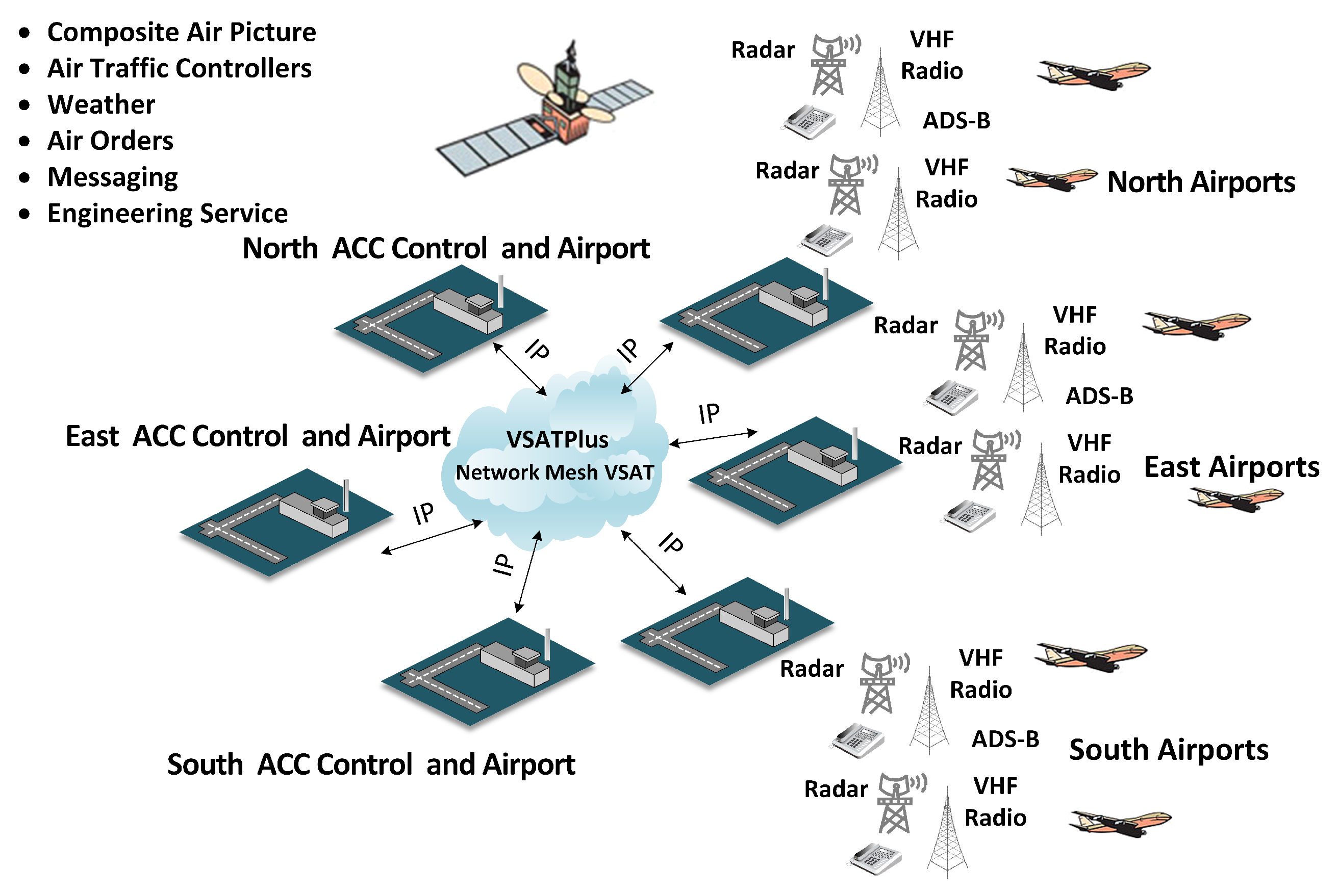
Figure 1 illustrates one example of VSATPlus deployment in air traffic control (ATC), showing direct Internet protocol (IP) connectivity between area control centers (ACCs) and airports across regions. The system supports radar, very high frequency (VHF) radio, automatic dependent surveillance-broadcast (ADS-B), and essential ATC services such as messaging, weather updates, and air traffic coordination. Similar principles apply to other mission-critical satellite services requiring secure, low-latency communication.
The VSATPlus modem is highly agile, capable of varying multiple parameters burst-by-burst. This flexibility enables carrier-to-carrier hopping for both transmit and receive over 32 carriers, along with adaptive modulation and FEC changes. This capability, referred to as Mesh-adaptive coding and modulation (ACM)TM, dynamically adjusts modulation and coding to accommodate different terminal antenna sizes and varying channel conditions across the network, optimizing throughput and reliability [23].
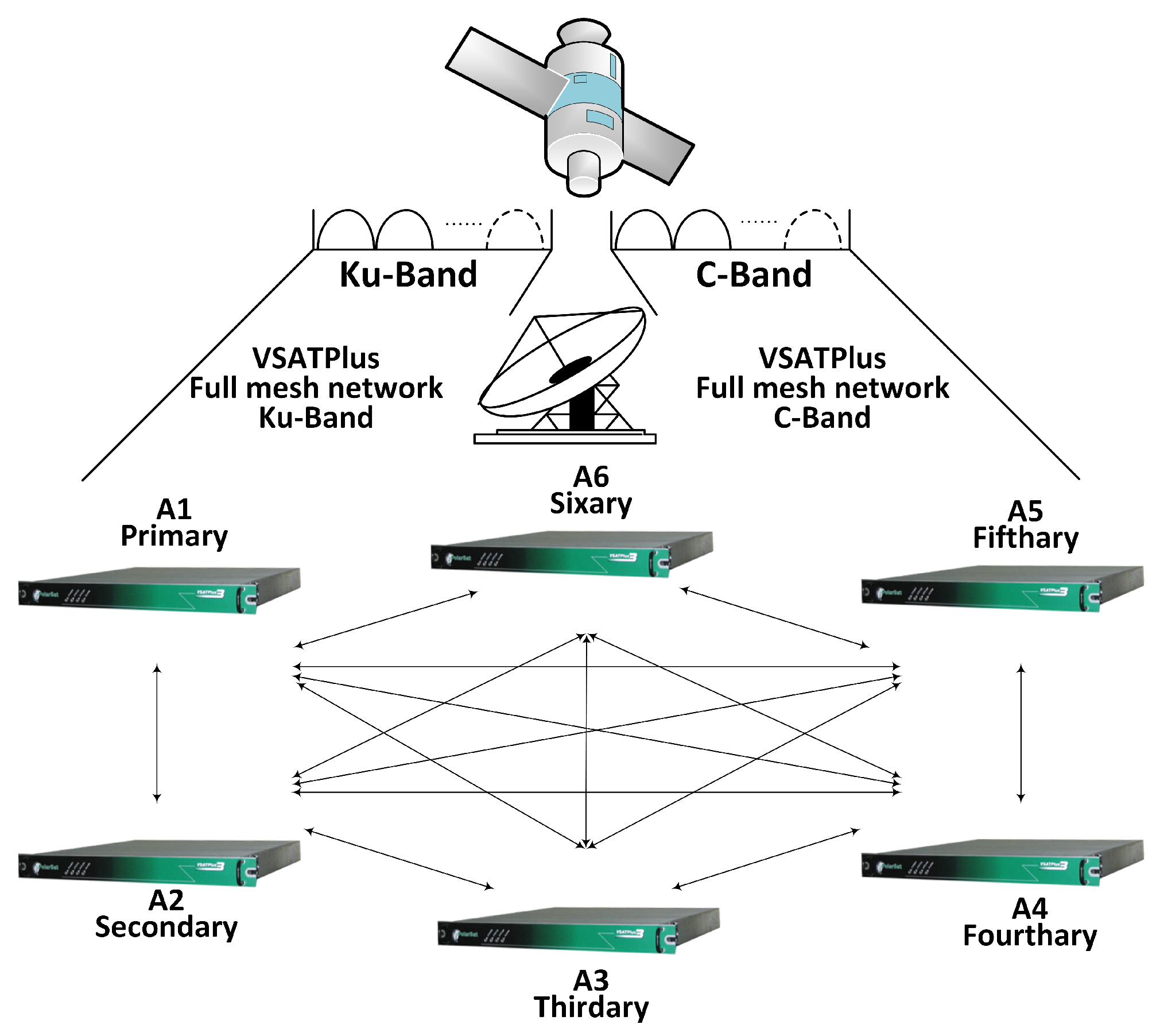
Figure 2 shows the architecture of a VSATPlus full-mesh, hubless network employing Ku-band and C-band satellite links for high-throughput communication. The satellite facilitates signal transmission from ground stations operating on both frequency bands, enabling simultaneous multi-band connectivity. The network consists of six nodes ( A 1 to A 6 ), interconnected in a full-mesh topology to ensure direct, bidirectional communication between all nodes. The labels (e.g., primary, secondary) indicate the logical roles or hierarchy of the nodes, while the consistent inter-node links. This architecture demonstrates the robustness and scalability of VSATPlus for distributed satellite applications beyond ATC, including broadband and enterprise networking.

3. Decoding Algorithmic Principles

QC-LDPC codes apply parity-check matrices tiled by Z × Z sub-matrices that are either circulant permutations of the identity or zeros [24]. This regular structure yields compact representations and lower memory requirements while enabling highly parallel, hardware-efficient decoders, an attractive performance/complexity trade-off for high-throughput satellite links. In satellite communication systems, where long propagation delays and limited link budgets make re-transmissions costly, efficient LDPC decoding is essential to maintain reliability and throughput. Although QC-LDPC codes may be degree-irregular (row and column weights ( d c , d v ) can vary), the locations of ones in H are deterministically specified by the permutation matrix and its circulant shifts, producing predictable, conflict-free access patterns rather than random placement [25]. Furthermore, the QC form organizes H as a regular array of blocks, with Z distinct memory banks for variable node data, enabling block-wise schedules that achieve scalable parallelism. A compressed permutation matrix, illustrated in Table 1, stores only shift offsets, where dash marks a zero block and non-negative entries specify the cyclic shift of the identity, minimizing footprint and simplifying decoder configuration. Owing to these advantages, QC-LDPC codes are widely adopted in modern communication standards.
The decoding of QC-LDPC codes typically employs SP algorithms, broadly classified by the type of message information exchanged during iterations. Hard-decision decoders, such as the bit-flipping (BF) algorithm, operate on binary decisions extracted directly from the channel [26], whereas soft-decision techniques, including the SP algorithm and its simplified MS variant, exploit soft information in the form of log-likelihood ratios (LLRs) [13,27]. These iterative message-passing algorithms exchange extrinsic information between variable nodes (VNs) and check nodes (CNs) over a bipartite graph representation of the parity-check matrix H, known as a Tanner graph [28], which underpins the inference mechanism that progressively refines the reliability of decoded bits across iterations.
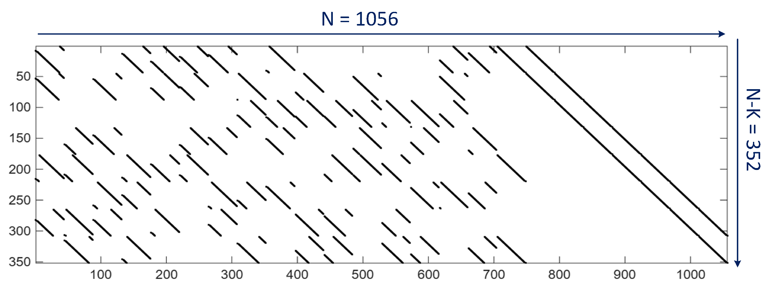
The structure of the LDPC parity-check matrix H used in this work is derived from the IEEE 802.16e (WiMAX) standard [29]. The matrix is constructed from a permutation matrix, shown in Table 1, composed of integer shift values and null entries, expanded by a lifting factor Z. The resulting H matrix is sparse and quasi-cyclic, as illustrated in Figure 3. Each diagonal or off-diagonal band in the figure corresponds to a circulant permutation matrix. Their distribution reflects the structured connectivity of VNs (columns) and CNs (rows).
Table 1. Permutation matrix of QC-LDPC code with R = 2 / 3  [30].
37--32192730-4-----213300------
36-35-2022-1-13-39--39--00-----
-------20171818297122---00----
-1732--1628-26--10-20-7---00---
512-72911----121130---0---00--
--623--41437----35226-----00-
27227-6-19--3633-22---------00
-38-7---33-2114-3315-250------0

3.1. Sum-Product (SP)/Belief Propagation (BP)

The SP/BP decoding algorithm initiates by calculating the LLRs for each received channel symbol r i at time i under an additive white Gaussian noise (AWGN) channel model, as follows:
L L R i = log Pr ( r i | t i = 1 ) Pr ( r i | t i = 1 ) = 2 r i σ 2 / 2
where σ 2 is the channel noise power following the Gaussian distribution. Initially, messages passed from the variable node v to the connected check node c are set to the LLR value derived from the received symbol, as given by
L v c = c M ( v ) c L c v
where c M ( v ) c represents the set of check nodes connected to the variable node v, excluding c. Next, the check node information is updated as follows:
L c v ( ) = 2 tanh 1 ( v N ( c ) v tanh L v c ( 1 ) 2 )
Once the convergence condition is satisfied or the maximum number of iterations is reached, the operation terminates. Subsequently, the hard decision for each variable node, v, is computed based on its LLR, as follows:
L v = L L R + c M ( v ) L c v
If L v 0 , then the estimated transmitted bit value is 0; otherwise, it is considered as 1.

3.2. Min-Sum (MS)

While SP achieves excellent error-correction performance, its reliance on nonlinear functions and probability-domain operations results in high computational complexity, motivating the development of simplified algorithms such as MS. The MS decoding algorithm simplifies the computational complexity of the SP algorithm by replacing nonlinear hyperbolic tangent functions with a minimum operation. Thus, the check node update equation simplifies to
L c v ( ) = ( v N ( c ) v sign ( L v c ( 1 ) ) ) min v N ( c ) v L v c ( 1 )
The variable nodes update, and hard decision processes remain consistent with the SP algorithm.

3.3. Normalized Min-Sum (NMS)

Although the MS significantly reduces hardware resource requirements and processing latency compared with the SP algorithm, it experiences degradation in bit-error-rate (BER) performance, typically around 0.5–1 dB [26]. This degradation primarily results from overestimation in extrinsic information exchange between nodes. To mitigate this effect, NMS applies a scaling factor, β ( 0 , 1 ) , to correct extrinsic information estimates, thereby enhancing practical decoding performance [31], as follows:
L c v ( ) = v N ( c ) v sign L v c ( 1 ) β min v N ( c ) v L v c ( 1 )
Whereas NMS attenuates the check-node minima by multiplying the raw minimum magnitude by a constant 0 < β < 1 , offset min-sum (OMS) instead applies a fixed subtraction to correct for the systematic overestimation introduced by the plain min-sum rule [32]. In OMS, each check-to-variable message is computed as
L c v ( ) = v N ( c ) v sign L v c ( 1 ) max min v N ( c ) v L v c ( 1 ) η , 0
where η > 0 is the offset parameter chosen to minimize the performance loss relative to the full belief-propagation algorithm [32]. Because the offset operation requires only a single subtraction per edge rather than a multiplication, OMS offers reduced critical-path latency and lower hardware resource usage compared with NMS.

3.4. Two-Dimensional Normalized Min-Sum (2D-NMS)

In the standard NMS algorithm, a single constant scaling factor compensates the overestimated magnitudes of all incoming check-to-variable messages. However, the extrinsic magnitude sent to a VN equals the smallest incoming magnitude, min 1 , for all edges except the edge, which uses the second-smallest incoming magnitude, min 2 , due to edge exclusion. Consequently, applying one scale for both cases can miscalibrate some messages and degrade performance. The 2D-NMS addresses this by applying distinct scaling ( β 1 , β 2 ), conditioned on whether min 1 or min 2 is used, yielding more accurate LLRs with only modest added complexity [33], as follows:
L c v ( ) = ( v N ( c ) v sign ( L v c ( 1 ) ) ) × β 2 × min 2 β 1 × min 1
For LDPC decoders employing the 2D-NMS algorithm, the optimal normalization factors ( β 1 , β 2 ) are predominantly determined by the check node degree ( d c ), which is determined by the parity check matrix.

3.5. Two-Dimensional Min-Sum (2D-MS)

While 2D-NMS compensates the check-node magnitude bias via the scaling pair ( β 1 , β 2 ), it applies the same gain to both message flows. Density-evolution analysis in [16] shows that the residual bias on the variable-to-check stream differs statistically from that on the check-to-variable stream. Therefore, introducing a second, direction-specific scaling pair eliminates this asymmetry and closes the remaining gap to SP decoding with only two extra multiplications per edge. To address this residual asymmetry more effectively, ref. [16] proposes applying iteration-dependent scale factors ( α ( ) , β ( ) ) directly to the extrinsic LLRs on each edge, resulting in
L ˜ v c ( ) = α ( ) L v c ( )
while the corresponding check-to-variable updates is as follows:
L ˜ c v ( ) = ( v N ( c ) v sign ( L ˜ v c ( 1 ) ) ) β ( ) min v N ( c ) v L ˜ v c ( 1 )
Although ( α ( ) , β ( ) ) can be optimized adaptively based on the code structure and channel SNR, [16] demonstrates that exhaustive AWGN profiling across the operational E b / N 0 range yields two fixed scale factors that preserve virtually all of the SP decoder’s extrinsic-information fidelity.

4. Two-Dimensional Corrected Normalized Min-Sum (2D-CNMS)

For VSATPlus terminals, even modest coding-gain improvements translate into reduced power-amplifier back-off and increased fade margins. However, the SP decoding algorithm remains computationally impractical for the throughput and power envelopes of the target FPGA platforms. Building on [16,33], we propose a 2D-CNMS decoder that preserves the add-compare-select arithmetic of MS while recovering a substantial fraction of the residual gap to an SP algorithm. The update introduces two shift-based per-edge scaling per iteration and incurs no additional on-chip memory, thereby maintaining low architectural complexity. Therefore, the scaled variable-to-check update is defined as
L ˜ v c ( ) = α ¯ L v c ( )
while the scaled check-to-variable update is given by
L ˜ c v ( ) = ( v N ( c ) v sign ( L ˜ v c ( 1 ) ) ) × β 2 ¯ × min 2 β 1 ¯ × min 1
Similar to a 2D-NMS algorithm, min 1 and min 2 denote the smallest and second-smallest absolute values of the incoming messages | L ˜ v c ( 1 ) | , where v N ( c ) v .

5. 2D-CNMS Hardware Implementation

Hand-optimized RTL design has traditionally been the standard approach for FPGA-based LDPC decoders. However, HLS methodologies [34] and commercial toolchains such as Vitis high-level synthesis (HLS) 2025 (AMD Xilinx, San Jose, CA, USA) [35] now offer a more productive alternative by enabling designers to specify the decoder in C/C++ or SystemC and automatically generate synthesizable RTL. In practice, HLS significantly reduces design and verification effort [36], while achieving area, timing, and power results comparable to expert-tuned hardware description language (HDL) implementations [36]. Furthermore, a single high-level source is portable across FPGA families and integrates seamlessly with the VSATPlus C-based simulation environment, facilitating rapid design-space exploration and system-level validation. Algorithm 1 summarizes the layered scheduling strategy employed in the proposed 2D-CNMS decoder. Compared with conventional layered MS, the proposed approach introduces a uniform variable-to-check scaling factor, α ¯ , and a two-level check-to-variable scaling pair ( β ¯ 1 , β ¯ 2 ), conditioned on whether the outgoing message is derived from min 1 or min 2 . These refinements improve extrinsic information accuracy while preserving the low-complexity arithmetic of MS.
Algorithm 1 Layered 2D-CNMS QC-LDPC Decoder
  1:
Kernel 1: Initialization
  2:
# Pipeline directive
  3:
Load LLR v ch into VN accumulator memory
  4:
Initialize message memory
  5:
Kernel 2: Process Decoding Iterations
  6:
while  i = 1 : Itr m a x  do
  7:
         Kernel 2.1: Compute VN Incoming Messages
  8:
         for  h = 1 : M / Z  do
  9:
                  # Pipeline directive
10:
                  for all check-nodes c in layer h do
11:
                           Load L v c ( i ) : v N ( c ) from VN–message RAM
12:
                           for all v N ( c ) do
13:
                                    # Unroll directive
14:
                                     sign ( L c v ( i ) ) = v N ( c ) v sign ( L v c ( i 1 ) )  
15:
                                     | L c v ( i ) | = β ¯ 1 × min 1 { v N ( c ) v } | L v c ( i 1 ) | β ¯ 2 × min 2 { v N ( c ) v } | L v c ( i 1 ) |
16:
                                    Write L c v ( i ) to CN–message RAM
17:
                           end for
18:
                  end for
19:
         end for
20:
         Kernel 2.2: Generate VN Output Messages
21:
         for  u = 1 : N / Z  do
22:
                  # Pipeline directive
23:
                  for all variable-node v in layer u do
24:
                           Load L c v ( i ) : c M ( v ) from CN–message RAM
25:
                           for all c M ( v ) do
26:
                                    # Unroll directive
27:
                                     L v c ( i ) = L v ( i 1 ) + α ¯ c M ( v ) c L c v ( i 1 )
28:
                                    Write L v c ( i ) to VN–message RAM
29:
                           end for
30:
                  end for
31:
         end for
32:
end while
33:
Kernel 3: Compute VNs Hard Decision
34:
for all  v = 1 : N  do
35:
         # Pipeline directive
36:
          c ^ v 0 if L v ( i ) < 0 else 1
37:
end for
38:
return Decoded Word, c ^ v
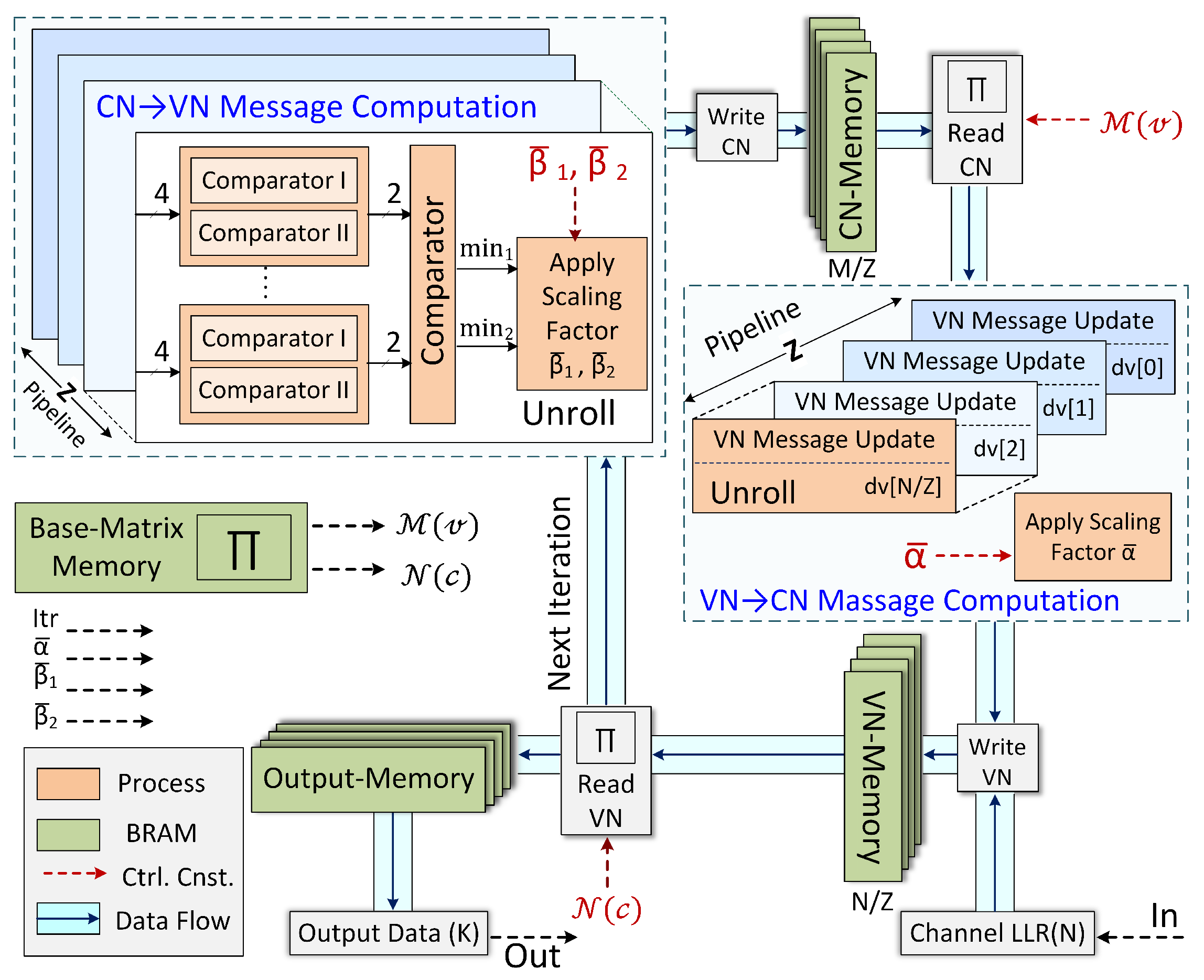
The proposed decoder is implemented using Vitis HLS 2025, leveraging loop-level parallelism and pipelining to maximize throughput. Inner loops responsible for CN and VN updates are partially or fully unrolled to generate multiple CN→VN and VN→CN messages per cycle, while outer loops are pipelined to minimize the initiation interval (II), enabling iteration overlap and reducing latency. The inherent layered structure of QC-LDPC codes facilitates deterministic memory banking and partitioning across Z independent memory banks implemented using distributed RAM and registers, supporting concurrent read-modify-write operations aligned with layer boundaries. Address generation is performed using two read-only memory (ROM)-based look-up tables (LUTs) precomputed from the base matrix: N ( c ) for CN updates and M ( v ) for VN updates. These index tables enable constant-time routing without additional buffering or pointer chasing, ensuring efficient memory access.
The HLS-based 2D-CNMS decoder architecture, illustrated in Figure 4, comprises two fully parallel processing engines: one dedicated to CN message computation and the other to VN message computation. Each engine interfaces directly with distributed random access memory (RAM) and registers under the control of a compact ROM storing non-negative cyclic-shift offsets and connection degrees derived from the base matrix.
In the CN engine, which comprises M / Z parallel pipelines, each pipeline retrieves a Z-wide vector of extrinsic LLRs from the VN RAM, applies a fixed-depth tree of four-input comparators to identify the smallest and second-smallest magnitudes, determines the overall output sign through a single XOR reduction stage, and adjusts these minima using normalization factors ( β ¯ 1 , β ¯ 2 ). The normalized extrinsic messages are then written back to the CN-RAM via the dual-port interface. Similarly, the VN engine, consisting of N / Z parallel pipelines, reads the updated CN messages along with the original channel LLRs, accumulates them using an adder tree, subtracts each corresponding extrinsic to form new messages, scales the result by α ¯ , applies eight-bit saturation, and generates provisional hard decisions based on the sign. Both the updated soft-value vectors and hard-decision bits are subsequently written to the VN RAM and output RAM, respectively.

6. End-to-End Vivado Design Suite 2024 Block Design

Figure 5 illustrates the integrated encoder-channel-decoder chain instantiated in Vivado 2024 (AMD Xilinx, San Jose, CA, USA), the Xilinx FPGA design and implementation platform, by introducing external IP cores generated using the Xilinx Vitis HLS 2025, high-level synthesis toolchain. Although the LDPC IP core was validated at a clock frequency of 350 MHz, the design employs a 100 MHz system clock generated by the clocking wizard IP and distributed via the processor system reset module. Each frame begins with a single-cycle start pulse, and all AXI4-Stream interfaces operate without backpressure, with the ready signal held asserted.
A pseudo-random source generates independent and identically distributed (i.i.d.) Bernoulli bits using a linear feedback shift register (LFSR) method. After AXI4-Stream handshakes, the QC-LDPC encoder accepts the payload and emits a serialized codeword. An RTL binary phase-shift keying (BPSK) modulator maps bits to signed 8-bit symbols with values { + 127 , 128 } . Additive noise is produced by an external AWGN IP implementing the Box–Muller transform (see Appendix C). Variance and seed registers are programmed via AXI4-Lite memory-mapped writes issued by the Zynq UltraScale+ multiprocessor system-on-chip (MPSoC) (AMD Xilinx, San Jose, CA, USA) processing system (PS), enabling deterministic initialization and run-time reconfiguration of the programmable logic (PL) core. The noise stream is buffered in a first-in first-out (FIFO) to decouple producer and consumer timing. On readout, the noise is added to the BPSK waveform, saturated to [ 128 , 127 ] , and treated as the input LLR stream for the decoder. Similar to AWGN parameters, the iteration limit, Itr max , is also configured by a control register for each frame.
During transmission, the reference bit for each payload position is stored in a reference FIFO. In parallel, a channel hard decision is derived from the sign of the saturated received sample and stored in a second FIFO to measure uncoded performance. When decoded bits become available, they are compared against the reference FIFO to accumulate the post-decoder error count, while the channel-hard stream is compared against the same reference to count bit flips caused by noise.

7. Emulation Results

We evaluate decoding algorithms under a layered schedule on the QC-LDPC code ( 1056 , 704 ) with Itr max = 50 using 8-bit fixed-point LLRs (clip/saturate) and syndrome-based early termination. The channel is AWGN, and E b / N 0 is swept on a uniform grid with sufficient frames per point to probe down to BER 10 8 . All baselines use identical quantization, stopping criteria, and layered scheduling for a fair comparison. Unlike conventional NMS, the proposed 2D-CNMS introduces dual-direction scaling and normalization refinements that significantly improve convergence speed and error-floor performance while maintaining FPGA-friendly complexity.
According to [33], the optimal two-level CN normalization factors ( β 1 , β 2 ) decrease with increasing check-node degree ( d c ) and approach constants at high SNR. Specifically, for the regular codes with d c = 6 and SNR [ 0 , 4 ] dB, β 1 [ 0.50 , 0.90 ] and β 2 [ 0.27 , 0.50 ] , trending toward the upper end as SNR rises. Consistently, [16] reports nearly iteration-invariant scalings for IEEE 802.11n ( 1944 , 1296 ) , R = 2 / 3 as α ¯ 0.9007 and β ¯ 0.8973 , achieving BER within 0.02 dB of an SP algorithm over E b / N 0 [ 1.4 , 2.6 ] dB. In line with [37], the strongest single-scalar NMS baseline uses a fixed normalization schedule, as follows:
β ( ) = 3 / 4 + 2 ( + 1 ) if 2 5 , else 3 / 4
where represents the number of iterations.
These observations support fixed, iteration-invariant gains. Guided by coarse-to-fine emulation sweeps on the target IEEE 802.16e QC-LDPC codes (rates 1 / 2 , 2 / 3 , 3 / 4 ), we therefore map ( β 1 , β 2 ) to β 1 ¯ = 0.8125 and β 2 ¯ = 0.875 , and set the VN gain to α ¯ = 0.75 . All scalings are implemented via shift-and-subtract to eliminate multipliers and extra memory.

7.1. Performance and Complexity Comparison

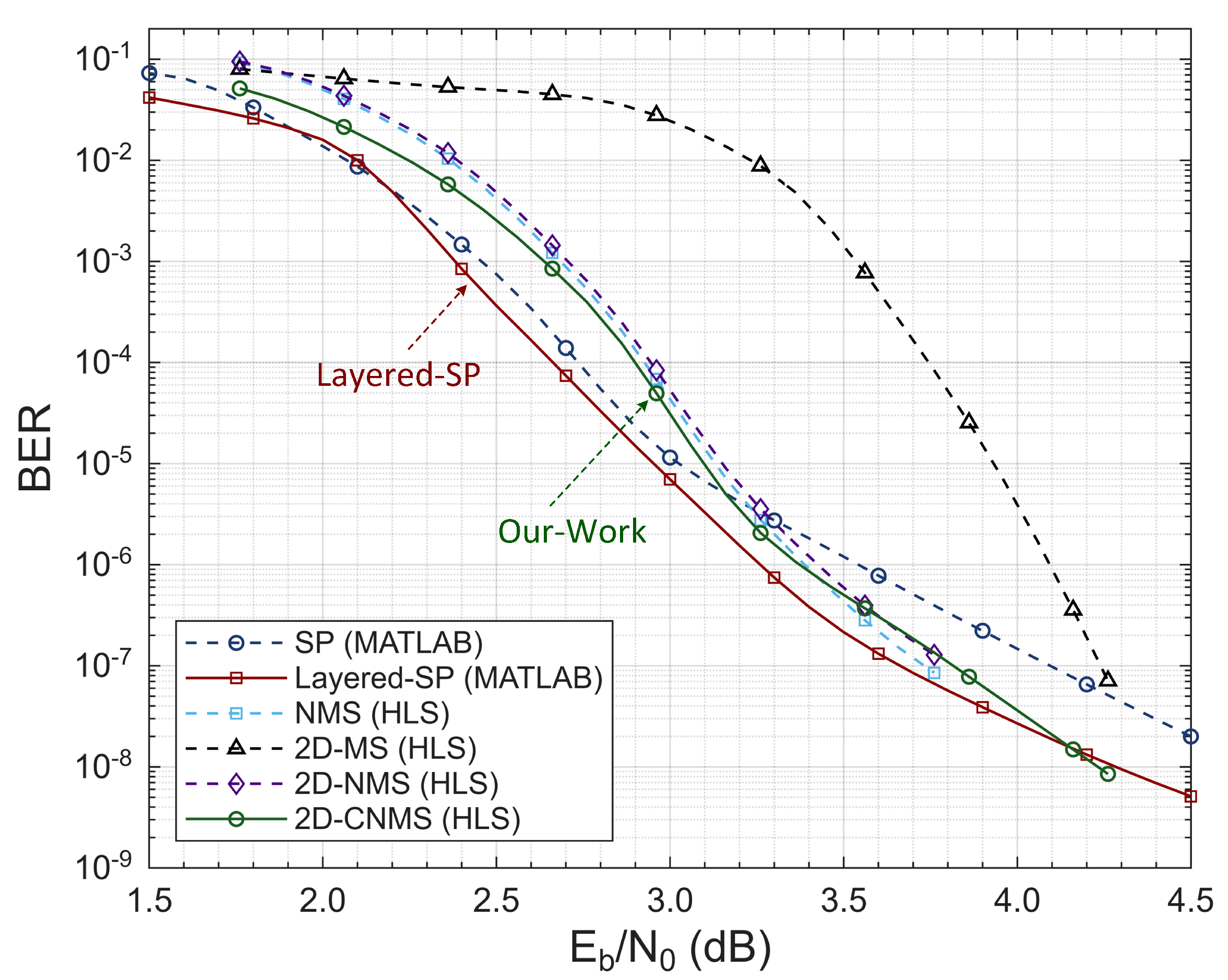
Figure 6 compares full-SP, layered-SP, NMS ( β = 0.75 ) [31,37], 2D-MS ( α ¯ = β ¯ 0.899 ) [26], 2D-NMS ( β 1 , β 2 ) = ( 0.75 , 0.875 ) [33], and the proposed 2D-CNMS ( α ¯ , β 1 ¯ , β 2 ¯ ) = ( 0.75 , 0.8125 , 0.875 ) on a QC-LDPC code ( 1056 , 704 ) with Itr m a x = 50 . Across the operational E b / N 0 range, a few algorithms, notably layered-SP and, at certain SNR points, 2D-NMS, exhibit slightly better BER performance than the proposed 2D-CNMS. This behavior is expected and is consistent with the algorithmic discussion in Section 3: layered-SP employs full message-passing scheduling with nonlinear message updates, whereas 2D-CNMS deliberately adopts MS style add-compare-select operations with dual shift-based normalization to remain multiplier-free and FPGA-efficient. The modest loss in BER therefore reflects a deliberate trade-off between decoding optimality and hardware realizability. At the same time, 2D-CNMS outperforms the other MS-based variants (NMS, 2D-MS, 2D-NMS) because the dual normalization ( α ¯ , β ¯ 1 , β ¯ 2 ) compensates for the residual gap to SP more effectively while avoiding multipliers and additional memory, yielding better BER in both the waterfall and high-SNR regions at substantially lower complexity and thus the most favorable performance-complexity trade-off.
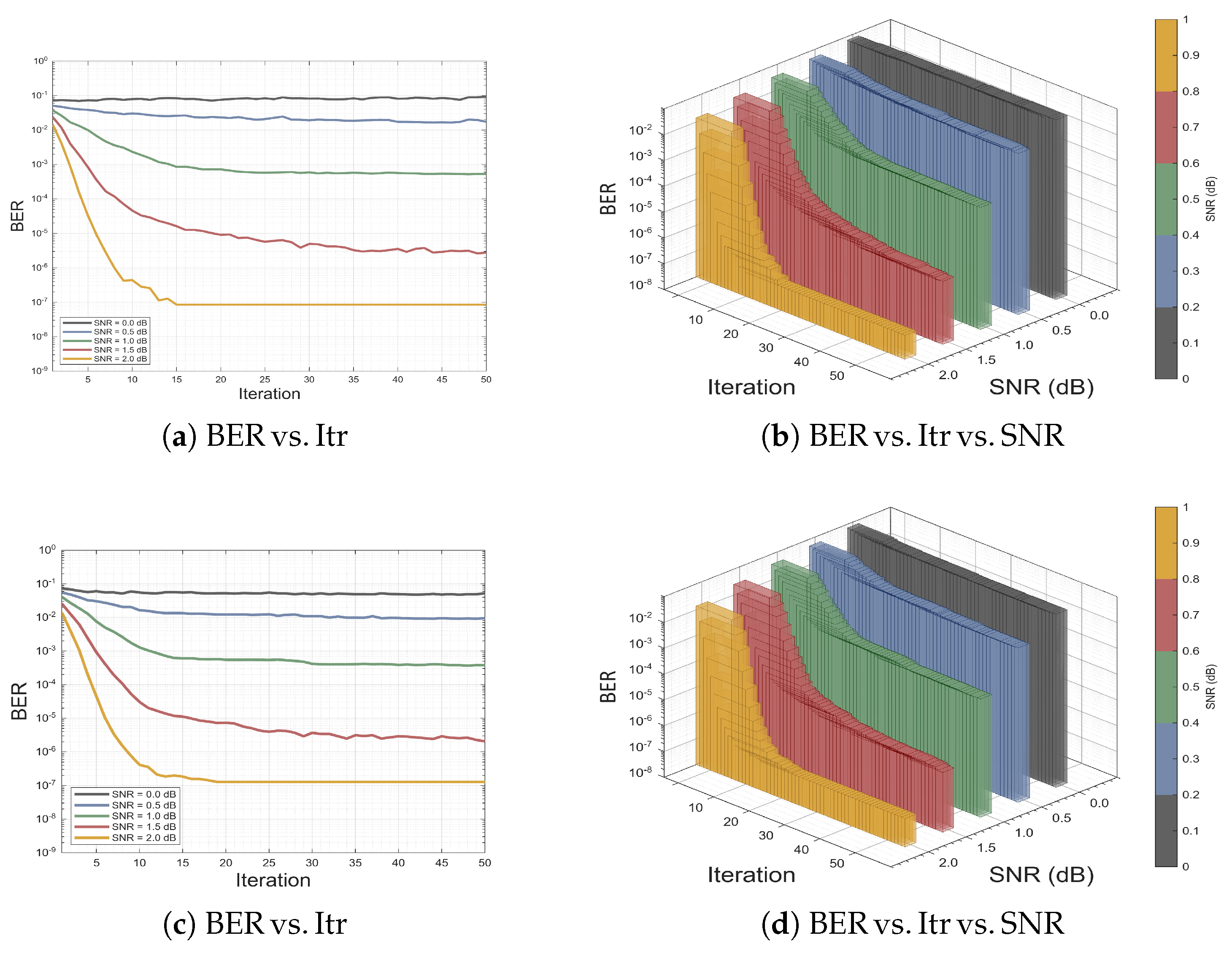
Figure 7 reports BER versus decoder iterations for the ( 1056 , 704 ) code under BPSK/AWGN. At SNR = 2.0 dB, the proposed 2D-CNMS achieves BER 10 7 by approximately 12 iterations, whereas the conventional NMS (with β = 0.75 ) requires roughly 15 iterations. For SNR 1.5 dB, neither method reaches 10 7 within 50 iterations. Nevertheless, 2D-CNMS maintains a uniformly lower BER for the same iteration budget and, at SNR = 1.5 dB, attains BER 10 6 in the mid-30s iterations, while NMS does not achieve 10 6 within 50 iterations. These iteration savings translate directly to reduced latency and higher throughput (see Section 7.3).
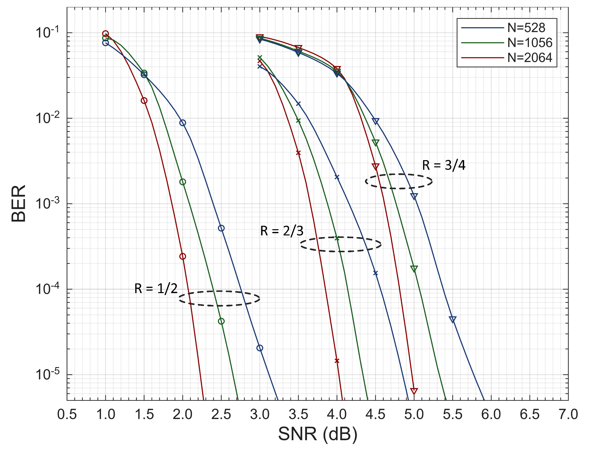
Figure 8 presents the BER performance of the proposed 2D-CNMS decoder for the IEEE 802.16 e QC-LDPC code profiles. For each code rate ( R = 1 / 2 , 2 / 3 , 3 / 4 ) , three block lengths ( N = 528 , 1056 , 2064 ) are shown. As expected, lower-rate codes achieve better BER at a given SNR, while higher-rate codes are shifted to the right. For a fixed rate, increasing the block length improves the coding gain, with longer codes exhibiting a steeper waterfall region over the simulated SNR range.
Table 2 contrasts the arithmetic requirements of SP, MS, NMS, OMS, 2D-MS, 2D-NMS, and the proposed 2D-CNMS on a per-check-node basis. SP demands d c multiplications and d c 1 divisions. 2D-MS retains two multipliers. In the proposed 2D-CNMS approach, we remove the multipliers and dividers and keep the comparator count d c + log 2 d c 2 .
Normalization is implemented using three subtractions, followed by a fixed power-of-two scaling corresponding to 12 right bit shifts. This 12-bit shift acts as a fixed-point approximation of the SP normalization factors, which require multiplications, in the 2D-CNMS algorithm for the considered IEEE 802.16e QC-LDPC codes. As confirmed by the decoding performance curves in Figure 6, this simple 12-bit shift achieves near-SP error-rate performance while completely avoiding multipliers and dividers. Consequently, the resulting data path is digital signal processing (DSP)-free and FPGA-native: 2D-CNMS, similar in spirit to OMS, NMS, 2D-MS, and 2D-NMS, trades multiplications/divisions for lightweight comparisons and shifts, delivering SP-like decoding behavior with significantly simpler hardware or, equivalently, better performance for a comparable hardware cost.

7.2. Resource Utilization

Table 3 summarizes representative LDPC decoder implementations on FPGA platforms for WiMAX [29], WiFi [9], and DVB-S2 [3] standards. Most of these designs target throughputs in the hundred-Mbps range, but at the cost of very large logic and memory footprints, typically on the order of 8.7–187 k LUTs and 3–1703 block random-access memories (BRAMs). These figures provide a reference envelope for conventional MS/OMS decoders implemented either via HLS or hand-tuned RTL.
The dominant resource bottleneck in LDPC decoding is often memory, because each iteration repeatedly reads and writes extrinsic messages while applying QC cyclic-shift permutations dictated by the rate-dependent permutation matrix. In a straightforward hardware mapping, these messages are typically stored in BRAM since multiple concurrent accesses are required per cycle. For highly parallel and irregular access patterns, BRAM replication may be inferred to emulate multi-port behavior, which can significantly increase BRAM usage, especially at higher code rates. In this work, each code rate uses a different permutation matrix [30], which changes the arrangement of non-empty circulant sub-matrices and shift distribution, thereby affecting connectivity and the “bank-friendliness” of the access schedule.
As highlighted in the gray-shaded rows at the bottom of Table 3, the proposed 2D-CNMS QC-LDPC decoder achieves comparable tens-of-Mbps throughput (29–34 Mbps at 100 MHz for WiMAX rate-1/2 codes) while using only 9.7 11.7 k LUTs and zero BRAM blocks. In contrast, many prior FPGA-based decoders require tens to hundreds of thousands of LUTs and from a few up to more than 1700 BRAM blocks to reach similar or higher throughput regimes. Thus, within the reference envelope established by Table 3, the proposed architecture provides a more favorable logic/memory–throughput trade-off, especially in terms of eliminating dedicated block memories.
To avoid BRAM growth, we adopt a BRAM-free architecture based on banked, connection-indexed message storage with minimal redundant buffering so that parallel accesses are served by independent banks rather than BRAM-based multi-port memories. Practical BRAM-mitigation strategies for QC-LDPC decoders include (i) memory banking and access scheduling to avoid multi-port conflicts and replication, (ii) redundancy reduction by removing duplicate buffers via in-place updates, and (iii) optional data packing when BRAM-based storage is preferred. Consequently, post-optimization synthesis reports BRAM = 0 for all configurations in Table 4, while some storage and alignment are realized using distributed resources, reflected in the reported LUT/shift-register LUT (SRL) utilization. In addition, SRL = 0 in some configurations indicates that the selected permutation and schedule can be implemented without explicit shift-register delay chains, whereas higher-pressure cases require additional distributed delay/buffering implemented as SRLs.
For compactness, Table 3 reports only the WiMAX rate-1/2 configurations of the proposed decoder so that they can be directly compared with representative prior work under a common standard and code rate. A detailed breakdown of resource utilization and timing for all supported block lengths and code rates ( 1 / 2 , 2 / 3 , and 3 / 4 ) is provided in Table 4.
Table 4 therefore reports the post-synthesis utilization and timing of the proposed 2D-CNMS QC-LDPC decoder for multiple ( N , K ) settings and code rates. All instances remain DSP-free and BRAM-free: all check-node and variable-node memories are mapped to LUT-based storage and registers, which keeps the BRAM usage at 0 for all configuration. The LUT, flip-flop (FF), and SRL counts stay modest, in the ranges 9.6 22.4 k, 2.1 5.9 k, and 68–228, respectively.
Compared with the prior-art decoders of Table 3, which typically require 8.7 –187 k LUTs and tens to thousands of BRAMs, the proposed 2D-CNMS architecture achieves comparable tens-of-Mbps throughput with a 3– 8 × reduction in logic utilization and eliminates dedicated block memories altogether. This demonstrates that the HLS-based 2D-CNMS formulation compiles to compact RTL with predictable scaling while preserving the algorithmic benefits of two-dimensional dyadic normalization.

7.3. Decoding Latency Analysis

Decoding latency is measured in clock cycles required to process one full codeword. Under non-overlapped AXI4-Stream I/O, the total latency consists of the sequential input of all channel LLRs, the sequential output of the final hard decisions, a fixed I/O and pipeline overhead, and an iteration-dependent compute term. For code rate 2 / 3 defined by an 8 × 24 permutation matrix (see Table 1), the lifting size is Z = N / 24 and the information length is K = 2 / 3 × N . Calibrated to the HLS schedule, the per-iteration compute cost scales approximately linearly with Z. For a run with Itr m a x decoding iterations, the latency in cycles is
Λ N = N + K + δ pipe + I t r max × C iter Z
with δ pipe the fixed pipeline and I/O overhead and C iter , the scheduled check-node and variable-node kernel cost per iteration. From the post-synthesis report, as addressed in Table 4, at rate 2 / 3 , we conservatively upper-bound δ pipe = 9 cycles, C iter ( 22 ) = 63 cycles for QC-LDPC ( 528 , 352 ), and C iter ( 44 ) = 98 cycles for ( 1056 , 704 ). Given a clock frequency F c l k in MHz , the coded-bit throughput in Mbps is
T = N × F c l k Λ M b p s
while the information-bit throughput equals R × T .
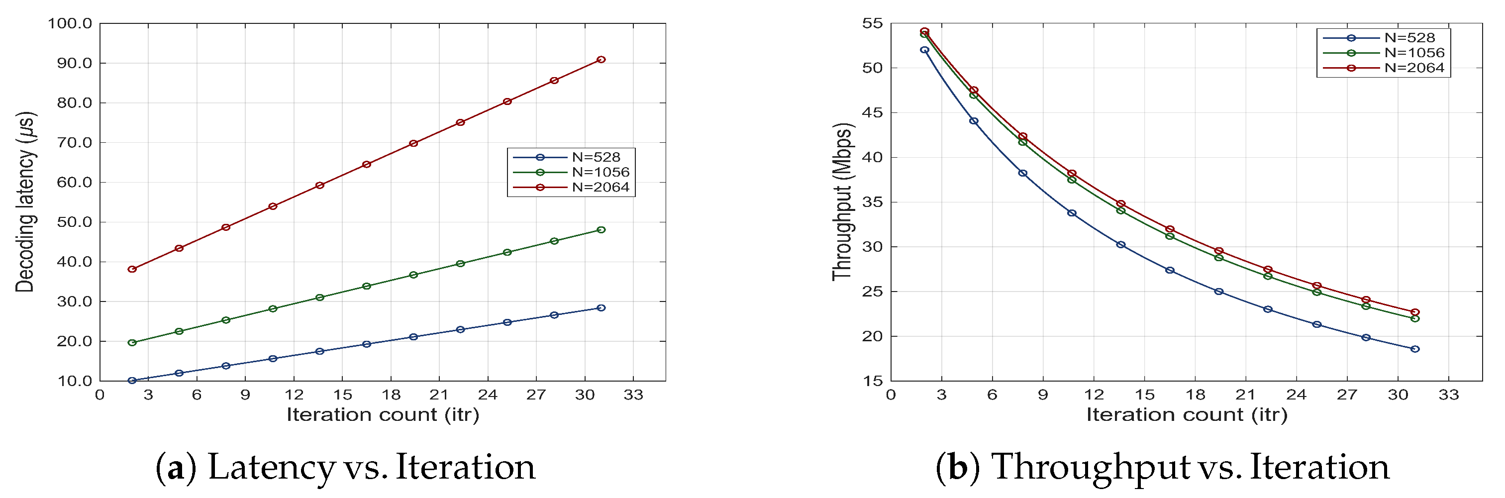
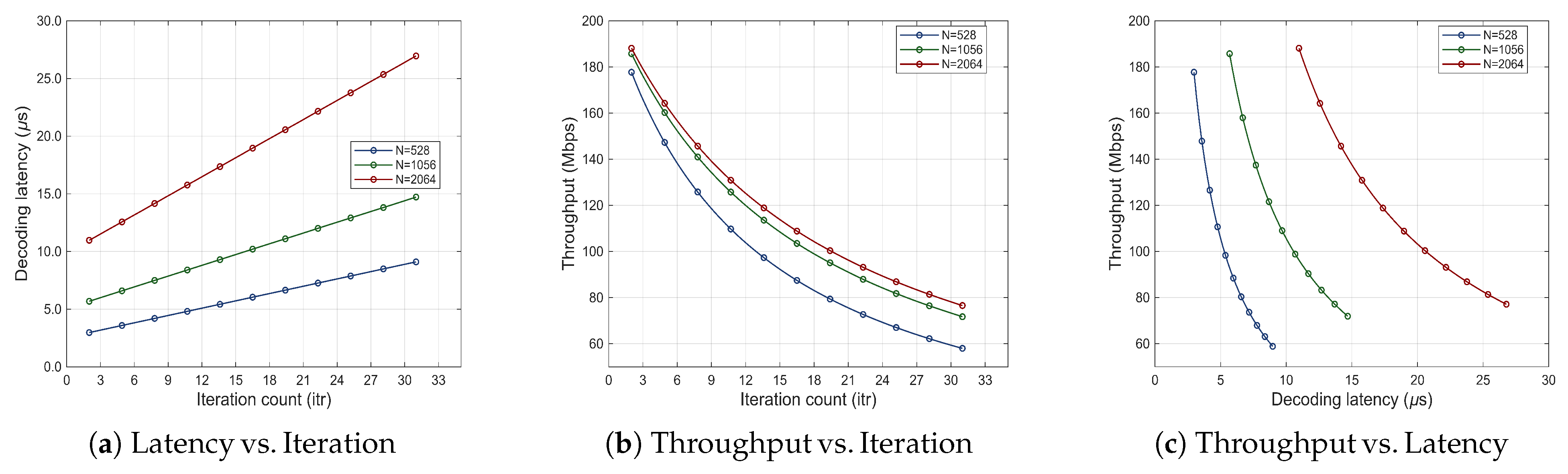
As summarized in Figure 9, the decoding latency as a function of the iteration limit for N { 528 , 1056 , 2064 } is illustrated in Figure 9a, whereas Figure 9b reports the corresponding throughput trend at F clk = 100 MHz . The latency curves grow almost linearly with the number of iterations, which indicates that each additional iteration contributes an approximately constant extra delay. For larger block lengths, the slope is steeper, reflecting the increased amount of message-processing work per iteration.
In contrast, the throughput curves decrease monotonically with the iteration budget because longer processing time per codeword directly reduces the number of codewords that can be decoded per second. For any fixed iteration limit, the larger block sizes achieve slightly higher throughput since the fixed I/O and control overheads are amortized over more decoded bits. The same qualitative behavior is observed at F clk = 350 MHz reported in Appendix D.
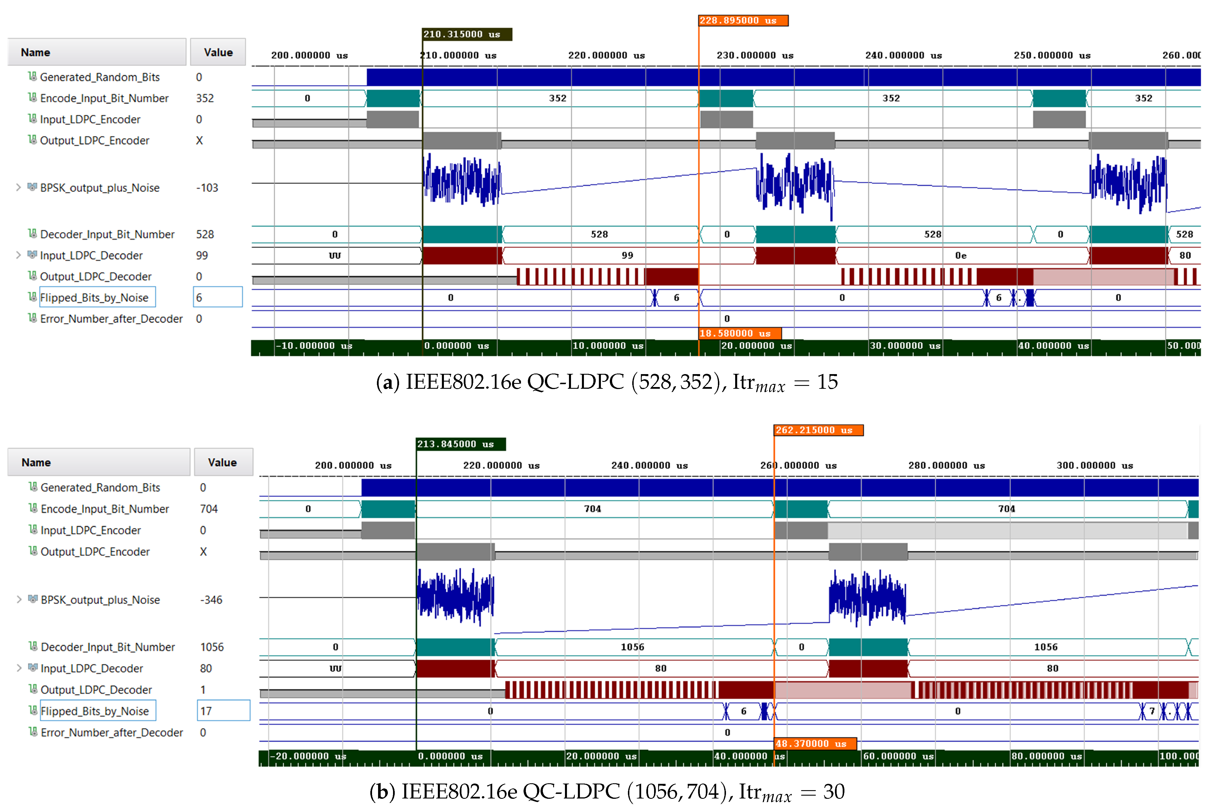
To experimentally validate the 2D-CNMS decoder latency model in (14) and corroborate the post-synthesis estimates in Table 4, Figure 10 presents representative RTL simulation traces obtained in Xilinx Vivado 2024 for the ( 528 , 352 ) and ( 1056 , 704 ) QC-LDPC codes. For each configuration, the left cursor is aligned with the first valid AXI4-Stream LLR sample at the decoder input, and the right cursor marks the last valid hard-decision bit at the decoder output. Between these two cursors, the cyan input counters ramp over N samples, after which the decoder enters its iterative processing phase, clearly visible as the dark-red activity region in the decoder waveforms. For the ( 528 , 352 ) code (Figure 10a), the decoder is configured with Itr max = 15 , producing 15 almost identical dark-red segments and a total measured latency of approximately 18.6 μ s . For the ( 1056 , 704 ) code (Figure 10b), Itr max = 32 iterations are enabled, resulting in a longer dark-red region and a latency of about 48.4 μ s . We deliberately choose different iteration limits for the two block lengths to make the impact of the iteration budget on the overall latency visually evident: each additional iteration extends the dark-red decoder activity by approximately a constant amount, which is consistent with the iteration-dependent term in the latency model of (14) and with the nearly linear latency-iteration relationship observed in Figure 9a.

8. Conclusions

This work presented an end-to-end FPGA implementation of a QC-LDPC decoder for VSATPlus systems using Vitis HLS 2025 and Vivado 2024. The primary contribution lies in demonstrating a practical design methodology for mapping advanced LDPC decoding techniques onto FPGA hardware through HLS-driven flows, enabling rapid prototyping and deployment without manual RTL development. The proposed architecture employs shift-and-subtract operations to eliminate multipliers and dividers, resulting in a DSP-free design optimized for resource-constrained satellite terminals. The complete system integration was achieved using HLS-generated IP cores for the encoder, AWGN channel, and decoder. Under a 100 MHz clock, the decoder attains a coded-bit throughput of 29–41 Mbps with optimized resource utilization, while maintaining low implementation complexity. Fixed scaling factors were selected through empirical optimization to balance BER performance and hardware simplicity, avoiding the complexity overhead of adaptive scaling with negligible performance penalty. Performance evaluation under AWGN, which is appropriate for geostationary Earth orbit (GEO) VSATPlus links with negligible Doppler and stable fading, shows near-SP decoding performance and no observable error floor down to BER < 10 8 . Compared with MS-family baselines, the implemented design achieves faster convergence and lower iteration counts, translating into reduced latency and higher throughput.
Future work will extend this HLS-based methodology beyond AWGN baselines by assessing robustness under non-Gaussian and interference-rich satellite communications (SATCOM) conditions (e.g., narrowband and partial-band interference, pulsed and swept jamming, adjacent-channel interference, and time-varying intelligent jamming). In this context, we will also consider lightweight cross-layer hooks between FEC and higher-layer counter-jamming mechanisms, where deep reinforcement learning (DRL)-based strategies are one possible option, for example, by exploiting decoder reliability indicators to enable adaptive operation, as motivated by dual-intelligence satellite/terminal counter-jamming frameworks [52]. In parallel, we will further connect this work with CNN-based LDPC decoding by targeting “colored’’ noise (e.g., 1/f-type correlation) to adapt decoding and scheduling for improved end-to-end throughput and resilience [23].

Author Contributions

Conceptualization, N.K.; methodology, N.K.; software, N.K.; formal analysis, N.K.; investigation, N.K.; writing—original draft preparation, N.K.; visualization, N.K. and R.M.; writing—review and editing, R.M. and M.R.S.; supervision, M.R.S.; project administration, R.M.; funding acquisition, none. All authors have read and agreed to the published version of the manuscript.

Funding

This research received no external funding.

Data Availability Statement

The datasets presented in this article are not publicly available due to commercial and confidentiality restrictions.

Conflicts of Interest

Author Ron Mankarious was employed by the company PolarSat Inc. The remaining authors declare that the re-search was con-ducted in the absence of any commercial or financial relationships that could be construed as a potential conflict of interest.

Appendix A

The material collected in this appendix documents the supporting blocks and test setup used to evaluate the proposed layered 2D-CNMS LDPC decoder on FPGA. In particular, we describe the QC-LDPC encoder and the AWGN channel generation chain, implemented in Vitis HLS 2025 and deployed in Vivado 2024, which together form the end-to-end FEC path required for validating the decoder in a realistic modem environment. These components are based on well-established standards and algorithms and are therefore not part of the core algorithmic contribution; however, their hardware realization is essential for reproducibility and for demonstrating that the complete encoder-channel-decoder chain can be implemented consistently within the same HLS-to-FPGA flow. To keep the main body of the paper focused on the novel decoder architecture, its hardware-aware optimization, and comparative performance, the detailed description of these auxiliary blocks is provided in Appendix B and Appendix C.

Appendix B. QC-LDPC Encoder

The QC-LDPC encoder implemented in this work is based on the IEEE C 802.16 e standard [30], which introduces a harmonized definition of QC-LDPC codes for the orthogonal frequency-division multiple access (OFDMA) physical layer, developed collaboratively by six major industry contributors including Intel, Motorola, Nokia, Nortel, Samsung, and Texas Instruments. The proposed LDPC codes are based on structured base matrices expanded into large parity-check matrices using circulant permutation matrices. This method utilizes a recursive structure with circular shifts and XOR operations facilitating streamlined hardware implementation and efficient computational logic on FPGA platforms. The standard supports multiple code rates (1/2, 2/3, and 3/4) and a wide range of block sizes through scalable expansion, shortening, and puncturing techniques, making it well suited for modern, high-throughput communication systems of a VSATPlus satellite communications system.

Appendix B.1. VSATPlus Encoder Algorithm
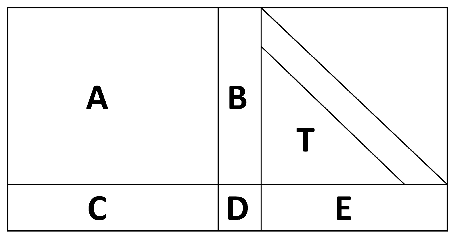
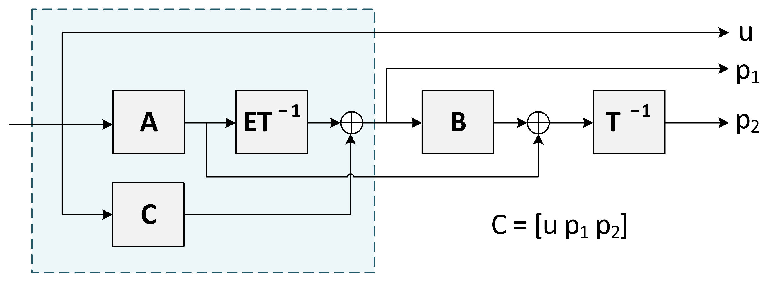
The VSATPlus QC-LDPC encoder leverages the Direct Encoding Method II as specified in the IEEE C802.16e-04/373r1 standard [30]. This approach is grounded in a structured matrix-partitioning technique that facilitates deterministic, low-complexity encoding suitable for hardware implementation. As illustrated in Figure A1, the parity-check matrix H is decomposed into six sub-matrices: A ( N p g ) × N k , B ( N p g ) × g , C g × N k , D g × g , E g × ( N p g ) , and T ( N p g ) × ( N p g ) , with T being a lower-triangular matrix characterized by ones along its main diagonal.
Figure A1. Structure of the QC-LDPC parity-check matrix implemented for VSATPlus based on IEEE 802.16 e [30].
Aerospace 13 00155 g0a1
In the QC-LDPC selected for implementation and evaluation in this work, the instantiated parameters ( N p , N k , g ) are ( 12 , 12 , 1 ) , ( 8 , 16 , 1 ) , and ( 12 , 36 , 1 ) for R = 1 / 2 , 2 / 3 , 3 / 4 , respectively, where N p and N k denote the permutation-matrix rows and columns with lifting factor Z = N / ( N k + N p ) . The instantiate block lengths in our experiments are { 528 , 1056 , 2064 } with the three code rates.
Given a systematic input vector u, the encoding procedure begins with the computation of intermediate products A u T and C u T , followed by the application of the inverse transform T 1 ( A u T ) . The first set of parity bits, denoted p 1 , is then computed according to
p 1 T = C u T + E T T 1 ( A u T ) ,
which incorporates contributions from both the C and E matrices. Subsequently, the second set of parity bits, p 2 , is obtained using
p 2 T = T 1 ( A u T + B p 1 T ) ,
where the input u and partial parity p 1 are jointly encoded via the lower-triangular transformation. A high-level depiction of this block-wise encoding flow is provided in Figure A2.
Figure A2. Block diagram of the IEEE 802.16 e QC-LDPC encoder architecture [30].
Aerospace 13 00155 g0a2
The matrix sparsity and hierarchical decomposition yield a high-throughput, pipelined encoder design with minimal logic complexity. For a detailed derivation and theoretical justification of (A1) and (A2), refer to [30].

Appendix B.2. FPGA Implementation of VSATPlus Encoder

The QC-LDPC encoder is implemented using Vitis HLS 2025 and synthesized for the XilinxZynq UltraScale+ MPSoC (AMD Xilinx, San Jose, CA, USA) device with a target system clock of 100 MHz. The implementation leverages extensive high-level synthesis optimizations including loop pipelining, aggressive unrolling, and complete array partitioning. These transformations enable deep parallelism across matrix-vector computations and circular shift operations, particularly within encoding stages. A detailed summary of the post-RTL optimized resource utilization, latency, and throughput for the specific QC-LDPC codes is presented in Table A1.
Table A1. QC-LDPC encoder resource utilization.
Resource R = 2 / 3 Avail.
(528,352)(1056,704)(2064,1376)
LUT 112820323668 117,120
FF 107919403570 234,240
DSP 2221248
BRAM -18 K000288
URAM  100064
SRL 586166
LATCH 000
CLB 000
SLICE 000
Latency 91117923473
Γ (Mbps)585960
1 UltraRAM: 64-blocks, 288 Kb each. 2 Latency: in clock cycles at @ 100 MHz .
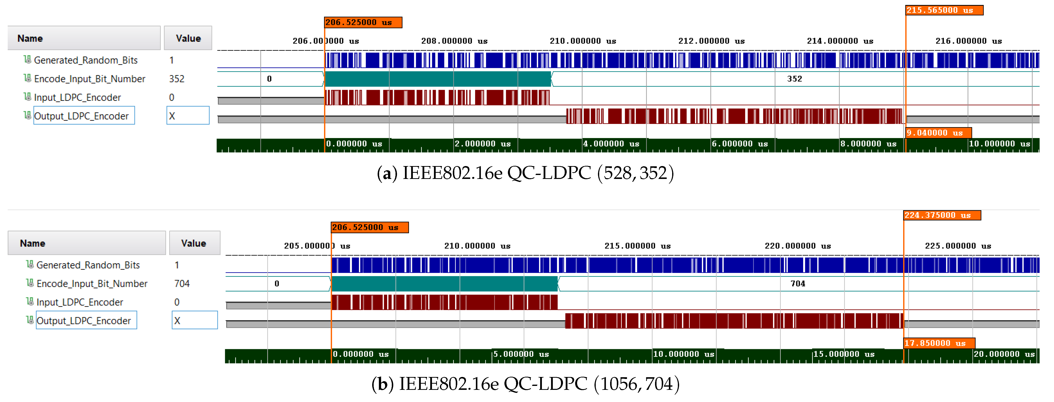
Figure A3 illustrates RTL simulation traces of the QC-LDPC encoder at F c l k = 100 MHz in Vivado 2024. In each case, the left cursor is aligned with the first valid AXI4-Stream input word and the right cursor with the last valid encoded bit at the output port. The internal counters ramp over the K accepted information bits and the N emitted code bits, confirming correct framing for the ( 528 , 352 ) and ( 1056 , 704 ) configurations. The output interface operates without backpressure, and only a small pipeline fill/drain overhead is visible in the ready/valid handshakes. For the ( 528 , 352 ) and ( 1056 , 704 ) codes, the cursor span corresponds to 904 and 1787 cycles, respectively, at 100 MHz, in close agreement with the Vitis HLS 2025 latency reported in Table A1.
Figure A3. Encoder latency analysis of QC-LDPC with F c l k = 100 MHz via Xilinx Vivado 2024.
Aerospace 13 00155 g0a3

Appendix C. FPGA Implementation of an AWGN Channel

To evaluate QC-LDPC code in communication link, a dedicated AWGN noise generator is synthesized using Vitis HLS 2025 and integrated into the FPGA design via IP instantiation in Xilinx Vivado Design Suite 2024. The generator is clocked at 100 MHz and implements the Box–Muller transformation using fixed-point arithmetic and LUT-based approximations [53]. The Box–Muller method converts two statistically independent and identically distributed (i.i.d.) random variables U 1 , U 2 ( 0 , 1 ) into a pair of independent, standard normally distributed variables, as follows:
N I = 2 ln U 1 × cos ( 2 π U 2 )
N Q = 2 ln U 1 × sin ( 2 π U 2 )
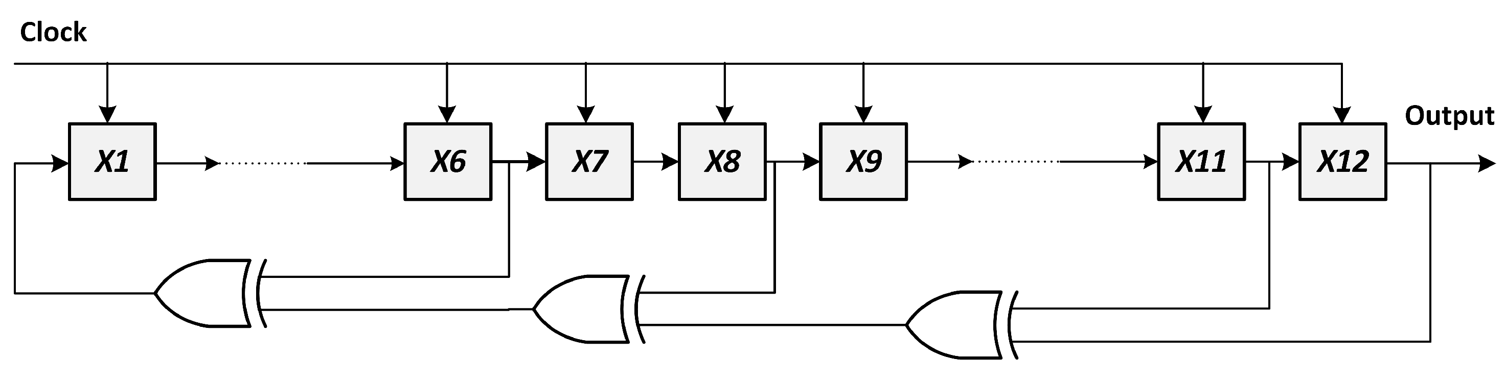
where N I , N Q N ( 0 , 1 ) . The FPGA-based AWGN generator is architected for cycle-accurate, pipelined synthesis of zero-mean Gaussian noise samples. To minimize hardware complexity and maximize throughput, computationally intensive functions, such as logarithmic operation, are replaced with high-resolution fixed-point LUTs generated offline using Python 3.10.12, which map i.i.d. random variables to radius values R = 2 ln U 1 , and cos ( 2 π U 2 ) . Address generation for the LUTs is driven by two decorrelated 12-bit LFSRs, seeded independently and defined by the primitive polynomial of g ( X ) = X 12 + X 11 + X 8 + X 6 , as illustrated in Figure A4.
Figure A4. 12-bit LFSR with 1-bit output used in the Box–Muller method to generate i.i.d. random variable.
Aerospace 13 00155 g0a4
This primitive polynomial ensures maximal-length pseudo-random sequences. Each LFSR output is truncated to 10 bits, enabling indexed access to LUTs of size 1024, corresponding to a 10-bit address space. To maintain statistical zero-mean behavior, a DC offset correction stage is implemented using a programmable exponential moving average (EMA) applied to the noise sample. The DC bias estimate, b [ n ] , is iteratively updated, and the DC-corrected output is then computed as follows:
N centered [ n ] = N [ n ] b [ n + 1 ]
b [ n + 1 ] = b [ n ] + 1 2 ζ N [ n ] b [ n ]
where ζ is a configurable smoothing coefficient. The bias-corrected sample is subsequently saturated to the 14-bit signed output range [ 8192 , + 8191 ] . The entire architecture is fully pipelined, delivering one valid output sample per clock cycle.
On Xilinx Zynq UltraScale+ MPSoC (AMD Xilinx, San Jose, CA, USA) devices, the ARM-based PS provides the control plane for the AWGN IP, exposing all configuration knobs through an AXI4-Lite register file while the I/Q samples stream over AXI4-Stream. In our design, the PS programs noise standard deviation, EMA shift controlling the bias-removal time constant, ζ in (A6), and the independent seeds that decorrelate the two LFSR-driven LUT address generators.
Table A2 summarizes post-synthesis resource usage for the AWGN IP-core, comparing HLS estimates with Vivado 2024 results. Overall utilization on the target device is very low, with single-digit DSP and BRAM usage, no URAM.
Table A2. AWGN IP-core design resource utilization.
ResourceHLSVivadoAvail.
UsedUtil. (%)UsedUtil. (%)
LUT1545 1.30 43253.68 117,120
FF515 0.21 27441.16 234,240
DSP8 0.64 40.321248
BRAM-18K3 1.04 10.35288
URAM0-0- 64   1
SRL0-66--
LATCH0-0--
CLB0-0--
1 UltraRAM: 64-blocks, 288 Kb each.

Appendix D. Supplementary Latency and Throughput Results

For completeness, Figure A5 reports the latency and throughput behavior of the implemented decoder at F clk = 350 MHz for block lengths N { 528 , 1056 , 2064 } . Figure A5a shows the decoding latency as a function of the iteration limit, while Figure A5b presents the corresponding throughput trend. Increasing the clock frequency significantly improves the sustained throughput while preserving the qualitative throughput–latency trade-off observed at 100 MHz (see Figure 9): latency grows almost linearly with the iteration budget, and throughput decreases accordingly because of the longer per-codeword processing time. For a fixed iteration limit, larger block lengths achieve slightly higher throughput, since the fixed control and I/O overheads are amortized over more decoded bits. Figure A5 summarizes these results as an explicit throughput–latency trade-off at 350 MHz .
Figure A5. 2D-CNMS decoder latency and throughput trends for different block lengths at R = 1 / 2 @ 350 MHz : (a) latency versus iteration; (b) throughput versus iteration; (c) throughput versus latency.
Aerospace 13 00155 g0a5

References

  1. Cross, M.A.; Fleetwood, T. Hubless VSAT networks. In IEE Colloquium on VSATs—Trends and Technologies; IEEE: Piscataway, NJ, USA, 1989; pp. 5/1–5/13. [Google Scholar]
  2. ETSI TS 136 201 V15.2.0; Evolved Universal Terrestrial Radio Access (E-UTRA); LTE Physical Layer—General Description. ETSI: Valbonne, France, 2017.
  3. ETSI EN 302 307 V1.4.1; Digital Video Broadcasting (DVB); Second Generation Framing Structure, Channel Coding and Modulation Systems for Broadcasting, Interactive Services, News Gathering and Other Broadband Satellite Applications (DVB-S2). ETSI: Valbonne, France, 2009.
  4. ETSI EN 300 744 V1.6.1; Digital Video Broadcasting (DVB); Framing Structure, Channel Coding and Modulation for Digital Terrestrial Television (DVB-T). ETSI: Valbonne, France, 2009.
  5. ETSI ES 300 401 V1.4.1; Radio Broadcast Systems; Digital Audio Broadcasting (DAB) to Mobile, Portable and Fixed Receivers. ETSI: Valbonne, France, 1995.
  6. ETSI GSM 05.05; Digital Cellular Telecommunications System (Phase 2+); Radio Transmission and Reception (GSM). ETSI: Valbonne, France, 1996.
  7. ETSI EN 302 769 V1.3.1; Digital Video Broadcasting (DVB); Frame Structure, Channel Coding and Modulation for a Second Generation Digital Transmission System for Cable Systems (DVB-C2). ETSI: Valbonne, France, 2009.
  8. Khosroshahi, N.; Gulliver, T.A. Quasi-cyclic low density parity check (LDPC) codes for dedicated short range communication (DSRC) systems. In CCECE 2010; IEEE: Piscataway, NJ, USA, 2010; pp. 1–5. [Google Scholar] [CrossRef]
  9. 802.11-2020; IEEE Standard for Local and Metropolitan Area Networks—Specific Requirements—Part 11: Wireless LAN Medium Access Control (MAC) and Physical Layer (PHY) Specifications. IEEE: Piscataway, NJ, USA, 2009.
  10. 3GPP TS 38.212 V15.2.0; 3rd Generation Partnership Project; Technical Specification; 5G; NR; Multiplexing and Channel Coding. ETSI: Valbonne, France, 2018.
  11. Chung, K.; Cho, K.; Lee, W.-H. Simplified 2-dimensional scaled min-sum algorithm for LDPC decoder. J. Electr. Eng. Technol. 2017, 12, 1262–1270. [Google Scholar] [CrossRef]
  12. MacKay, D.J.C. Good error-correcting codes based on very sparse matrices. IEEE Trans. Inf. Theory 1999, 45, 399–431. [Google Scholar] [CrossRef]
  13. Fossorier, M.P.C.; Mihaljevic, M.; Imai, H. Reduced complexity iterative decoding of low-density parity check codes based on belief propagation. IEEE Trans. Commun. 1999, 47, 673–680. [Google Scholar] [CrossRef]
  14. Wiberg, N.; Loeliger, H.-A.; Kotter, R. Codes and iterative decoding on general graphs. In Proceedings of the 1995 IEEE International Symposium on Information Theory, Whistler, BC, Canada, 17–22 September 1995; IEEE: Piscataway, NJ, USA, 1995; p. 468. [Google Scholar] [CrossRef]
  15. Lopez, H.; Chan, H.-W.; Chiu, K.-L.; Tsai, P.-Y.; Jou, S.-J.J. A 75-Gb/s/mm2 and energy-efficient LDPC decoder based on a reduced complexity second minimum approximation min-sum algorithm. IEEE Trans. Very Large Scale Integr. (VLSI) Syst. 2020, 28, 926–939. [Google Scholar] [CrossRef]
  16. Hamad, A. Estimation of two-dimensional correction factors for min-sum decoding of regular LDPC code. Wirel. Eng. Technol. 2013, 4, 181–187. [Google Scholar] [CrossRef][Green Version]
  17. Boncalo, O.; Amaricai, A. Ultra high throughput unrolled layered architecture for QC-LDPC decoders. In Proceedings of the 2017 IEEE Computer Society Annual Symposium on VLSI (ISVLSI), Bochum, Germany, 3–5 July 2017; IEEE: Piscataway, NJ, USA, 2017; pp. 225–230. [Google Scholar] [CrossRef]
  18. Yang, N.; Jing, S.; Yu, A.; Liang, X.; Zhang, Z.; You, X.; Zhang, C. Reconfigurable decoder for LDPC and polar codes. In Proceedings of the 2018 IEEE International Symposium on Circuits and Systems (ISCAS), Florence, Italy, 27–30 May 2018; IEEE: Piscataway, NJ, USA, 2018; pp. 1–5. [Google Scholar] [CrossRef]
  19. Bhatt, T.; Sundaramurthy, V.; Stolpman, V.; McCain, D. Pipelined block-serial decoder architecture for structured LDPC codes. In Proceedings of the 2006 IEEE International Conference on Acoustics Speech and Signal Processing Proceedings, Toulouse, France, 14–19 May 2006; IEEE: Piscataway, NJ, USA, 2006; Volume 4, p. IV. [Google Scholar] [CrossRef]
  20. Mansour, M.M. A turbo-decoding message-passing algorithm for sparse parity-check matrix codes. IEEE Trans. Signal Process. 2006, 54, 4376–4392. [Google Scholar] [CrossRef]
  21. Richardson, T.J.; Urbanke, R.L. The capacity of low-density parity-check codes under message-passing decoding. IEEE Trans. Inf. Theory 2001, 47, 599–618. [Google Scholar] [CrossRef]
  22. PolarSat Inc. VSATPlus3® Overview. 2003. Available online: https://www.polarsat.com/vsatplus-3 (accessed on 1 January 2026).
  23. Khosroshahi, N.; Mankarious, R.; Soleymani, M.R. CNN-Based LDPC Decoder for Hubless Full-Mesh VSATPlus® System. In Proceedings of the 2025 AIAA DATC/IEEE 44th Digital Avionics Systems Conference (DASC), Montreal, QC, Canada, 14–18 September 2025; IEEE: Piscataway, NJ, USA, 2025; pp. 1–8. [Google Scholar] [CrossRef]
  24. Fossorier, M.P.C. Quasicyclic low-density parity-check codes from circulant permutation matrices. IEEE Trans. Inf. Theory 2004, 50, 1788–1793. [Google Scholar] [CrossRef]
  25. Gal, B.L.; Jego, C.; Leroux, C. A flexible NISC-based LDPC decoder. IEEE Trans. Signal Process. 2014, 62, 2469–2479. [Google Scholar] [CrossRef]
  26. Tamkeen, S.A.; Hamad, A.A. FPGA implementation of scaled “Quasi-Cyclic LDPC” decoder using high-level synthesis. In Proceedings of First International Conference on Mathematical Modeling and Computational Science: ICMMCS 2020; Springer: Singapore, 2021; pp. 131–142. [Google Scholar] [CrossRef]
  27. Wiberg, N. Codes and Decoding on General Graphs. Ph.D. Dissertation, Department of Electrical Engineering, Linköping University, Linköping, Sweden, 1996. [Google Scholar]
  28. Tanner, R.M. A recursive approach to low complexity codes. IEEE Trans. Inf. Theory 1981, 27, 533–547. [Google Scholar] [CrossRef]
  29. 802.16-2009; IEEE Standard for Local and Metropolitan Area Networks—Part 16: Air Interface for Broadband Wireless Access Systems. IEEE: Piscataway, NJ, USA, 2009.
  30. IEEE 802.16 Working Group LDPC Coding for OFDMA PHY Contribution to IEEE 802.16e. 2004. Available online: http://ieee802.org/16/tge/contrib/C80216e-04_373r1.pdf (accessed on 1 January 2026).
  31. Wang, Q.; Liu, Q.; Wang, S.; Chen, L.; Fang, H.; Chen, L.; Guo, Y.; Wu, Z. Normalized min-sum neural network for LDPC decoding. IEEE Trans. Cogn. Commun. Netw. 2023, 9, 70–81. [Google Scholar] [CrossRef]
  32. Oh, D.; Parhi, K.K. Min-sum decoder architectures with reduced word length for LDPC codes. IEEE Trans. Circuits Syst. I Regul. Pap. 2010, 57, 105–115. [Google Scholar] [CrossRef]
  33. Zhong, Z.; Guo, S.; Xu, X.; Bai, H. A classified normalized BP-based algorithm with 2-dimensional correction for LDPC codes. J. Commun. 2013, 8, 315–321. [Google Scholar] [CrossRef][Green Version]
  34. Martin, G.; Smith, G. High-Level Synthesis: Past, Present, and Future. IEEE Des. Test Comput. 2009, 26, 18–25. [Google Scholar] [CrossRef]
  35. AMD Xilinx. Vivado Design Suite User Guide: High-Level Synthesis UG902 V2020.1. 2021. Available online: https://docs.amd.com/v/u/en-US/ug902-vivado-high-level-synthesis (accessed on 1 January 2026).
  36. Delomier, Y.; Gal, B.L.; Crenne, J.; Jego, C. Model-based design of flexible and efficient LDPC decoders on FPGA devices. J. Signal Process. Syst. 2020, 92, 727–745. [Google Scholar] [CrossRef]
  37. Li, J.; Zhang, P.; Wang, L.; Wang, G. An FPGA-Based LDPC Decoder with Optimized Scale Factor in NMS Decoding Algorithm. J. Meas. Sci. Instrum. 2022, 13, 398–406. [Google Scholar] [CrossRef]
  38. Wey, C.-L.; Shieh, M.-D.; Lin, S.-Y. Algorithms of finding the first two minimum values and their hardware implementation. IEEE Trans. Circuits Syst. I Regul. Pap. 2008, 55, 3430–3437. [Google Scholar] [CrossRef]
  39. Tanyanon, I.; Choomchuay, S. A hardware design of MS/MMS-based LDPC decoder. In Proceedings of the 2012 IEEE International Conference on Electron Devices and Solid State Circuit (EDSSC), Bangkok, Thailand, 3–5 December 2012; IEEE: Piscataway, NJ, USA, 2012; pp. 1–4. [Google Scholar] [CrossRef]
  40. Andrade, J.; Falcão, G.; Silva, V. Flexible design of wide-pipeline-based WiMAX QC-LDPC decoder architectures on FPGAs using high-level synthesis. IET Electron. Lett. 2014, 50, 839–840. [Google Scholar] [CrossRef]
  41. Scheiber, E.; Bruck, G.H.; Jung, P. Implementation of an LDPC decoder for IEEE 802.11n using Vivado™ High-Level Synthesis. WSEAS Trans. Acoust. Music. 2013, 8, 1–4. [Google Scholar] [CrossRef]
  42. Andrade, J.; Pratas, F.; Falcao, G.; Silva, V.; Sousa, L. Combining flexibility with low power: Dataflow and wide-pipeline LDPC decoding engines in the Gbit/s era. In Proceedings of the 2014 IEEE 25th International Conference on Application-Specific Systems, Architectures and Processors, Zurich, Switzerland, 18–20 June 2014; IEEE: Piscataway, NJ, USA, 2014; pp. 264–269. [Google Scholar] [CrossRef]
  43. Zied, S.A.; Sayed, A.T.; Guindi, R. Configurable low complexity decoder architecture for Quasi-Cyclic LDPC codes. In Proceedings of the 2013 21st International Conference on Software, Telecommunications and Computer Networks—(SoftCOM 2013), Split, Croatia, 18–20 September 2013; IEEE: Piscataway, NJ, USA, 2013; pp. 1–5. [Google Scholar] [CrossRef]
  44. Zhao, W.H.; Long, J.P. Implementing the NASA Deep Space LDPC Codes for Defense Applications. In Proceedings of the MILCOM 2013—2013 IEEE Military Communications Conference, San Diego, CA, USA, 18–20 November 2013; IEEE: Piscataway, NJ, USA, 2013; pp. 803–808. [Google Scholar] [CrossRef]
  45. Gal, B.L.; Jego, C. Design of an ASIP LDPC Decoder Compliant with Digital Communication Standards. In Proceedings of the 2012 IEEE Workshop on Signal Processing Systems, Quebec City, QC, Canada, 17–19 October 2012; IEEE: Piscataway, NJ, USA, 2012; pp. 19–24. [Google Scholar] [CrossRef]
  46. Mhaske, S.; Kee, H.; Ly, T.; Aziz, A.; Spasojevic, P. FPGA-Based Channel Coding Architectures for 5G Wireless Using High-Level Synthesis. Int. J. Reconfigurable Comput. 2017, 2017, 3689308. [Google Scholar] [CrossRef]
  47. Mhaske, S.; Kee, H.; Ly, T.; Aziz, A.; Spasojevic, P. High-Throughput FPGA-Based QC-LDPC Decoder Architecture. In Proceedings of the 2015 IEEE 82nd Vehicular Technology Conference (VTC2015-Fall), Boston, MA, USA, 6–9 September 2015; IEEE: Piscataway, NJ, USA, 2015; pp. 1–5. [Google Scholar] [CrossRef]
  48. Amaricai, A.; Boncalo, O.; Mot, I. Memory efficient FPGA implementation for flooded LDPC decoder. In Proceedings of the 2015 23rd Telecommunications Forum Telfor (TELFOR), Belgrade, Serbia, 24–26 November 2015; IEEE: Piscataway, NJ, USA, 2015; pp. 500–503. [Google Scholar] [CrossRef]
  49. Pignoly, V.; Gal, B.L.; Jego, C.; Gadat, B. High data rate and flexible hardware QC-LDPC decoder for satellite optical communications. In Proceedings of the 2018 IEEE 10th International Symposium on Turbo Codes & Iterative Information Processing (ISTC), Hong Kong, China, 3–7 December 2018; IEEE: Piscataway, NJ, USA, 2018; pp. 1–5. [Google Scholar] [CrossRef]
  50. Zhang, Y.; Cao, Q.; Wang, S.; Yao, J.; Jiang, H. HF-LDPC: HLS-friendly QC-LDPC FPGA decoder with high throughput and flexibility. In Proceedings of the 2023 IEEE 41st International Conference on Computer Design (ICCD), Washington, DC, USA, 6–8 November 2023; IEEE: Piscataway, NJ, USA, 2023; pp. 566–573. [Google Scholar] [CrossRef]
  51. Zhang, Y.; Cao, Q.; Yao, J.; Jiang, H. R-LDPC: Refining behavior descriptions in HLS to implement high-throughput LDPC decoder. In Proceedings of the 2023 Design, Automation & Test in Europe Conference & Exhibition (DATE), Antwerp, Belgium, 17–19 April 2023; IEEE: Piscataway, NJ, USA, 2023; pp. 1–6. [Google Scholar] [CrossRef]
  52. Wang, H.; Ouyang, Q.; Xi, W.; Xiang, Y.; Ye, N. Dual Intelligence: Leveraging DRL with Smart Satellites to Counter Intelligent Jamming in Satellite Networks. IEEE Trans. Cogn. Commun. Netw. 2026, 12, 1054–1067. [Google Scholar] [CrossRef]
  53. Çağlan, A.; İnceöz, E.; Balcısöy, E.; Özbek, M.; Çavuş, E. FPGA implementation of AWGN noise generator using Box–Muller method. In Proceedings of the 2016 24th Signal Processing and Communication Application Conference (SIU), Zonguldak, Turkey, 16–19 May 2016; IEEE: Piscataway, NJ, USA, 2016; pp. 1813–1816. [Google Scholar] [CrossRef]
Figure 1. Example: VSATPlus full-mesh, hubless deployment for ATC applications.
Aerospace 13 00155 g001
Figure 2. VSATPlus full-mesh, hubless network architecture for satellite communication.
Aerospace 13 00155 g002
Figure 3. Sparsity pattern of the parity-check matrix H for QC-LDPC ( N = 1056 , K = 704 ) [30].
Aerospace 13 00155 g003
Figure 4. FPGA-based architecture of 2D-CNMS decoder.
Aerospace 13 00155 g004
Figure 5. Vivado 2024 end-to-end block design integrating HLS-generated IP cores.
Aerospace 13 00155 g005
Figure 6. Performance comparison for QC-LDPC ( 1056 , 704 ) with Itr max = 50 .
Aerospace 13 00155 g006
Figure 7. BER performance versus SNR and iteration count: (a,b) NMS and (c,d) 2D-CNMS.
Aerospace 13 00155 g007
Figure 8. Performance analysis of QC-LDPC codes under 2D-CNMS decoding algorithm.
Aerospace 13 00155 g008
Figure 9. 2D-CNMS decoder latency and throughput trends for different block lengths at R = 1 / 2 @ 100 MHz : (a) latency versus iteration; (b) throughput versus iteration.
Aerospace 13 00155 g009
Figure 10. 2D-CNMS decoder latency analysis of QC-LDPC instances with F c l k = 100 MHz via Xilinx Vivado 2024: (a) IEEE 802.16 e QC-LDPC ( 528 , 352 ) with Itr max = 15 ; (b) IEEE 802.16 e QC-LDPC ( 1056 , 704 ) with Itr max = 30 .
Aerospace 13 00155 g010
Table 2. Computational complexity of a check node within a single iteration.
Ref.AlgorithmMult.Div.ComparisonAdd.Sub.Bit-ShiftFPGA Impl.Remarks
[12]SP d c d c 1 0100tanh, tanh 1
[38]MS00 d c + log 2 d c 2 000
[31]NMS10 d c + log 2 d c 2 000
[32]OMS00 d c + log 2 d c 2 010
[39] N M S 00 d c + log 2 d c 2 4012 β = 0.75
[16]2D-MS20 d c + log 2 d c + 2 000adaptive
[26]2D-MS20 d c + log 2 d c 2 000 α ¯ = β ¯ = 0.899
[33]2D-NMS20 d c + log 2 d c 2 000
[32]2D-NMS20 d c + log 2 d c 2 000 β 1 = 0.75 , β 2 = 0.875
α ¯ = 0.75
Ourwork2D-CNMS00 d c + log 2 d c 2 0312 β 1 ¯ = 0.8125
β 2 ¯ = 0.875
Table 3. Previous LDPC decoder implementations on various FPGA platforms.
MethodTypeDecoderScheduleStandardNRateItr. f clk (MHz) Γ (Mbps)Logic 1RAM 2
[40] HLS MS Flooding 802.16 e 768 1 / 2 10 211.1 99 147,000 1641
[40] HLS MS Flooding 802.16 e 1152 1 / 2 10 222.6 104 161,000 1703
[40] HLS MS Flooding 802.16 e 1536 1 / 2 10 203.5 82 134,000 1461
[40] HLS MS Flooding 802.16 e 1920 1 / 2 10 202.4 81 144,000 1516
[41] HLS MS Flooding 802.11 n 648 1 / 2 312227907228
[42] FPGA MS Layered 802.11 n 1944 1 / 2 1015721 187,000 1349
[43] FPGA MS Layered 802.11 n 648 1 / 2 6100281 35,668 81
[44] FPGA MS Layered custom1024 1 / 2 30175- 25,035 72
[45] FPGA OMS Layered 802.16 e 576 1 / 2 20100338685106
[45] FPGA OMS Layered 802.16 e 2304 1 / 2 10100307 34,104 281
[46] FPGA MS Layered 802.11 n 972 1 / 2 42002476 159,000 831
[46] FPGA OMS Layered 802.11 n 1944 1 / 2 4200608 33,351 120
[47] FPGA OMS Layered 802.11 n 1944 1 / 2 8260608 33,351 102
[48] FPGA MS Flooding 802.16 e 2304 1 / 2 20260290<15,52076
[39] FPGA OMS Layered 802.11 n 648 1 / 2 519477 19,332 3
[49] FPGA OMS Layered DVB - S 2 16 , 384 1 / 2 102502130 49,121 50
[50] FPGA MS Layered 802.16 e 1536 1 / 2 5-209 14,000 -
[51] FPGA MS Layered 802.16 e 1152 1 / 2 10330188 25,621 76
FPGA 2D-CNMS Layered 802.16 e 528 1 / 2 151002996960
Our-work FPGA 2D-CNMS Layered 802.16 e 1056 1 / 2 1510034 10,343 0
FPGA 2D-CNMS Layered 802.16 e 2064 1 / 2 1510034 11,748 0
1 Logic: LUTs (Xilinx) or ALMs (Intel Altera). 2 RAM: 18 K-bit BRAM (Xilinx) or 20 K-bit M20K (Altera).
Table 4. Post-synthesis optimized resource utilization of 2D-CNMS QC-LDPC decoder.
Resource 1 R = 1 / 2 R = 2 / 3 R = 3 / 4
( 528 , 264 ) ( 1056 , 528 ) ( 2064 , 1032 ) ( 528 , 352 ) ( 1056 , 704 ) ( 2064 , 1376 ) ( 528 , 396 ) ( 1056 , 792 ) ( 2064 , 1548 )
LUT 9696 10 , 343 11 , 748 10 , 396 10 , 780 12 , 651 20 , 145 21 , 212 22 , 416
FF 236221462328251823202502589958375732
DSP 000000000
BRAM 000000000
URAM 000000000
SRL 68006500228221228
LATCH 000000000
CLB 000000000
SLICE 000000000
Latency 2 183432396179183432396179156328175076
C iter 363981826398182426497
Γ ( Mbps ) 293434293334343841
1 Target clock period: 10.000 ns, optimized iteration: 15. 2 Decoding latency is based on clock-cycle @ 100 MHz . 3 Equation (14).
Disclaimer/Publisher’s Note: The statements, opinions and data contained in all publications are solely those of the individual author(s) and contributor(s) and not of MDPI and/or the editor(s). MDPI and/or the editor(s) disclaim responsibility for any injury to people or property resulting from any ideas, methods, instructions or products referred to in the content.