Article

Robust Offset-Cancellation Sense Amplifier for an Offset-Canceling Dual-Stage Sensing Circuit in Resistive Nonvolatile Memories

Department of Electronics Engineering, Incheon National University, Incheon 22012, Korea
Electronics 2020, 9(9), 1403; https://doi.org/10.3390/electronics9091403
Submission received: 14 August 2020 / Revised: 26 August 2020 / Accepted: 28 August 2020 / Published: 30 August 2020

Abstract

:
With technology scaling, achieving a target read yield of resistive nonvolatile memories becomes more difficult due to increased process variation and decreased supply voltage. Recently, an offset-canceling dual-stage sensing circuit (OCDS-SC) has been proposed to improve the read yield by canceling the offset voltage and utilizing a double-sensing-margin structure. In this paper, an offset-canceling zero-sensing-dead-zone sense amplifier (OCZS-SA) combined with the OCDS-SC is proposed to significantly improve the read yield. The OCZS-SA has two major advantages, namely, offset voltage cancellation and a zero sensing dead zone. The Monte Carlo HSPICE simulation results using a 65-nm predictive technology model show that the OCZS-SA achieves 2.1 times smaller offset voltage with a zero sensing dead zone than the conventional latch-type SAs at the cost of an increased area overhead of 1.0% for a subarray size of 128 × 16.

1. Introduction

Although resistive nonvolatile memories (NVMs) such as spin-transfer-torque random access memory (RAM) and resistive RAM promise higher density and lower power than conventional memories such as static RAM, dynamic RAM, and Flash memory [1,2,3], they suffer from degraded read yield following technology scaling due to the increased process variation, reduced supply voltage, and decreased read cell current (Iread) [4,5,6].
In general, two output voltages of a sensing circuit (SC), namely, VSA_data and VSA_ref, are introduced into a sense amplifier (SA) to generate a digital signal (zero or one) [7]. Considering the offset voltage in the SA (VSA_OS) and assuming that the statistical distributions of the input voltage difference (ΔV) between VSA_data and VSA_ref as well as VSA_OS are modeled by a Gaussian distribution, the read yield can be statistically expressed as the read-access pass yield for a single cell (RAPYCELL) [8], i.e.,
R A P Y CELL = μ Δ V μ SA _ OS σ Δ V 2 + σ SA _ OS 2 ,
where μV (μSA_OS) and σV (σSA_OS) are the mean and standard deviation of ΔV (VSA_OS), respectively.
The recently proposed offset-canceling dual-stage SC (OCDS-SC) has improved RAPYCELL by reducing σV due to the offset voltage cancellation in the SC and by increasing μV due to the double-sensing-margin structure [6]. Figure 1a shows an example of the ΔV distribution of the OCDS-SC with μV = 200 mV and σV = 23 mV. Figure 1b shows that RAPYCELL can be significantly improved by developing a novel SA with much smaller σSA_OS than the typical σSA_OS value of 20 mV [7]. If the improved RAPYCELL value is greater than a target RAPYCELL value, the read energy can be significantly saved by trading-off the improvement in RAPYCELL [9,10].
In this paper, we propose an offset-canceling zero-sensing-dead-zone SA (OCZS-SA) that is capable of significantly reducing σSA_OS by offset-voltage cancellation with a zero-sensing-dead-zone characteristic. The proposed OCZS-SA achieves 2.1 times smaller σSA_OS of 9.62 mV without any sensing dead zone at the cost of an increased area overhead of 1.0% for a subarray size of 128 × 16. The remainder of this paper is organized as follows: Section 2 describes the problems in conventional latch-type SAs; Section 3 introduces the proposed OCZS-SA; Section 4 presents the simulation results and comparison; and Section 5 presents the conclusions drawn from our study.

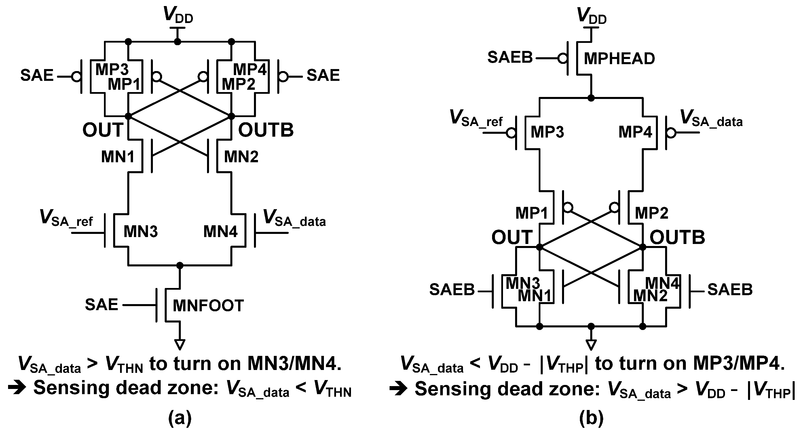
2. Problems in Conventional Latch-Type SAs

In the OCDS-SC, two SA input voltages, VSA_data and VSA_ref, are generated with a time difference due to the dual-stage sensing operation, as shown in Figure 2. In the first stage, SS1 is activated, and VSA_data generated in the OCDS-SC is introduced into the SA. In the second stage, SS2 is activated, and VSA_ref generated in the OCDS-SC is introduced into the SA. However, because of the time-difference input, a capacitive-coupling problem occurs when a conventional voltage-latched SA (VLSA) is used. Figure 3 shows the capacitive-coupling problem in the VLSA in which VSA_ref changes VSA_data to some extent (Δ) through parasitic capacitors. This problem increases σSA_OS from 20 mV to 30–50 mV, depending on the ratio of the output loading capacitance to the parasitic capacitance. Thus, the SA for the OCDS-SC should not be a VLSA type to avoid the capacitive-coupling problem.
Because VSA_data is generated at the operating point between a load PMOS and a clamp NMOS [11,12], the voltage range of VSA_data is from almost GND (in state 0) to almost VDD (in state 1), depending on the sensing time and process variation. Thus, a conventional current-latched SA (CLSA) with a sensing dead zone cannot be applied to the OCDS-SC to achieve a supply-rail sensing capability. Figure 4 shows the sensing-dead-zone problem in a CLSA with an NMOS footswitch (FS-CLSA) and a CLSA with a PMOS headswitch (HS-CLSA) [7]. In the FS-CLSA, the input transistors (MN3 and MN4) should be turned on for correct operation, which means that VSA_data should be greater than VTHN, where VTHN is the NMOS threshold voltage. Thus, the sensing dead zone of the FS-CLSA becomes VSA_data < VTHN. In the same manner, the sensing dead zone of the HS-CLSA becomes VSA_data > VDD − |VTHP|, where VTHP is the PMOS threshold voltage.

3. Proposed OCZS-SA

In this section, we propose the OCZS-SA that offers two major advantages of offset voltage cancellation and zero sensing dead zone.

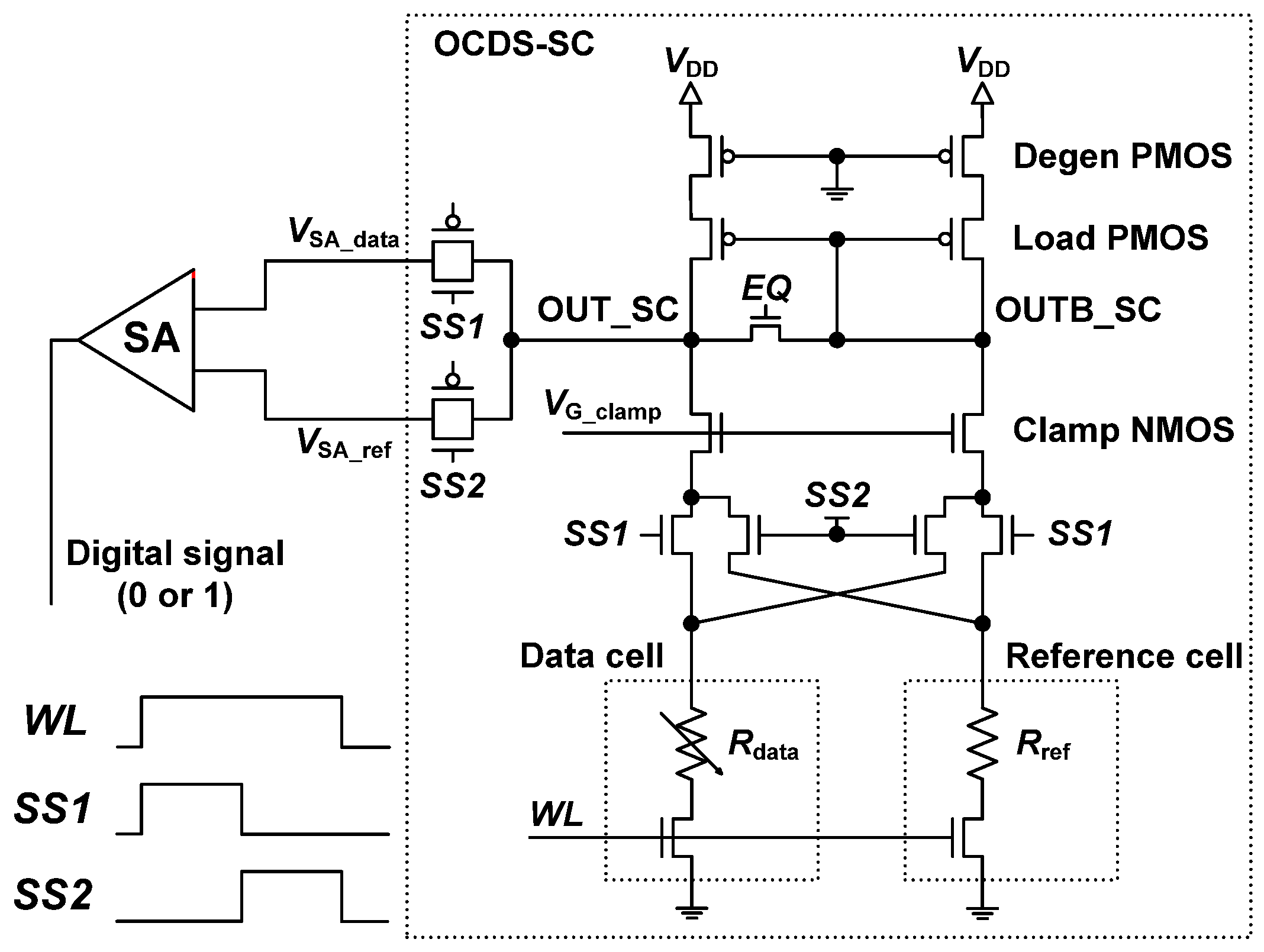
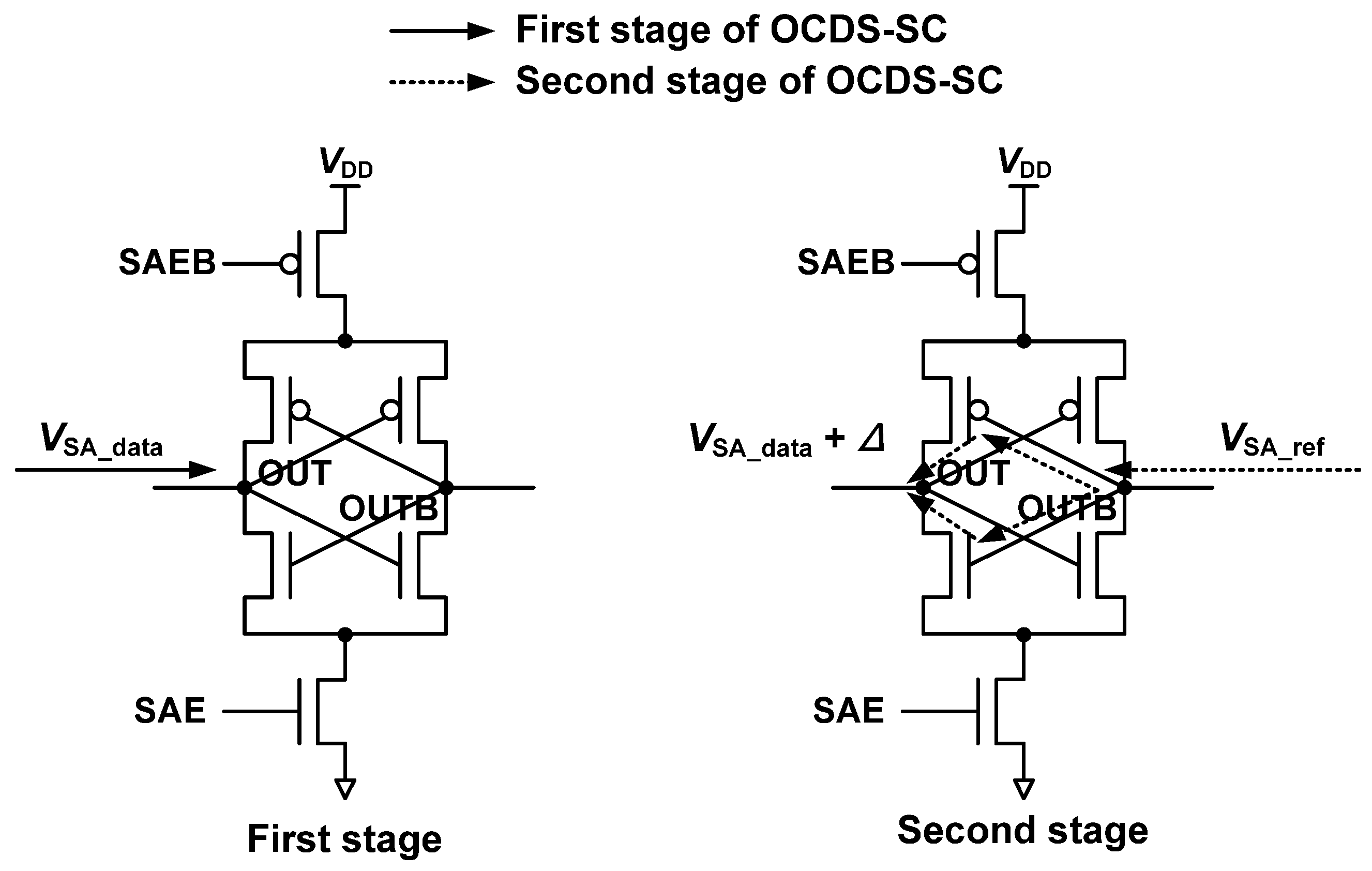
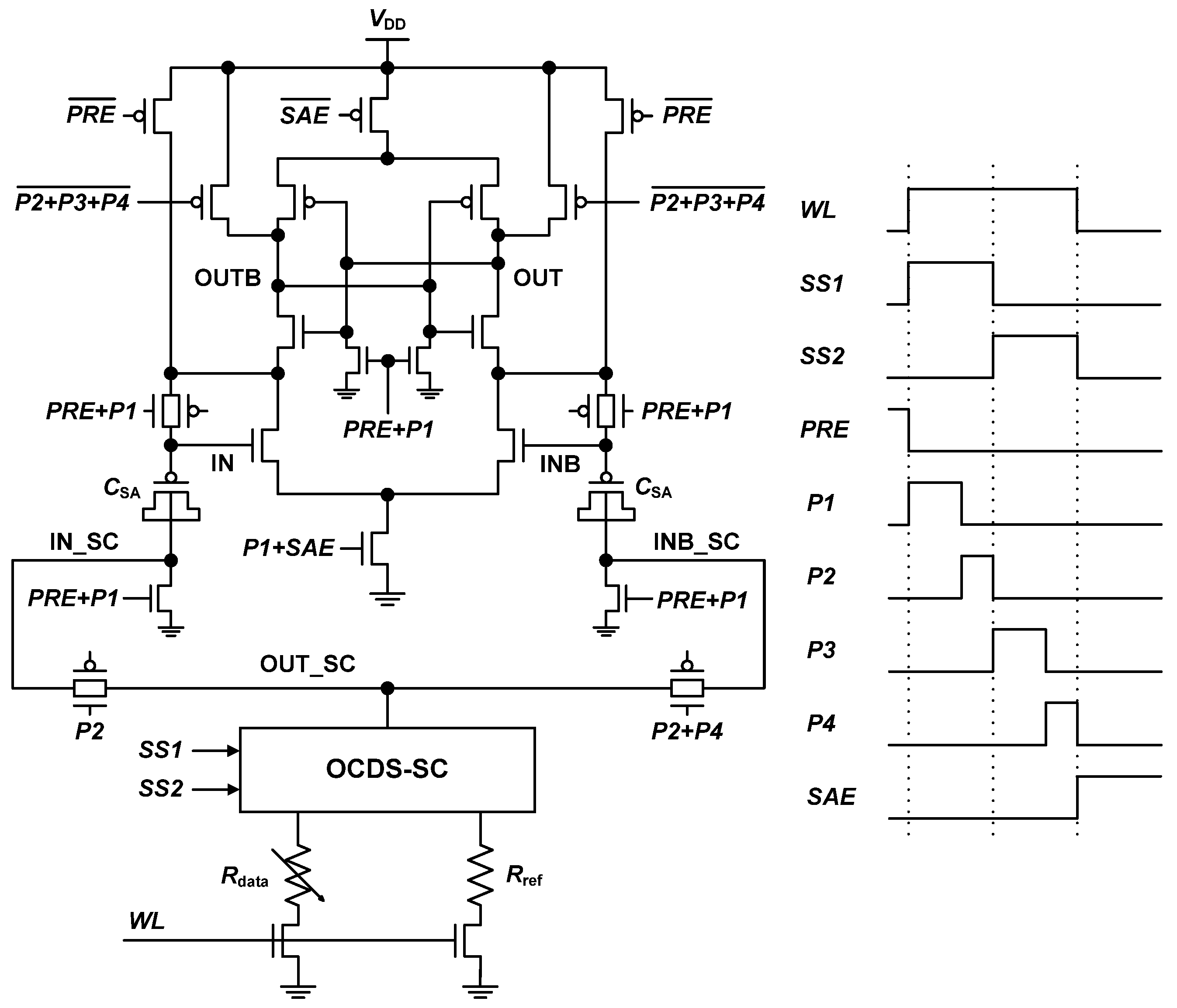
3.1. Circuit Diagram and Operation

Figure 5 shows the schematic and timing diagrams of the proposed OCZS-SA. Before we explain the OCZS-SA operation in detail, we should note that the OCZS-SA operation is fully pipelined with the OCDS-SC operation, as shown in the timing diagram in Figure 5. Phases 1 and 2 of the OCZS-SA are pipelined during SS1, and phases 3 and 4 are pipelined during SS2. Thus, the OCZS-SA does not incur any sensing delay penalty.
Figure 6 shows the detailed operations of the OCZS-SA. Before phase 1, the PRE signal is high, and the gates of the input NMOSs (IN and INB) are precharged to VDD. During phase 1 (Figure 6a), the P1 signal is activated, and the IN and INB nodes are discharged to threshold voltages VTH1 and VTH2 of the input NMOSs, respectively, by the diode-connected configuration. The OUT and OUTB nodes remain GND to isolate the IN and INB nodes. In phase 2 (Figure 6b), the P2 signal is activated, and VSA_data is captured at both the IN and INB nodes by the capacitive coupling of CSAs. As a result, the voltages in the IN and INB nodes become VTH1 + VSA_data and VTH2 + VSA_data, respectively. Simultaneously, the OUT and OUTB nodes are precharged to VDD for reliable sensing operation. In phase 3 (Figure 6c), the P3 signal is activated, and the OCZS-SA waits for VSA_ref to be generated in the OCDS-SC. In phase 4 (Figure 6d), the P4 signal is activated, and VSA_ref is captured at the INB node. Thus, the voltages in the IN and INB nodes VIN and VINB become VTH1 + VSA_data and VTH2 + VSA_ref, respectively. After phase 4, the SAE signal is activated, and a digital signal (zero or one) is generated by the voltage difference between VIN (= VTH1 + VSA_data) and VINB (= VTH2 + VSA_ref). We note that the operation after phase 4 is the same as that in the FS-CLSA.

3.2. First Advantage: Offset Voltage Cancellation

The first advantage of the OCZS-SA is the offset voltage cancellation of the two input NMOSs. As mentioned earlier, in phase 4, VIN and VINB become VTH1 + VSA_data and VTH2 + VSA_ref, respectively. Because the overdrive voltage (= VGSVTH) of the input NMOS, where VGS is the input NMOS gate-to-source voltage, does not depend on the VTH variation, a VTH mismatch between the two input NMOSs does not influence σSA_OS.
In addition, in the FS-CLSA (Figure 4a), because σSA_OS is dominantly determined by the input NMOSs, σSA_OS can be effectively reduced by canceling only the offset in the input NMOSs. Figure 7 shows σSA_OS of the FS-CLSA according to the SA input voltage (VSA_data) when process variation is applied only to the input NMOSs (MN3 and MN4), only to the latch NMOSs (MN1 and MN2), only to the latch PMOSs (MP1 and MP2), and to all the transistors. Figure 7 clearly shows that σSA_OS is more sensitive to the input NMOSs than to the transistors because the input NMOSs operate in the saturation region, whereas the latch NMOSs operate in the linear region. Thus, the VTH mismatch between MN1 and MN2 becomes less sensitive. Meanwhile, the latch PMOSs do not operate at the initial sensing period. Thus, the VTH mismatch between MP1 and MP2 becomes negligible. The variation in the latch NMOSs of the FS-CLSA has more effect on the σSA_OS as VSA_data increases because the initial voltage in the small parasitic capacitance between MN1 (MN2) and MN3 (MN4) is discharged much faster with increasing VSA_data, resulting in the latch NMOSs operating in the saturation region.

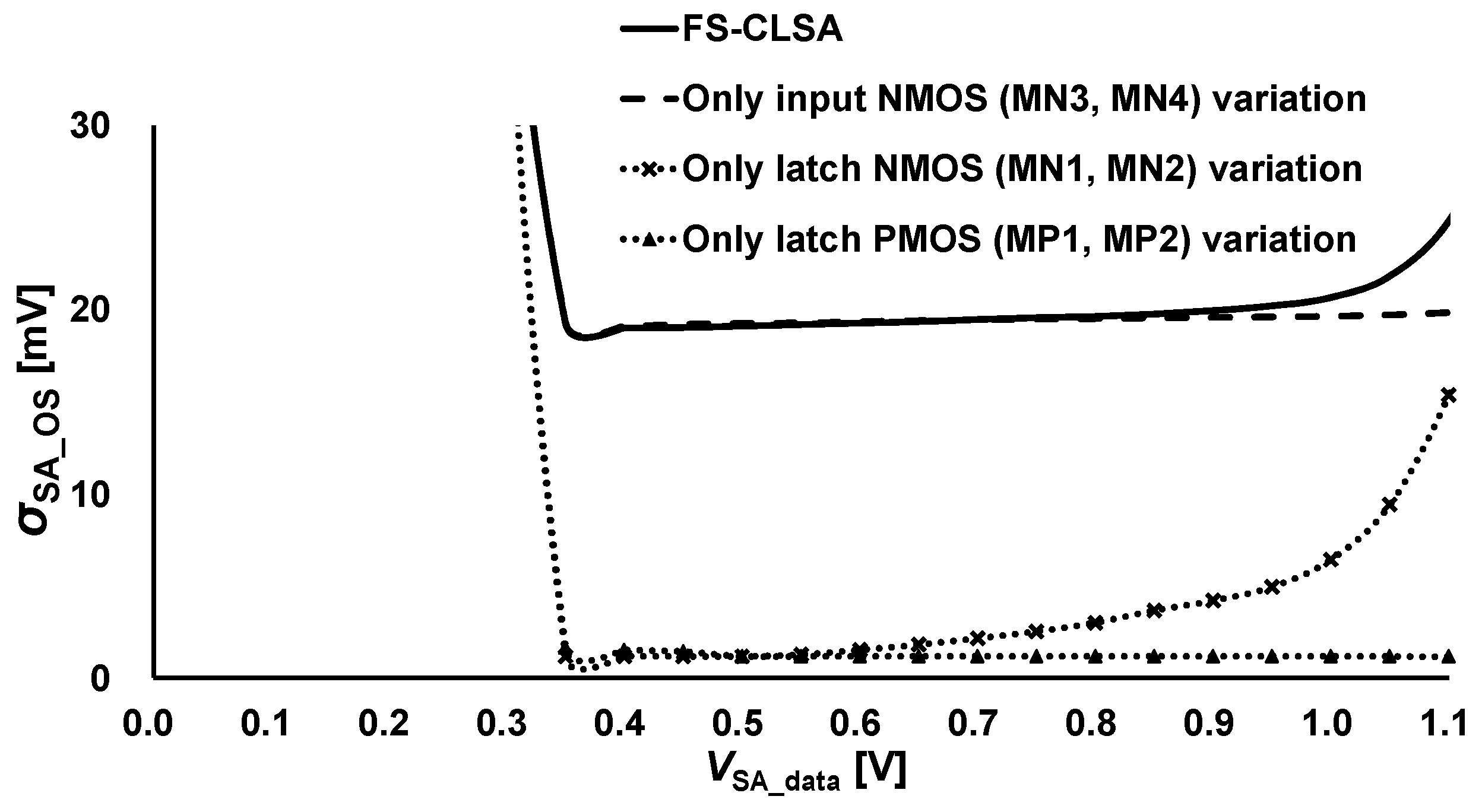
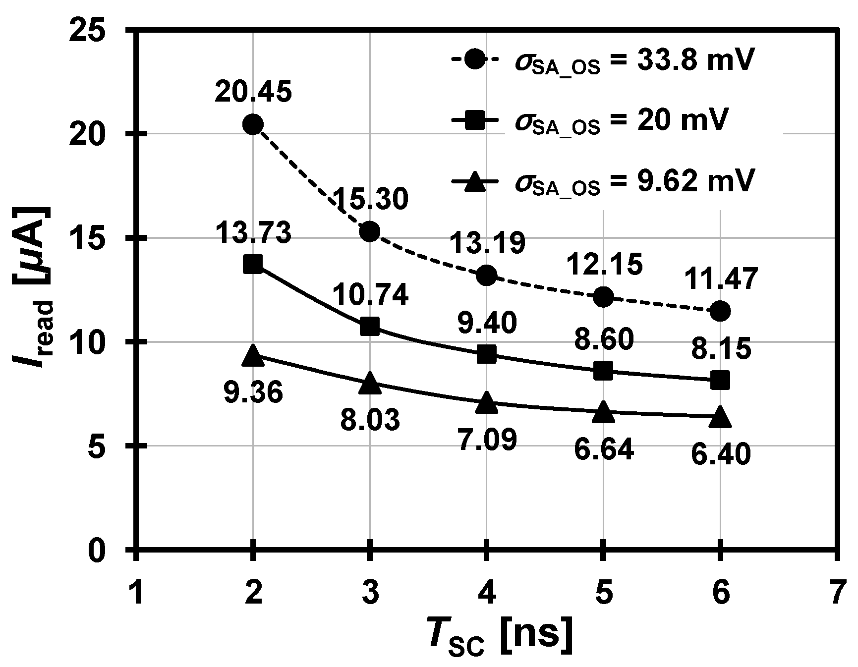
3.3. Second Advantage: Zero Sensing Dead Zone

Unlike the FS-CLSA with a sensing dead zone in the region of VSA_data < VTHN, as shown in Figure 7, the OCZS-SA does not have any sensing dead zone because in phase 4, VIN and VINB are always greater than VTH1 and VTH2, respectively, even if VSA_data and VSA_ref are 0 V. Thus, supply-rail sensing capability is achieved.

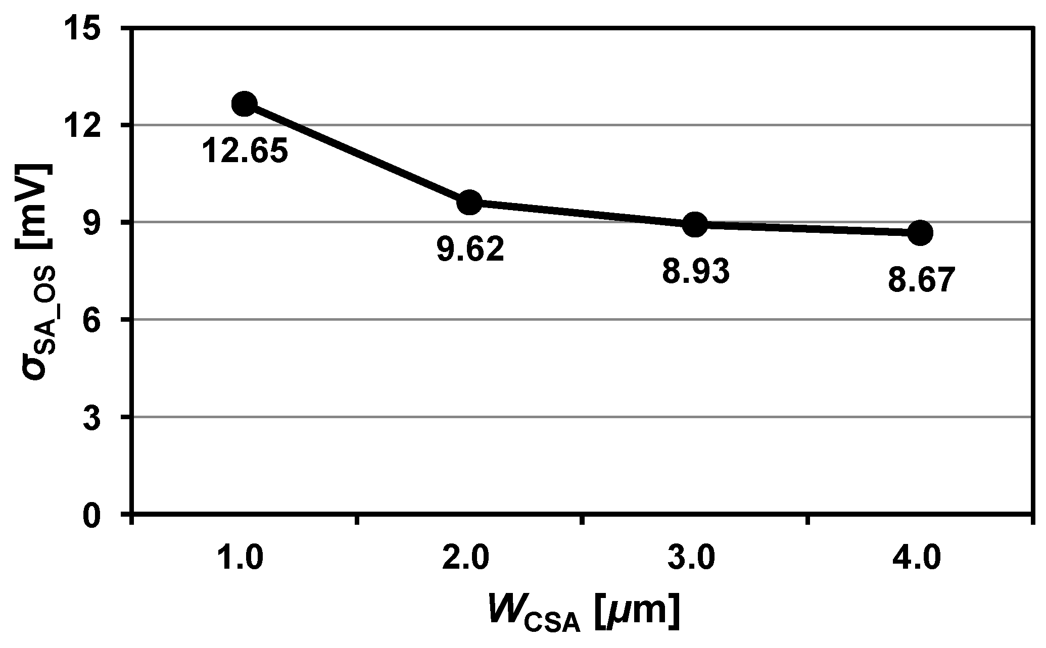
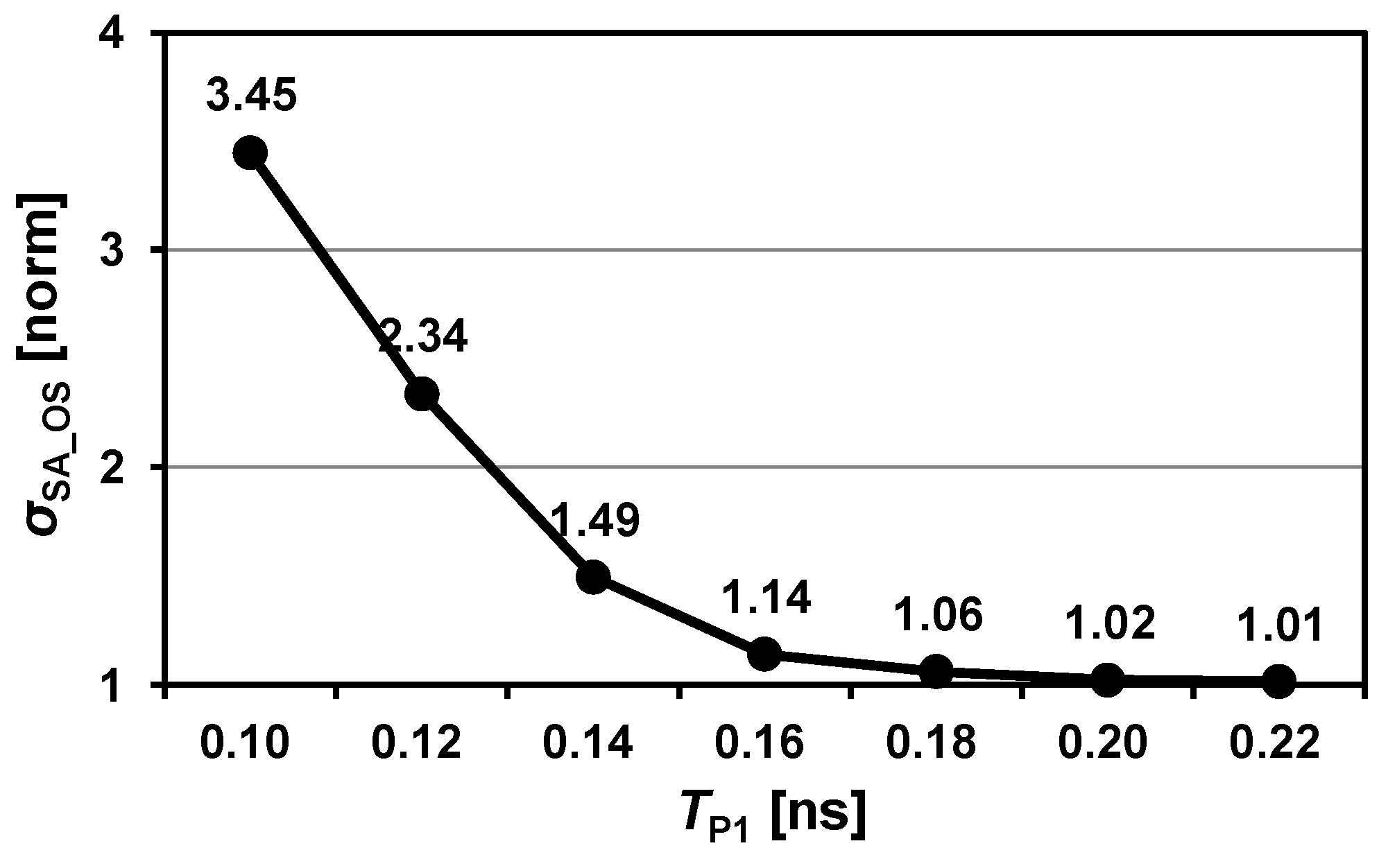
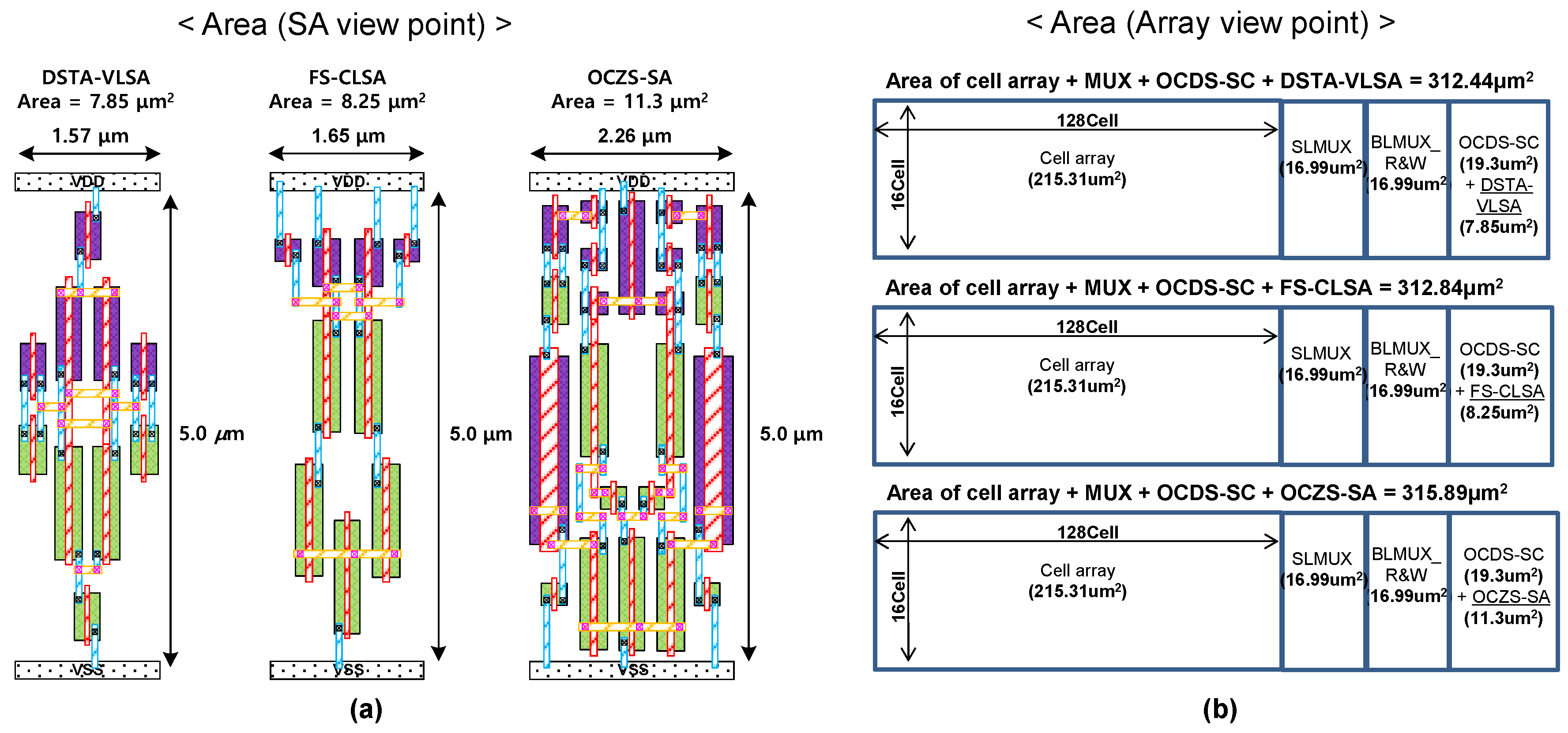
4. Simulation Results and Comparison

HSPICE Monte Carlo simulations were performed using a 65-nm predictive technology model at VDD = 1.1 V. To fully pipeline the operation with the OCDS-SC, each phase operation time (TP1, TP2, TP3, and TP4 for phases 1–4, respectively) was set to 0.5 ns.
Figure 8 shows σSA_OS according to the SA input voltage (VSA_data) of the FS-CLSA, HS-CLSA, VLSA with double switches and transmission gate access transistors (DSTA-VLSA) without time-difference inputs, DSTA-VLSA with time-difference inputs, and OCZS-SA. Among the various VLSAs such as the VLSA with an NMOS footswitch and PMOS access transistors, VLSA with a PMOS headswitch and NMOS access transistors, and DSTA-VLSA, only the latter is compared in this paper because only the DSTA-VLSA can achieve a zero sensing dead zone [7]. As mentioned in Section 2, the capacitive-coupling problem increases σSA_OS of the DSTA-VLSA when time-difference inputs are applied to the DSTA-VLSA. The FS-CLSA and HS-CLSA suffer from the sensing-dead-zone problem. On the other hand, Figure 8 clearly shows that the OCZS-SA achieved 2.1 times smaller σSA_OS of 9.62 mV on average (minimum σSA_OS = 5.07 mV at VSA_data = 0.3 V; maximum σSA_OS = 25.41 mV at VSA_data = 1.1 V) with a zero sensing dead zone. In the same manner as that of the FS-CLSA, the variation in the latch NMOSs of the OCZS-SA significantly affected σSA_OS as VSA_data increased. Thus, σSA_OS tended to increase with VSA_data.
Figure 9 shows the average σSA_OS of the OCZS-SA according to the width of the PMOSCAP for CSA (WCSA) when the PMOSCAP length (LCSA) was 0.2 μm. By considering the area overhead, a WCSA value of 2.0 μm was selected. We note that the effect of the CSA size on the loading of the OCDS-SC is negligible because CSA was serially coupled to the input capacitance (CIN) at nodes IN and INB (total loading capacitance = CSA//CINCIN).
Figure 10 shows normalized σSA_OS of the OCZS-SA according to TP1. Because σSA_OS is saturated at TP1 of approximately 0.2 ns, the OCZS-SA can be fully pipelined without any problem.
Table 1 lists the performance summary and comparison between the proposed OCZS-SA and the conventional latch-type SAs. The OCZS-SA achieved a zero sensing dead zone and a 2.1 times smaller σSA_OS of 9.62 mV, on average, than the FS-CLSA. From the SA viewpoint, owing to the additional transistors and phases, the OCZS-SA requires 37% more layout area (Figure 11a) and 125% more read energy compared with the FS-CLSA. From the array architecture viewpoint, however, the area overhead is only 1.0% when the subarray size is 128 × 16 (Figure 11b), and it decreases as the subarray size increases. In addition, the read-energy consumption of the SC part is much greater (>70 fJ [6]) than that of the SA part. As a result, if RAPYCELL, which is improved by employing the OCZS-SA, is greater than a target RAPYCELL, the total read energy in the SC and SA can be saved by reducing the SC operation time (TSC) and/or Iread. This result can be achieved in spite of the higher read energy of the OCZS-SA, which sacrifices some of the improvement in RAPYCELL but satisfies target RAPYCELL. By employing the OCZS-SA together with the OCDS-SC, RAPYCELL increases from 6.0σ to 8.7σ. The RAPYCELL values of 6.0σ and 8.7σ correspond to sensing error rates of 9.87 × 10⁻¹⁰ and 1.66 × 10⁻¹⁸, respectively. Therefore, the OCZS-SA yields an eighth-order improvement in the read yield relative to the conventional SAs.
Figure 12 shows that the minimum Iread that satisfies a target RAPYCELL value of 6σ is reduced by 21–32% by sacrificing the improvement in RAPYCELL. Figure 13 shows that the read energy in the SC and SA is accordingly reduced by approximately 13–16%.

5. Conclusions

The conventional latch-type SAs cannot be applied to the OCDS-SC due to the capacitive-coupling and sensing-dead-zone problems. In this paper, we have proposed the OCZS-SA, which offers two major advantages: offset voltage cancellation and zero sensing dead zone. The simulation results prove that the OCZS-SA can achieve a 2.1 times smaller σSA_OS value of 9.62 mV without any sensing dead zone at the cost of an increased area overhead of 1.0% for a subarray size of 128 × 16. Furthermore, a 13–16% read-energy saving is achieved due to the 21–32% reduction in Iread. Thus, the OCZS-SA can be a compelling candidate for the OCDS-SC in deep submicrometer resistive NVMs.

Funding

This work was supported by Incheon National University Research Grant in 2020.

Conflicts of Interest

The author declares no conflict of interest.

References

  1. Kawahara, A.; Azuma, R.; Ikeda, Y.; Kawai, K.; Katoh, Y.; Hayakawa, Y.; Tsuji, K.; Yoneda, S.; Himeno, A.; Shimakawa, K.; et al. An 8 Mb Multi-Layered Cross-Point ReRAM Macro With 443 MB/s Write Throughput. IEEE J. Solid State Circuits 2012, 48, 178–185. [Google Scholar] [CrossRef]
  2. Lin, C.; Kang, S.; Wang, Y.; Lee, K.; Zhu, X.; Li, X.; Hsu, W.; Kao, Y.; Liu, M.; Chen, W.; et al. 45nm low power CMOS logic compatible embedded STT MRAM utilizing a reverse-connection 1T/1MTJ cell. IEEE Int. Electron Devices Meet. (IEDM) 2009, 1–4. [Google Scholar] [CrossRef]
  3. Rizzo, N.D.; Houssameddine, D.; Janesky, J.; Whig, R.; Mancoff, F.B.; Schneider, M.L.; de Herrera, M.; Sun, J.J.; Nagel, K.; Deshpande, S.; et al. A Fully Functional 64 Mb DDR3 ST-MRAM Built on 90 nm CMOS Technology. IEEE Trans. Magn. 2013, 49, 4441–4446. [Google Scholar] [CrossRef]
  4. Chang, M.-F.; Shen, S.-J.; Liu, C.-C.; Wu, C.-W.; Lin, Y.-F.; King, Y.-C.; Lin, C.-J.; Liao, H.-J.; Chih, Y.-D.; Yamauchi, H. An Offset-Tolerant Fast-Random-Read Current-Sampling-Based Sense Amplifier for Small-Cell-Current Nonvolatile Memory. IEEE J. Solid State Circuits 2013, 48, 864–877. [Google Scholar] [CrossRef]
  5. Na, T.; Kim, J.; Kim, J.P.; Kang, S.H.; Jung, S.-O. Reference-Scheme Study and Novel Reference Scheme for Deep Submicrometer STT-RAM. IEEE Trans. Circuits Syst. I Regul. Pap. 2014, 61, 3376–3385. [Google Scholar] [CrossRef]
  6. Na, T.; Kim, J.; Kim, J.P.; Kang, S.H.; Jung, S.-O. A Double-Sensing-Margin Offset-Canceling Dual-Stage Sensing Circuit for Resistive Nonvolatile Memory. IEEE Trans. Circuits Syst. II Express Briefs 2015, 62, 1109–1113. [Google Scholar] [CrossRef]
  7. Na, T.; Woo, S.-H.; Kim, J.; Jeong, H.; Jung, S.-O. Comparative Study of Various Latch-Type Sense Amplifiers. IEEE Trans. Very Large Scale Integr. (VLSI) Syst. 2013, 22, 425–429. [Google Scholar] [CrossRef]
  8. Nho, H.; Yoon, S.-S.; Wong, S.; Jung, S.-O. Numerical Estimation of Yield in Sub-100-nm SRAM Design Using Monte Carlo Simulation. IEEE Trans. Circuits Syst. II Express Briefs 2008, 55, 907–911. [Google Scholar] [CrossRef]
  9. Na, T.; Kim, J.; Kim, J.P.; Kang, S.H.; Jung, S.-O. An Offset-Canceling Triple-Stage Sensing Circuit for Deep Submicrometer STT-RAM. IEEE Trans. Very Large Scale Integr. (VLSI) Syst. 2014, 22, 1620–1624. [Google Scholar] [CrossRef]
  10. Na, T.; Kim, J.P.; Kang, S.H.; Jung, S.-O. Read Disturbance Reduction Technique for Offset-Canceling Dual-Stage Sensing Circuits in Deep Submicrometer STT-RAM. IEEE Trans. Circuits Syst. II Express Briefs 2016, 63, 578–582. [Google Scholar] [CrossRef]
  11. Kim, J.; Ryu, K.; Kang, S.H.; Jung, S.-O. A Novel Sensing Circuit for Deep Submicron Spin Transfer Torque MRAM (STT-MRAM). IEEE Trans. Very Large Scale Integr. (VLSI) Syst. 2010, 20, 181–186. [Google Scholar] [CrossRef]
  12. Na, T.; Kang, S.H.; Jung, S.-O. Distribution Analysis and Multiple-point Tail Fitting Yield Estimation Method for STT-MRAM. J. Semicond. Technol. Sci. 2020, 20, 271–280. [Google Scholar] [CrossRef]
Figure 1. (a) Example of ΔV distribution of the offset-canceling dual-stage sensing circuit (OCDS-SC) at μV = 200 mV and σV = 23 mV. (b) RAPYCELL according to σSA_OS.
Electronics 09 01403 g001
Figure 2. Schematics of the OCDS-SC and symbolized sense amplifier (SA).
Electronics 09 01403 g002
Figure 3. Capacitive coupling problem when voltage-latched SA (VLSA) is used.
Electronics 09 01403 g003
Figure 4. Sensing-dead-zone problem when current-latched SAs (CLSAs) are used in cases of (a) footswitch (FS)-CLSA and (b) headswitch (HS)-CLSA.
Electronics 09 01403 g004
Figure 5. Schematic and timing diagrams of the proposed offset-canceling zero-sensing-dead-zone SA (OCZS-SA).
Electronics 09 01403 g005
Figure 6. Operations of the OCZS-SA in (a) phase 1, (b) phase 2, (c) phase 3, and (d) phase 4.
Electronics 09 01403 g006
Figure 7. σSA_OS of the FS-CLSA according to the SA input voltage (VSA_data) when the process variation is applied only to the input NMOSs (MN3 and MN4), only to the latch NMOSs (MN1 and MN2), only to the latch PMOSs (MP1 and MP2), and to all transistors.
Electronics 09 01403 g007
Figure 8. σSA_OS according to the SA input voltage (VSA_data) for FS-CLSA, HS-CLSA, DSTA-VLSA without time-different inputs, DSTA-VLSA with time-difference inputs, and OCZS-SA. The OCZS-SA achieves σSA_OS of 9.62 mV on average (minimum σSA_OS = 5.07 mV at VSA_data = 0.3 V; maximum σSA_OS = 25.41 mV at VSA_data = 1.1 V).
Electronics 09 01403 g008
Figure 9. Average σSA_OS of the OCZS-SA according to WCSA when LCSA = 0.2 μm.
Electronics 09 01403 g009
Figure 10. Normalized σSA_OS of the OCZS-SA according to TP1.
Electronics 09 01403 g010
Figure 11. (a) Simplified layouts of DSTA-VLSA, FS-CLSA, and OCZS-SA. (b) Estimated array architecture areas when DSTA-VLSA, FS-CLSA, and OCZS-SA are employed.
Electronics 09 01403 g011
Figure 12. Minimum Iread of the OCDS-SC that satisfies a target RAPYCELL of 6σ according to TSC at σSA_OS values of 33.8 mV, 20 mV, and 9.62 mV.
Electronics 09 01403 g012
Figure 13. Normalized read energy per bit according to TSC in cases of OCDS-SC + DSTA-VLSA, OCDS-SC + FS-CLSA, and OCDS-SC + OCZS-SA.
Electronics 09 01403 g013
Table 1. Performance summary and comparison between the proposed OCZS-SA and conventional latch-type SAs.
DSTA-VLSAFS-CLSAOCZS-SA
Average σSA_OS (mV)33.8 1)20.0 2)9.62
Sensing dead zoneNoneVSA_data < VTHNNone
Normalized area overhead
(SA viewpoint)
0.9511.37
Normalized area overhead
(Array viewpoint)
0.99911.010
Normalized read energy/bit
(SA viewpoint)
0.9412.25
Normalized read energy/bit 3)
(SC + SA viewpoint)
1.4310.84
1) Due to the capacitive coupling problem. 2) Sensing dead zone is not included. 3) Read energy when the minimum Iread that satisfies a target RAPYCELL of 6σ is applied at TSC = 2 ns.

