Article

A 2.4 GHz 20 W 8-channel RF Source Module with Solid-State Power Amplifiers for Plasma Generators

Department of Electronics and System Engineering, Hanyang University, Ansan 15588, Korea
*
Author to whom correspondence should be addressed.
Electronics 2020, 9(9), 1378; https://doi.org/10.3390/electronics9091378
Submission received: 29 June 2020 / Revised: 18 August 2020 / Accepted: 24 August 2020 / Published: 26 August 2020
(This article belongs to the Special Issue New CMOS Devices and Their Applications)

Abstract

:
This paper presents a novel multi-channel type RF source module with solid-state power amplifiers for plasma generators. The proposed module is consisted of a DC control part, RF source generation part, and power amplification part. A 2-stage power amplifier (PA) is combined with a gallium arsenide hetero bipolar transistor (GaAs HBT) as a drive PA and a gallium nitride high electron mobility transistor (GaN HEMT) as a main PA, respectively. By employing 8 channels, the proposed module secures better area coverage on the wafer during semiconductor processes such as chemical vapor deposition (CVD), etching and so on. Additionally, each channel can be maintained at a constant output power because they have a gain factor tunable by a variable gain amplifier (VGA). For that reason, it is possible to have uniform plasma density on the wafer. The operating sequence is controllable by an external DC control port. Moreover, copper–tungsten (CuW) heat spreaders were applied to prevent RF performance degradation from heat generated by the high power amplifier (HPA), and a water jacket was implemented at the bottom of the power amplification part for liquid cooling. Drawing upon the measurement results, the output power at each channel was over 43 dBm (20 W) and the drain efficiency was more than 50% at 2.4 GHz.

1. Introduction

The plasma generator is a device that supplies high-frequency output to the chamber to generate plasma in semiconductor process such as chemical vapor deposition (CVD), etching and so on [1,2]. The conventional power amplifiers for the plasma generator mainly used a magnetron in the sub-GHz band [3,4,5]. The magnetron has characteristics of high power density, high efficiency and low cost, but has disadvantages in that the system size has to be enlarged and it has a limited lifetime. In addition, as problems, there is the impossibility of phase control and frequency stability limited by the Q value of the load [6]. To overcome these problems, a solid-state power amplifier (SSPA) is emerging as an alternative. A representative having high output power characteristics like the magnetron is a GaN device. The GaN device has various characteristics such as high breakdown voltage, high electron mobility, high thermal conductivity, high efficiency characteristics and so on [7]. It is also very advantageous in terms of its small-form factor because it is possible to design it to be highly integrated with a semiconductor fabrication process in the high frequency band.
In order to become a qualified product, the plasma generator must be considered several criteria such as area coverage, uniformity, reliability and so on [8,9]. In order to satisfy these criteria, the output of the power amplifier module termination should be constant and should be able to cover wide areas on wafers. The conventional plasma generators used one or several RF sources. When using one RF source, there are problems regarding poor area coverage and non-uniform plasma density. On the other hand, when using several RF sources, the size of the plasma generator becomes large and there is a performance difference between them, so it is difficult to secure uniform plasma density.
In this paper, a 2.4 GHz 20 W 8-channel power amplifier module for plasma generators is proposed. The output termination of the proposed module consists of eight channels to satisfy the better area coverage criterion. For the uniform plasma density, moreover, output power at each channel has a distance of 4 cm intervals and can be tuned from a variable gain amplifier (VGA). In addition, the consideration of thermal management such as a heat spreader and liquid cooling were implemented in the proposed PA module to prevent performance degradation due to high power density. The paper is organized as follows: Section 2 describes what kind of components are considered and how to design the proposed module. In Section 3, the implemented module, experimental conditions, and equipment used for measurement are presented and the RF measurement results are shown under test conditions. Furthermore, a discussion is presented about the proposed module. Finally, in Section 4, the conclusions are presented.

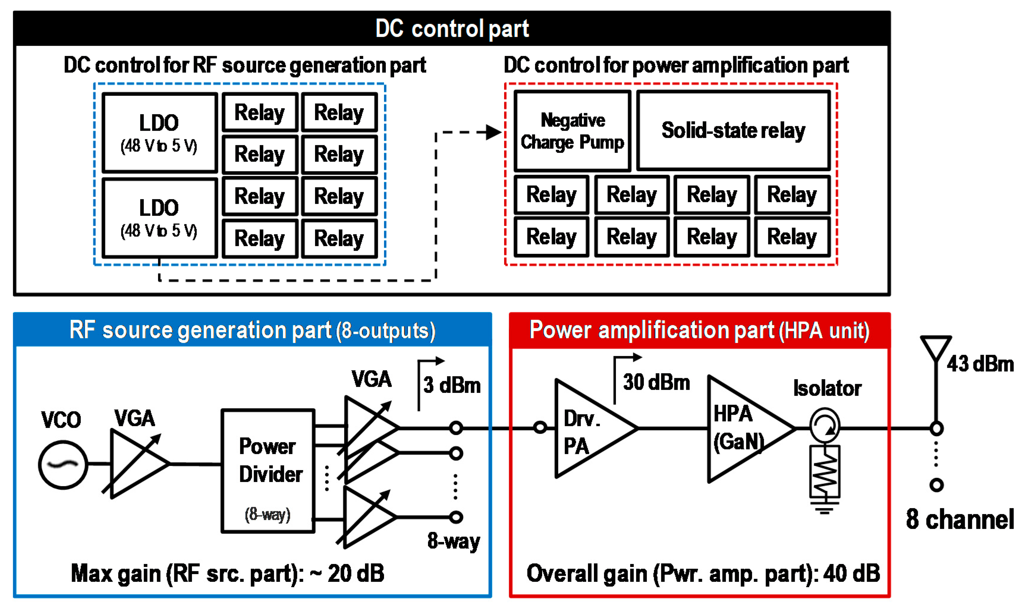
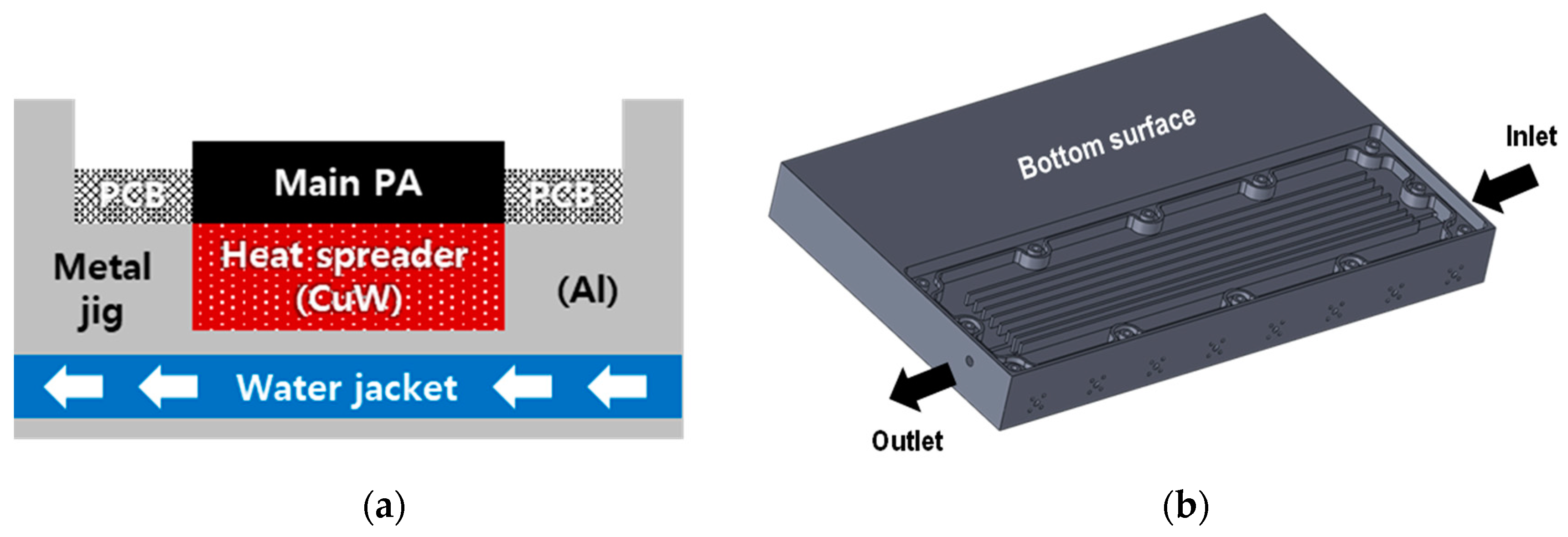
2. Design of the Proposed Power Amplifier Module

As shown in Figure 1, the proposed module is divided into three parts which include the DC control part, RF source generation part and power amplification part. The DC control part provides DC supply and control for safe operation of the RF source generation part and power amplification part. As shown in Table 1, there are five DC control biases required for the proposed module, and the rest of DC source, except 48 V, is used as a control for the module operation. The proposed module needs 48 V for DC feeding and 5 V for control, and its operation is determined according to the 5 V input sequence. This sequence comes from the characteristics of the GaN device of the main PA. When the gate is floating, the GaN device is in normally in the on state, so applying drain bias under the condition causes a lot of drain current and will damage the transistor. Relays are used at each location to control module operation and the operation process should be followed sequentially as shown in Table 2. The process of turning off is in the reverse order of turning on. In this part, there are several components used as follows: the solid-state relay (SSR) is the CMX60D20 (Crydom), the low dropout regulators (LDO)s are TPS54560DDAR (Texas Instrument), the relays are 8L01-05-111, 8L61-05-111 (Coto technology), and a negative charge pump is MAX889 (MAXIM).
Sequence 1 
(Off-state): when 48 V of the main DC bias is applied first, it is converted from 48 V to 5 V through the low dropout regulator (LDO) and supplied to a voltage controlled oscillator (VCO), variable gain amplifier (VGA), drive PA, negative charge pump and so on. In addition, some are converted to negative voltage through a negative charge pump. Because the transistors have to be ensured to be in the off state before applying drain bias, −5 V is applied as the gate bias of the main PA.
Sequence 2 
(Ideal state #1): VSSR_EN of the solid-state relay (SSR) is turned on to supply 48 V DC bias to the drain of the main PA.
Sequence 3 
(Ideal state #2): VHPA_EN and VDRV_EN are activated to turn the main PA and drive PA on, respectively.
Sequence 4 
(Power emission): when VSRC_EN is activated to make the VCO switch to the on state, the proposed module generates 20 W output power at each channel.
The RF source generation part consists of a VCO to generate a 2.4 GHz RF signal and VGAs to provide sufficient gain for the power amplification part, and the 8-way divider combined of 3 stages of 2-way dividers to implement 8 channels. The 8-way divider design is so important to minimize the phase unbalance between each channel. The phase unbalance of commercial 2-way dividers is provided as 0.58 degrees based on the datasheet and the measurement data value of a unit 2-way divider module was 0.219 degrees. To implement the 8-way divider, three 2-way dividers and a transmission line were utilized, the structure of transmission line was optimized in order to minimize phase unbalance. Figure 2a shows the phase simulation data at each channel, and the difference between minimum and maximum value is 3.943 degrees. From Figure 2b, the difference between minimum and maximum value is 2.001 degrees based on measurement data, so the phase difference among channels is within 5 degrees. The phase unbalance is caused by the length of the transmission line connected to be evenly divided into each channel, and the phase unbalance of the 2-way divider overlaps up to three times when configured in 8 ways.
When the VCO generates a 2.4 GHz −3 dBm signal, the first VGA amplifies the signal. After passing through the 8-way divider, the signal is amplified to 3 dBm through the second VGA of each channel so that it can be transmitted to the power amplification part. Each VGA uses a trimmer, a variable resistor at the top of the module, to adjust the gain for each channel, and the VCO also uses a trimmer as a correction for the output frequency when the frequency is changed. The VCO is a MAX2750EUA+ (MAXIM), the VGAs are MAX2057ETX+ (MAXIM), the 2-way dividers are GP2Y+ (Mini-Circuits), and the trimmers are 3266Y-1-104LF (BOURNS), respectively.
In the power amplification part, the input signal from the RF source generation part can be achieved as the final target 20 W output power by the 2-stage power amplifier as shown in Figure 3a. The drive PA uses VDRV_EN: 2.6 V and VDRV_CC: 5 V and amplifies the input signal to the output power of 30 dBm. The main PA uses VHPA_EN: −2.6 to −0.75 V, VHPA_DD: 48 V, and amplifies the signal as an input to a signal of 43 dBm (20 W). As a result of measuring the main stage PA test unit, the following results were obtained which are shown in Figure 3b, and it was confirmed that the target output power, more than 20 W at each channel, could be achieved when the RF source is divided into 8 channels. The proposed PA module should be designed with stability considered in order to secure reliability in operation. Since the power amplifiers are dependent on frequency and matching network, various stability analysis methods exist [10,11,12,13]. The stability was determined by Rollet’s factor, K, using network scattering parameters to prevent issues such as oscillation. Moreover, negative resistance was checked in input and output nodes. Based on the analysis methods, the stability was verified by simulation and measurement as shown in Figure 4. From comparison between simulation and measurement data, both results confirmed that K > 1 conditions were satisfied. Furthermore, there was no negative resistance in each input and output node. Furthermore, the frequency spectrum was measured through the spectrum analyzer, and it was verified that there were no harmonic spur and oscillation at target frequency. The isolators are used to prevent damage to transistors caused by reflected power from antenna mismatch. An ACPM-5040 (Avago technologies) was used as the drive PA, an RFHA3942D (RFMD) was used as the main PA, and an ADI240CET (ADMOTECH) was used as the isolator.
In the case of HPAs using GaN devices, there is a thermal management problem due to high power density characteristics. If this heat is not dissipated well, not only RF performance degradation but also severe burnout may occur. Therefore, in order to solve this problem, a heat spreader was implemented using CuW to minimize thermal deformation instead of an aluminum body at the bottom of the power amplification part as shown in Figure 5a. In addition, thermal interface material was applied between transistors and heat spreader, and between heat spreader and metal jig to maximize the contact area between each boundary. Moreover, liquid cooling, a method frequently used in system-level cooling, was applied. A water jacket was created at the bottom of the aluminum body, and a passage through which coolant could be circulated on the left and right sides was provided for continuous heat dissipation in, as shown in Figure 5b.

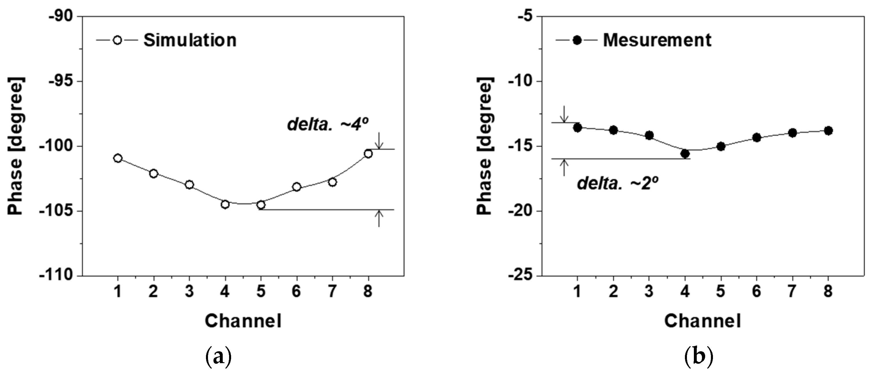
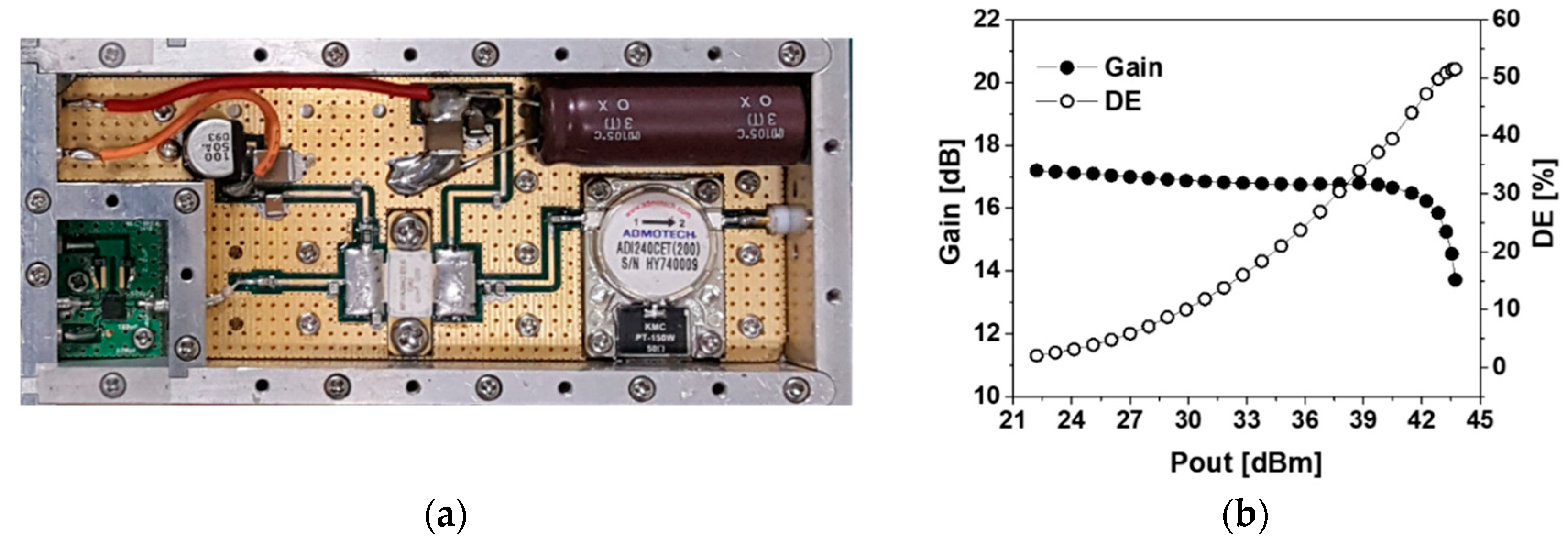
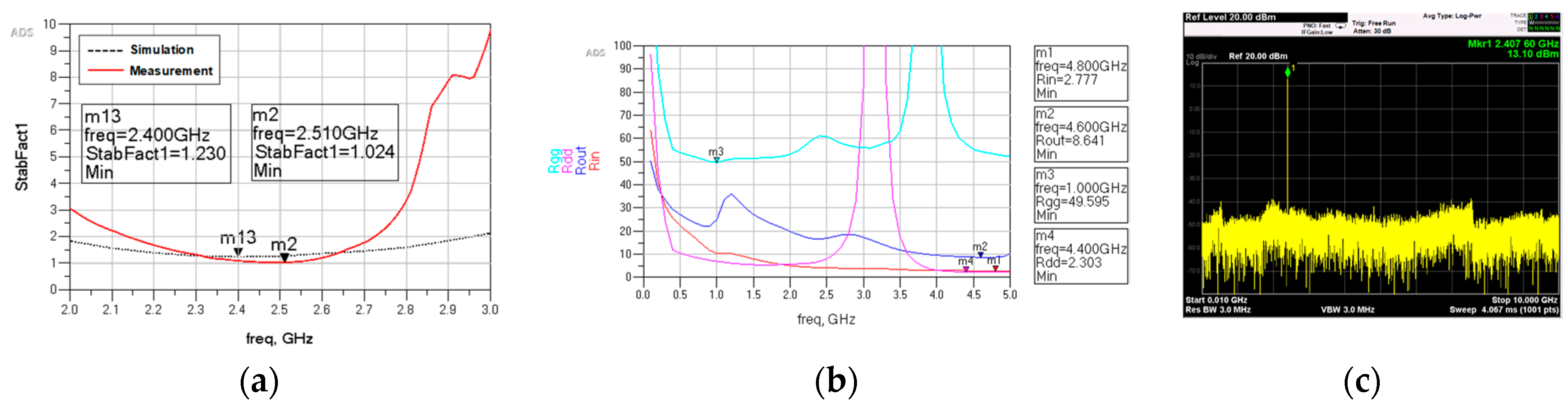
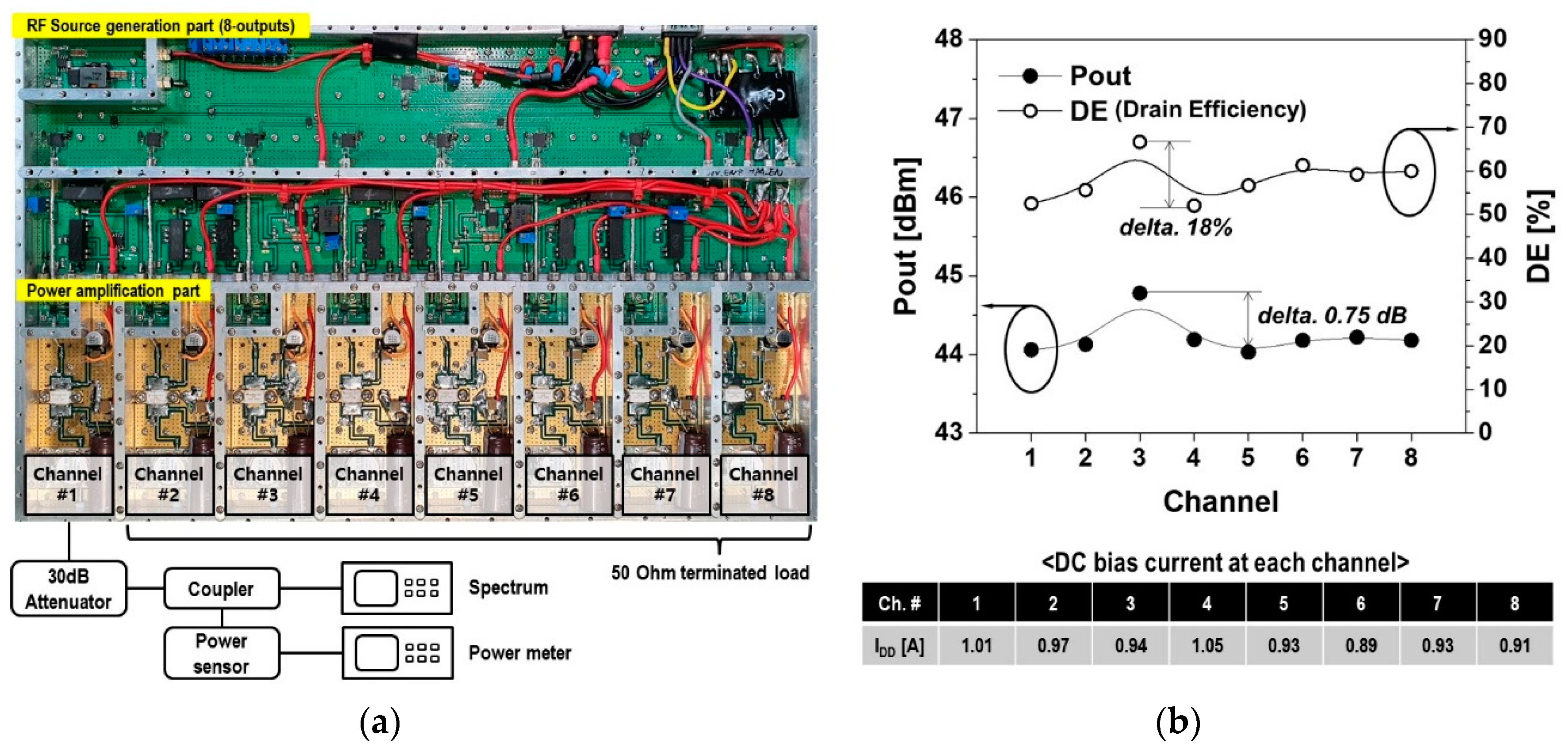
3. Measurement Results

The entire circuit mentioned in Section 2 was implemented inside an aluminum body. Figure 6a is a photograph of the proposed module and measurement setup. The total module size is 365 mm × 229 mm × 30 mm in the order of width, length, and height, respectively. Each part is divided into 5 mm bulkheads to prevent interference with each other. A printed circuit board (PCB) for the power amplification part is used (the RT-druoid 6035HTC (Rogers Cooperation)), and the others are used 4-layers FR4. As for the measurement method, seven of the eight-channels were terminated with an attenuator and 50 Ohm, after that the measurement was performed by rotating each channel. The E4417A (Agilent technologies) as a power meter, the E9323A (Agilent technologies) as a power sensor, the E4404B (Agilent technologies) as a spectrum analyzer, the N5767A (Agilent technologies) as a DC supply, and the Exos-2.5 (Koolance) as a liquid cooling system were used as the measurement equipment. The measurement environment was covered with the top plate of the module, and liquid cooling was performed at room temperature (25 °C). The RF performance was measured after aging for more than 15 min. Each channel was confirmed to have a target output power of more than 20 W (43 dBm), and 50% of drain efficiency, as shown in Figure 6b. In the case of output power, the difference between the minimum and maximum values of each channel was 0.75 dB. The output power of each channel can be further reduced by adjusting the gain of the VGAs at the RF source generation part.
In Table 3, the RF performance of the proposed module for a plasma generator is compared with other modules in plasma generator application [14,15,16,17]. Even though the proposed module shows the smallest output power compared to the others, the 8-channel construction was the first to show better area coverage and uniform plasma density. Furthermore, the low output power level is not a major disadvantage anymore. This is because it is not difficult to improve output power if more HPAs are combined and replaced depending on various applications. References [15,16,17] used multiple SSPAs to construct multi-channels for similar purposes. Two types of antennae are installed at each end of the SSPA to provide a solution by comparing plasma density according to the number of antennas, the placement interval between antennas, the plasma generation distance, and so on. Therefore, the proposed PA module has the advantage of integration of a low complexity of the system configuration because it has multiple channels in one module compared to conventional modules. In addition, each channel with output power and phase characteristics at the same level has better uniform plasma density because it is maintained at intervals of 4 cm. If two or more modules can be assembled together outside the metal jig, it is advantageous for securing more detailed and wider area coverage.
Moreover, considering the design for thermal management is another benefit compared to conventional modules. In the case of PA, the operating temperature is strongly dependent on the output power because most of the energy which cannot be converted to RF power is dissipated as heat energy. Therefore, the thermal issue becomes more serious and it results in degradation of the RF performance (output power, PAE and so on) [18]. For these reasons, heat spreader and liquid cooling were considered for implementation in the proposes PA module in order to prevent the module overheating during high power operation.

4. Conclusions

A novel 20 W 8-channel power amplifier module has been proposed for plasma generators. To achieve better area coverage, the output termination was constructed to be 8-channel. For uniform plasma density, moreover, each channel can be maintained at a constant output power, because it has a gain tunable factor in the RF source generation part. In the power amplification part, a 2-stage PA was implemented, and to each PA was applied a CuW heat spreader and liquid cooling at the bottom. The RF measurements showed that the output power was around 20 W at each channel, and the drain efficiency was more than 50%. For that reason, the proposed module presents a new possibility for improving the plasma density and area coverage of plasma generators.

Author Contributions

Conceptualization, formal analysis, investigation, and resources, H.N. and J.K.; methodology, software, validation, data curation, writing—original draft preparation, writing—review and editing, and visualization, H.N. and T.S.; supervision, project administration, and funding acquisition, J.K. All authors have read and agreed to the published version of the manuscript.

Funding

This work was supported in part by the BK21PLUS Program through the National Research Foundation of Korea within the Ministry of Education, and in part by the National Research Foundation of Korea (NRF) grant funded by the Korea government (Ministry of Science) (No. NRF—2020R1A2B5B01002400).

Conflicts of Interest

The authors declare no conflict of interest.

References

  1. Wang, Q.; Wu, G.; Liu, S.; Gan, Z.; Yang, B.; Pan, J. Simulation-Based Development of a New Cylindrical-Cavity Microwave-Plasma Reactor for Diamond-Film Synthesis. Crystals 2019, 9, 320. [Google Scholar] [CrossRef] [Green Version]
  2. Szabó, D.V.; Schlabach, S. Microwave Plasma Synthesis of Materials—From Physics and Chemistry to Nanoparticles: A Materials Scientist’s Viewpoint. Inorganics 2014, 2, 468–507. [Google Scholar] [CrossRef] [Green Version]
  3. Petreuş, D.; Grama, A.; Cadar, S.; Plaian, E.; Rusu, A. Design of a plasma generator based on E power amplifier and impedance matching. In Proceedings of the 2010 12th International Conference on Optimization of Electrical and Electronic Equipment, Basov, Romania, 20–22 May 2010; pp. 1317–1322. [Google Scholar]
  4. Miotk, R.; Jasinski, M.; Mizeraczyk, J. Optimization of microwave power transfer from electric field to the plasma inside an microwave 915 MHz plasma source. In Proceedings of the 2016 International Conference on Actual Problems of Electron Devices Engineering (APEDE), Saratov, Russia, 22–23 September 2016; pp. 1–8. [Google Scholar]
  5. Miotk, R.; Jasinski, M.; Mizeraczyk, J. Improvement of Energy Transfer in a Cavity-Type 915-MHz Microwave Plasma Source. IEEE Trans. Microw. Theory Tech. 2017, 66, 711–716. [Google Scholar] [CrossRef]
  6. Pengelly, R.S.; Wood, S.M.; Milligan, J.W.; Sheppard, S.T.; Pribble, W.L. A Review of GaN on SiC High Electron-Mobility Power Transistors and MMICs. IEEE Trans. Microw. Theory Tech. 2012, 60, 1764–1783. [Google Scholar] [CrossRef]
  7. Horikoshi, S.; Serpone, N. (Eds.) RF Power Semiconductor Generator Application in Heating and Energy Utilization; Springer Nature: Singapore, 2020; pp. 25–39, 181–194. [Google Scholar]
  8. Chen, F.F.; Chang, J.P. Lecture Notes on Principles of Plasma Processing; Springer Science and Business Media: New York, NY, USA, 2003; pp. 25–30. [Google Scholar]
  9. Wu, R.; Benqing, G.; Zhenghui, X.; Weiming, L. The study of the rf field in a plasma reactor. In Proceedings of the Cross Strait Quad-Regional Radio Science and Wireless Technology Conference (CSQRWC) 2012, New Taipei City, Taiwan, 23–27 July 2012; pp. 191–194. [Google Scholar]
  10. Pozar, D.M. Microwave Engineering, 4th ed.; Wiley: Hoboken, NJ, USA, 2012; pp. 564–570. [Google Scholar]
  11. Gonzalez, G. Microwave Transistor Amplifiers: Analysis and Design, 2nd ed.; Prentice Hall: Upper Saddle River, NJ, USA, 1997; pp. 217–227. [Google Scholar]
  12. Pantoli, L.; Leuzzi, G.; Santarelli, A.; Filicori, F. Stability Analysis and Design Criteria of Paralleled-Device Power Amplifiers Under Large-Signal Regime. IEEE Trans. Microw. Theory Tech. 2016, 64, 1442–1455. [Google Scholar] [CrossRef]
  13. Pantoli, L.; Leuzzi, G.; Santarelli, A.; Filicori, F.; Giofrè, R. Stabilisation approach for multi-device parallel power amplifiers under large-signal regime. In Proceedings of the 2011 6th European Microwave Integrated Circuit Conference, Manchester, UK, 10–11 October 2011; pp. 144–147. [Google Scholar]
  14. Bansleben, C.; Heinrich, W. Compact high-power high-efficiency microwave generator with differential outputs. In Proceedings of the 2014 44th European Microwave Conference, Rome, Italy, 6–9 October 2014; pp. 723–726. [Google Scholar]
  15. Korpas, P.; Gryglewski, D.; Wojtasiak, W.; Gwarek, W. A Computer-controlled System of High-power Microwave Sources. Int. J. Electron. Telecommun. 2011, 57, 121–126. [Google Scholar] [CrossRef]
  16. Latrasse, L.; Radoiu, M.; Lo, J.; Guillot, P. 2.45-GHz microwave plasma sources using solid-state microwave generators. Collisional-type plasma source. J. Microw. Power Electromagn. Energy 2017, 51, 43–58. [Google Scholar] [CrossRef]
  17. Latrasse, L.; Radoiu, M.; Lo, J.; Guillot, P. 2.45-GHz microwave plasma sources using solid-state microwave generators. ECR-type plasma source. J. Microw. Power Electromagn. Energy 2017, 50, 308–321. [Google Scholar] [CrossRef]
  18. Tong, X.C. Advanced Materials for Thermal Management of Electronic Packaging; Springer: Berlin, Germany, 2011; pp. 1–55, 305–370, 421–473. [Google Scholar]
Figure 1. The block diagram of the proposed module.
Electronics 09 01378 g001
Figure 2. The phase distribution and unbalance (a) simulation (b) measurement.
Electronics 09 01378 g002
Figure 3. (a) a photograph of two stage power amplifier (b) RF measurement results of main stage amplifier.
Electronics 09 01378 g003
Figure 4. (a) Comparison Rollet’s factor between simulation and measurement (b) Determination of negative resistance from real part of gamma (c) The measurement data of frequency spectrum from DC to 10 GHz.
Electronics 09 01378 g004
Figure 5. Cooling method consideration of the proposed module (a) the cross-sectional view of heat spreader implementation (b) the 3-D model of water jacket implementation at bottom.
Electronics 09 01378 g005
Figure 6. (a) A photograph of the proposed module and measurement setup (b) the measurement result of each channel.
Electronics 09 01378 g006
Table 1. DC control bias description.
Control BiasDC LevelDescription
Vsupply48 V, 7.63 AMain DC source
VSSR_ENhigh (5 V)
or
low (0 V)
Control bit for enabling the drain supply bias of main PAs
VHPA_ENCommon control bit for main PAs on/off
VDRV_ENCommon control bit for drive PAs on/off
VSRC_ENControl bit for RF source on/off
Table 2. The proposed module operating sequence.
SequenceVSRC_ENVDRV_ENVHPA_ENVSSR_ENDescription
1LLLLOff-state
2LLLHIdeal state #1
3LHHHIdeal state #2
4HHHHPower emission
Table 3. Comparison with RF source module with solid-state power amplifiers for plasma generators.
Ref.Freq. (GHz)Topology (Device)Pout (W)Linear Gain (dB)Eff. (%)OutputCooling System
[14]2.4Differential PA (GaN)57-471-channelNone
[15]2.452-stage PA (GaN)20025-4-channelsNone
[16]2.45-200--1-channel × N ea None
[17]2.45-200--1-channel × N ea None
This work2.42-stage PA (GaAs, GaN)20 (CW)>40>508-channelLiquid cooling

