Article

A 2.45 GHz High Efficiency CMOS RF Energy Harvester with Adaptive Path Control

College of Information and Communication Engineering, Sungkyunkwan University, Suwon 16419, Korea
*
Author to whom correspondence should be addressed.
Electronics 2020, 9(7), 1107; https://doi.org/10.3390/electronics9071107
Submission received: 20 May 2020 / Revised: 1 July 2020 / Accepted: 3 July 2020 / Published: 7 July 2020
(This article belongs to the Special Issue Analog/Digital Mixed Circuit and RF Transceiver Design)

Abstract

:
In this research work, a reconfigurable 2.45-GHz RF-DC converter realized in a 180-nm complementary metal-oxide semiconductor (CMOS) technology is proposed to efficiently harvest electromagnetic energy. The proposed circuit is composed of a low-power path rectifier, a high-power path rectifier, and an adaptive path control (APC) circuit. The APC circuit is made-up of a comparator, two switches, and an inverter. The APC circuit senses the output voltages of the low-power path and the high-power path rectifiers and generates a control signal to automatically switch the proposed circuit between the lower-power path and the high-power path operation depending upon RF input power level. The proposed circuit obtains more than 20% measured power conversion efficiency (PCE) from −6 dBm to 11 dBm input power range with maximum efficiencies of 41% and 45% at 1 and 6 dBm input powers, respectively, for 5 kΩ load resistance. In addition, the proposed circuit shows excellent performance at 900 MHz and 5.8 GHz frequencies.

1. Introduction

In the past decade, an unprecedented development has been witnessed in the field of wireless power transfer (WPT). There are two common types of WPT: (a) near-field (non-radiative) technique [1,2], and (b) far-field (radiative) technique [3,4]. In the near-field WPT, power is transferred by inductive coupling coils through magnetic field. The power transmission level of this technique ranges from micro-watt (µW) to kilo-watt (kW), and deals with the variety of applications including charging of mobile phones, smart watches, electric vehicles, and medical implants. However, the transmission distance covered by this approach is quite limited and power transfer degrades with the distance between coils [5]. Therefore, near-field technique cannot scale well in Internet-of-Things (IoT), where wireless sensor nodes receive power over wide outdoor and indoor environments [6]. On the contrary, far-field WPT technique transfers power through electromagnetic waves radiated by antenna over longer distance. Figure 1 shows the block diagram of a radio frequency (RF) energy harvesting system. An antenna receives the incoming RF signals and sends them to an off-chip π-matching network (in this paper). The π-matching network matches the antenna equivalent impedance with the input impedance of an RF-DC converter and ensures the maximum power transfer from antenna to the RF-DC converter. The RF-DC converter rectifies the RF signals and converts them into DC power. RF signals are widely used for television/radio broadcasting systems, mobile communication, Bluetooth low-energy (BLE), and Wi-Fi networks [7,8,9,10]. RF energy can be scavenged anywhere and almost anytime and its feasibility has been practically verified from hardware implementation viewpoint [11,12,13]. However, RF received power is limited because of strong path loss [5], and limited maximum allowed RF transmitted power for human health problem regulations [14]. Therefore, it is a key challenge to design a high efficient RF-DC converter, which converts RF power into DC voltages, for limited RF received power. The performance of the RF-DC converter can be estimated by its power conversion efficiency (PCE) [15]. The PCE of the RF-DC converter is the useful DC power harvested by the RF-DC converter divided by the RF input power. In this paper, RF source of 2.45 GHz is chosen for harvesting by the RF-DC converter because this source is present in abundance because of the ubiquitous deployment of wireless systems, such as Bluetooth and Wi-Fi for their high data speed [16].
A number of solutions have been reported to enhance the PCE of the RF-DC converter by compensating the threshold voltages of the rectifying devices in the RF-DC converter. An adaptive power harvester reported in [16] is composed of two differential sub-rectifiers and a control circuit. The control circuit senses the output voltages of the two sub-rectifiers and generates a control signal to switch the rectifier between series mode and parallel mode. In [17], a class-E synchronous rectifier is reported based on the time-reversal duality theory where class-E amplifier is transformed into class-E rectifier. This approach is different from other RF rectifiers which normally use voltage multiplier methods. Author in [18] presents a rectifier-booster regulator (RBR) with cross dipole antenna and full-wave matching network. The RBR converts the RF energy into dc voltage and boosts it. The resultant dc voltage is supplied to full-wave rectifier employing Cockroft-Walton charge pump and Greinacher rectifier. The circuit in [19] presents analysis, modeling, and designing of a cross-coupled rectifier based on a discrete component matching network. Authors in [20,21] report maximum power point tracking (MPPT) technique to maintain high efficiency over extended input power range by selecting optimum number of rectifier stages based on RF input power levels. The circuit reported in [22] presents a dual-band rectifier utilizing internal threshold voltage cancellation technique to have low conduction loss of the rectifying devices. Reference [23] reports four different rectifier circuits in which optimum compensation voltages for the rectifying devices are generated by sub-threshold auxiliary transistors. A self-biasing technique reported in [24] consists of an off-chip resistive network to produce compensation voltage for rectifying devices. Large resistor value required to limit the leakage current occupies large area on the chip. In [25], a dual path differential CMOS rectifier utilizing adaptive control circuit is reported. The control circuit switches the rectifier between the high-power path and the lower-power path based-on the input power level. The limitation of this approach is that each cross-coupled rectifier path uses five stages which results more power loss. Moreover, NMOS switches are in the path of RF input signal which increase the parasitic capacitance causing more power loss. The circuit implemented in [26] presents a self-compensation scheme providing individual body biasing for triple-well NMOS transistors used as rectifying devices. However, triple-well MOS transistors are not available in all CMOS processes. Authors in [27] demonstrates a differential structure with cross-coupled configuration to compensate threshold voltage of the transistors and minimizes the leakage current through rectification chain. References [28,29,30,31] report cross-connected differential rectifiers with differential custom antenna. However, a PCB balun is required by differential circuit for single-ended to differential conversion or differential antenna. This causes large area on the printed circuit board (PCB) and results in additional cost.
This research work proposes a reconfigurable CMOS RF-DC converter utilizing a low-power path and a high-power path to efficiently harvest the electromagnetic energy from the ambient environment. An adaptive path control (APC) circuit switches the RF-DC converter between the low-power path and the high-power path depending upon the input power level which results in an improved PCE over wide power range. The proposed circuit significantly improves PCE compared to the previous published works over wide power range. The rest of the paper is organized as follows: Section 2 illustrates operation principle of the proposed circuit. Section 3 describes the sub-blocks used in the proposed architecture. Section 4 presents the measurement results. Finally, Section 5 discusses the conclusion of the paper.

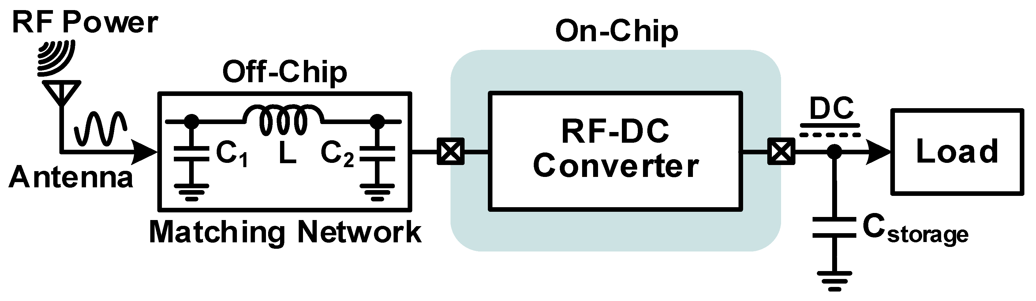
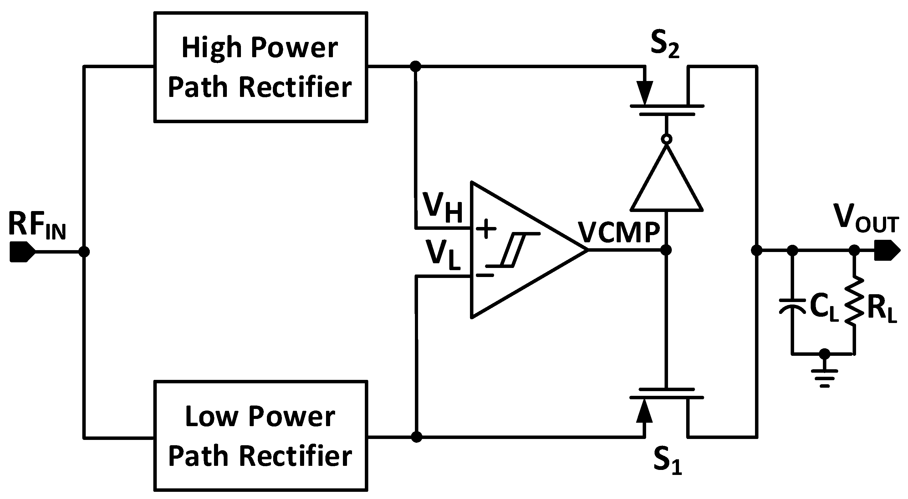
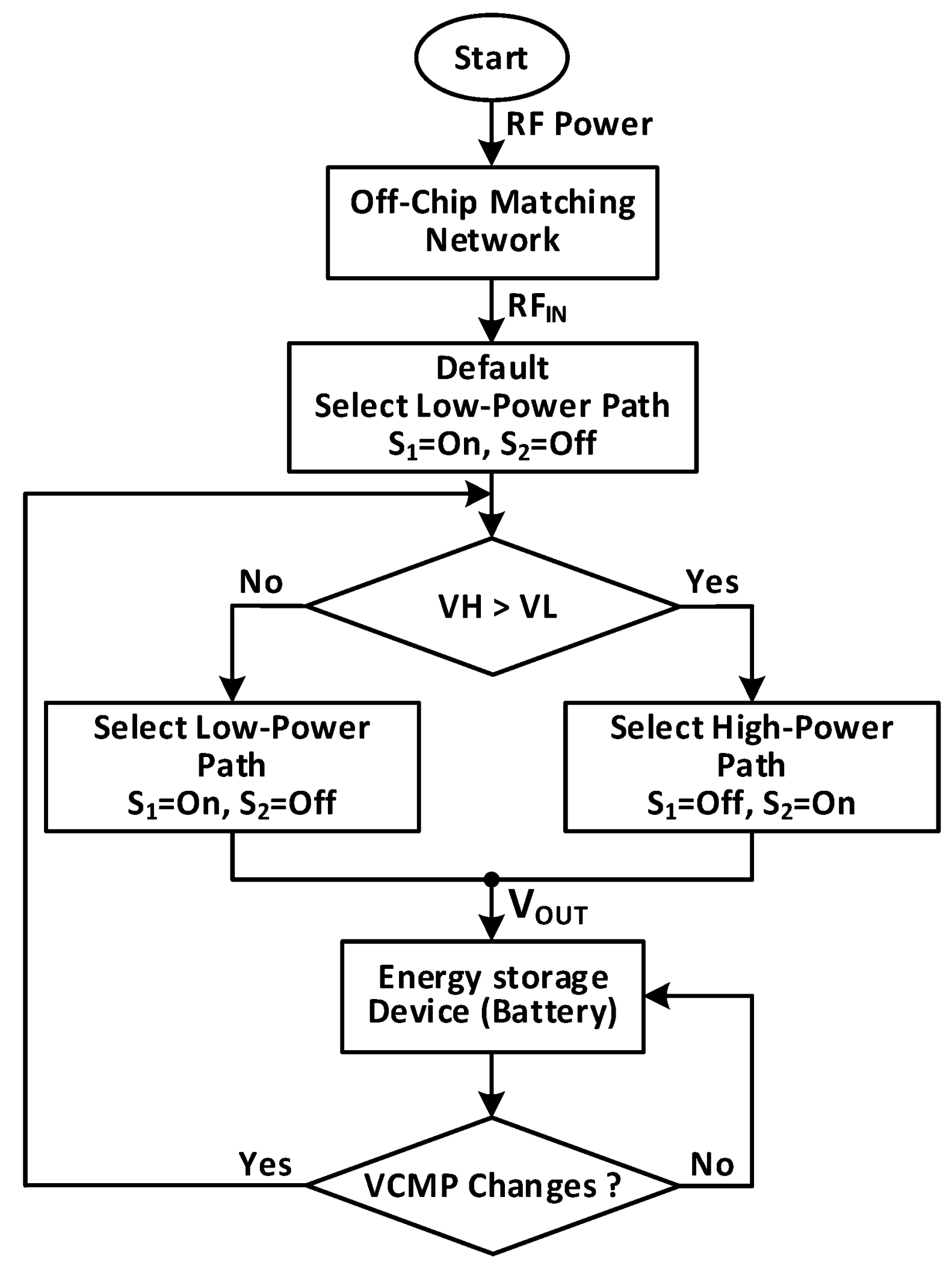
2. Proposed Reconfigurable RF-DC Converter

Figure 2 illustrates the basic concept applied in this proposed circuit. Figure 2a depicts PCE graph of a conventional rectifier that is designed to efficiently work at low-power level. The rectifier achieves high PCE over narrow input power level and its PCE starts to decrease with further increase in input power. On the other hand, Figure 2b shows PCE graph of high-power rectifier which obtains high PCE over narrow high-power range. Figure 2c displays PCE of a reconfigurable rectifier. The reconfigurable rectifier is actually a combination of the low-power rectifier and the high-power rectifier which maintains high PCE over wide input power range. In the reconfigurable rectifier, an adaptive path control (APC) circuit is required to automatically select the low-power rectifier or the high-power rectifier based-on the input power level.
Figure 3 shows the block diagram of the proposed RF-DC converter. A dual path scheme is implemented in the proposed circuit i.e., a low-power path and a high-power path. The low-power path rectifier and the high-power path rectifier are composed of low-threshold voltage (LVT) transistors and high-threshold-voltage (HVT) transistors, respectively. The low-power path rectifier exhibits low input impedance than the high-power path rectifier, courtesy LVT transistors, and harvests more power at low input power level. On the other hand, when input power is increased, the high-power path rectifier harvests more power courtesy HVT transistors. This will be explained in the next section that how LVT and HVT transistors harvest more power at low power and high power, respectively. Each path uses the same rectifier structure but with different transistors in nature. An adaptive path control (APC) circuit is used for the automatic path selection between the two paths based on the input power levels. The APC circuit is composed of a hysteresis common-gate comparator, two PMOS switches (S1 and S2), and an inverter. The comparator compares the outputs of the two paths and activates the switches S1 or S2 based on the input power level.
Figure 4 illustrates the working operation of the proposed circuit. Figure 4a depicts the operation of the low-power path rectifier. At low input power level, the low-power path rectifier harvests more power and produces relatively high voltage (VL) as compared to the output voltage (VH) of the high-power path rectifier. The comparator compares VL and VH and produces low output voltage (VCMP = L) while the inverter produces high output voltage (H). This process makes the switch S1 conductive while the switch S2 non-conductive and activates the low-power path operation. Therefore, as long as VL is higher than the VH, the low-power path rectifier harvests power and delivers to the load that eventually increases the PCE of the low-power path rectifier. Figure 4b shows the working operation of the high-power path rectifier. At high input power conditions, the high-power path rectifier harvests more power than the low-power path rectifier and VH becomes higher than the VL. This makes output voltage of comparator high (VCMP = H) while output of the inverter low (L). This mechanism turns-on and turns-off the switches S2 and S1, respectively, and activates the high-power path. As long as VH is higher than the VL, the high-power path rectifier harvests power and delivers to the load that eventually improves the PCE of the high-power path rectifier. In this way, the overall performance of the proposed circuit increases and a high PCE can be maintained over extended input power range. Figure 5 shows the flowchart of the proposed reconfigurable RF-DC converter.

3. Circuit Description

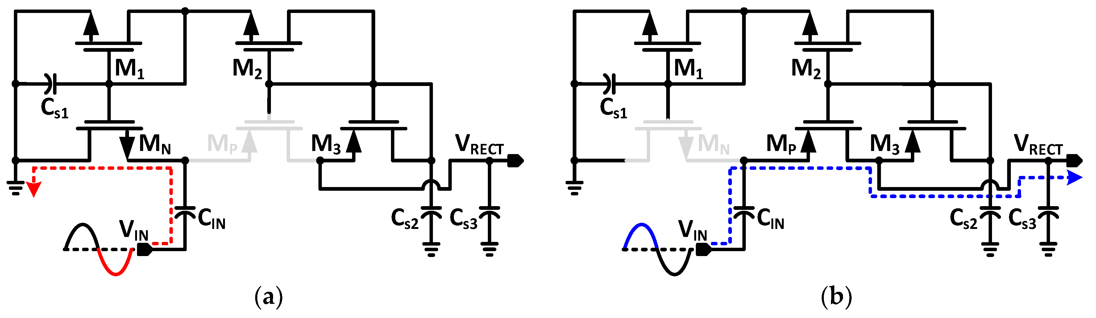
3.1. Rectifier Design

Figure 6 shows the circuit diagram of the rectifier used for both low-power path and high-power path with different transistors in nature. The low-power path rectifier utilizes low-threshold voltage (LVT) transistors to achieve high PCE and better sensitivity at low input power because LVT transistors have thin gate-oxide and require low voltage at their gate terminal to turn-on. Also, leakage current is not increased through LVT transistors when they are reverse biased. However, LVT transistors do not efficiently operate at high input power as leakage current significantly affects their performance when they are reverse biased. Moreover, there is a chance of breakdown of LVT transistors when high voltage is applied at their gate terminal. On contrary, the high-power path rectifier utilizes high-threshold voltage (HVT) transistors for better PCE at high input power. The HVT transistors have thick gate-oxide and require high voltage at their gate terminal to turn-on. At low input power level, the high-power path rectifier is disabled as it exhibits high input impedance due to HVT transistors. The main rectification body of the proposed rectifier is formed by using one NMOS transistor (MN) and one PMOS transistor (MP). The auxiliary transistors M1, M2, and M3 operating in sub-threshold region are used to provide optimum gate-source compensation voltage to the transistors MN and MP of the main rectification chain. In low-power path rectifier, widths of MN and MP are chosen 8 µm and 16 µm, respectively, while their channel length is set to be minimum. The sizes (W/L) of the auxiliary transistors M1, M2, and M3 are selected to be (1 µm/8 µm), (1 µm/4 µm), and (1 µm/2 µm), respectively. The value of the coupling capacitor CIN and the storage capacitors (Cs1 and Cs2) are set to be 400 fF and 1 pF, respectively. In high-power path rectifier, widths of MN and MP are selected to be 20 µm and 40 µm, respectively, while their channel length is set to be minimum (i.e., 600 nm). The sizes of M1, M2, and M3 are chosen (2 µm/12 µm), (2 µm/6 µm), and (2 µm/3 µm), respectively. The value of CIN and the storage capacitors (Cs1 and Cs2) are selected to be 500 fF and 2 pF, respectively.
Consider a single auxiliary transistor MA operating in the sub-threshold region as shown in Figure 6b. A high impedance ZL is placed to limit its drain-source current to the ground. This makes the MA to operate in the sub-threshold region. The leakage current flowing through MA can be written as [32]:
I D , s u b = μ C o x W L ( m 1 ) ( k T q ) 2 e V G S V t h m k T / q ( 1 e V D S k T / q )
where VGS = VDS.
The leakage current ID,sub can be restricted by the high impedance path to the ground while optimum gate-source compensation voltage can be produced by proper sizing (W/L) of the MA. The high impedance path can be created by stacking of diode-connected transistors such as M1, M2, and M3 as shown in Figure 6a. These auxiliary transistors provide compensation voltage to the gates of MN and MP from the drain voltage of the MP. In the proposed rectifier design, gate terminal of the MN is connected to the M1 (a higher voltage with respect to drain of MN) to obtain optimum compensation voltage. This increases overdrive voltage of the MN and minimizes the conduction loss. The overdrive voltage of the MP is increased by connecting its gate terminal to M2 and M3 making its gate voltage lower than its drain voltage. This reduces ON resistance of the MP to have low conduction loss and increases harvested power at the output. The proper sizing of the auxiliary transistors are very important to achieve desired compensation voltage at the gates of MN and MP.
Figure 7 shows the working principle of the proposed rectifier. During charging phase (Figure 7a), the transistor MP enters into non-conducting mode and charging of the coupling capacitor (CIN) starts. By applying Kirchhoff’s voltage law in charging phase, the voltage appeared across CIN is:
V C I N = V I N + V d n
where VIN is the peak amplitude of the RF input voltage, and Vdn is the voltage drop across MN because of threshold voltage. If CIN is considered an ideal capacitor, then whole charge will be delivered to Cs3 during discharging phase without any loss. By applying Kirchhoff’s voltage law during discharging phase (Figure 7b), the voltage developed across Cs3 is given by:
V R E C T = V I N V C I N V d p
By substituting (2) into (3), VRECT can be written as:
V R E C T = 2 V I N V d n V d p
where Vdp is the voltage drop due to threshold voltage across MP. From (4), it is clear that threshold voltages of MN and MP are the dominant factors in the reduction of output voltage (VRECT) of the rectifier. Therefore, proper sizing of the auxiliary transistors compensate the threshold voltages of MN and MP and enhances the performance of the rectifier.

3.2. Adaptive Path Control Circuit Design

As the power harvested from the ambient environment is limited, designing a low-power adaptive path control (APC) circuit is one of the major issues. The APC circuit is composed of a common-gate comparator, two PMOS switches (S1 and S2), and an inverter. Since the switches introduce power loss due to their series resistance, large and optimum sizes of the switches are set to be chosen for low series resistance to exhibit minimum conduction loss. The comparator, being the main part, is shown in Figure 8. Circuit configuration of the proposed comparator is similar to the comparator used in [25]. The comparator is made up of LVT transistors and HVT transistors. The reason of using different threshold voltage transistors is to generate an offset voltage so that dual path is appropriately selected by the comparator. The comparator takes current from outputs of both low-power path rectifier and the high-power path rectifier. At low input supply conditions, the comparator operates in sub-threshold region and its current consumption with respect to VL exhibits exponential growth which is almost negligible. Furthermore, HVT transistors with low current conduction capability decrease the power consumption of the comparator. Even at high input power level, the current consumption of the comparator is less than 1 µA resulting only 1.8% of the output current of the RF-DC converter.

4. Measurement Results

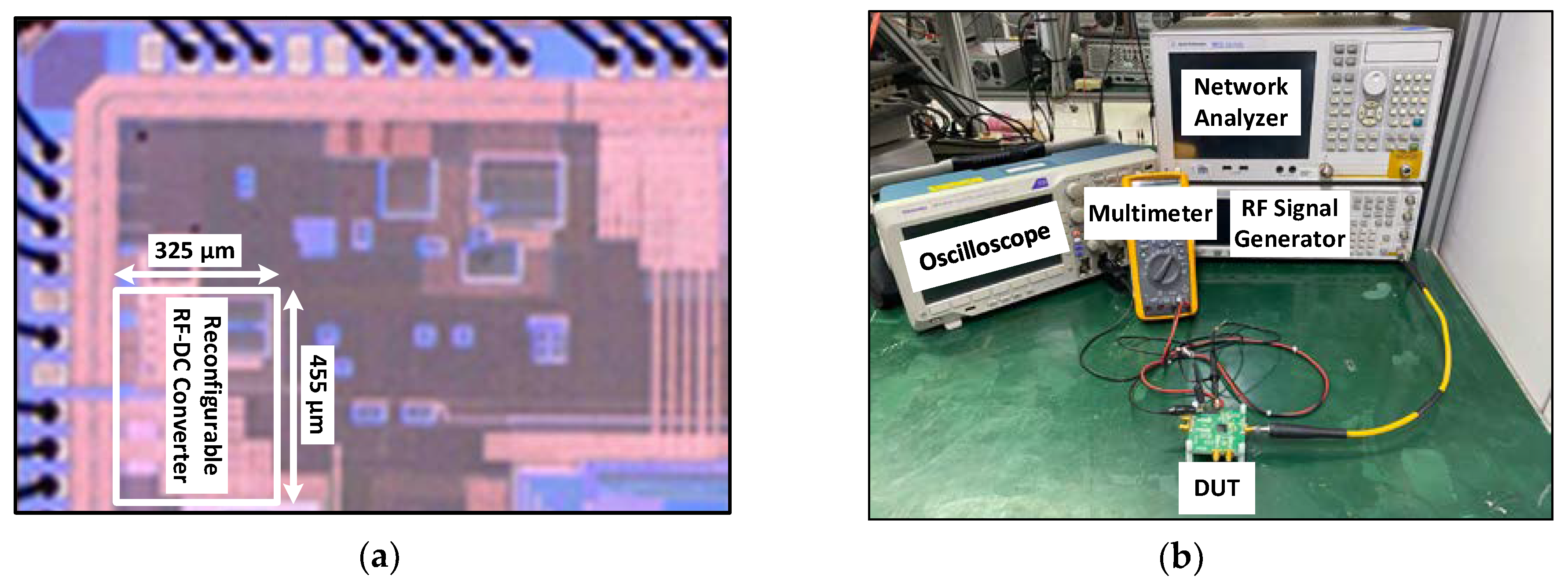
4.1. Microphotograph and Measurement Environment

The proposed circuit is fabricated in 180 nm CMOS technology. The microphotograph of the fabricated chip is shown in Figure 9a. The fabricated chip occupies 325 µm × 455 µm (active area), excluding the pads. The chip is packaged and soldered onto a FR–4 PCB board. Figure 9b shows the measurement setup and the chip is tested with a single-tone sinusoidal signal of 2.45 GHz generated by the signal generator (Agilent E4438C). The output DC voltage is calculated by a digital multimeter and an oscilloscope. An off-chip impedance matching circuit has been implemented between the fabricated chip and the 50-Ω signal generator. The impedance matching circuit boosts incoming sinusoidal voltage and sends to the chip. There are many factors that affect the overall performance of the converter. For instance, the PCB traces losses, reflection losses between the RF-DC converter and impedance matching circuit, and impedance matching circuit losses caused by passive elements. After excluding these losses, net input power is calculated that is given to the chip. The PCE of the proposed RF-DC converter can be calculated using following the equation [33].
η = P o u t P i n = V 2 O U T R L × P i n × 100 %
where Pin is the net input power given to converter, RL is the resistive load, and VOUT is the output voltage.

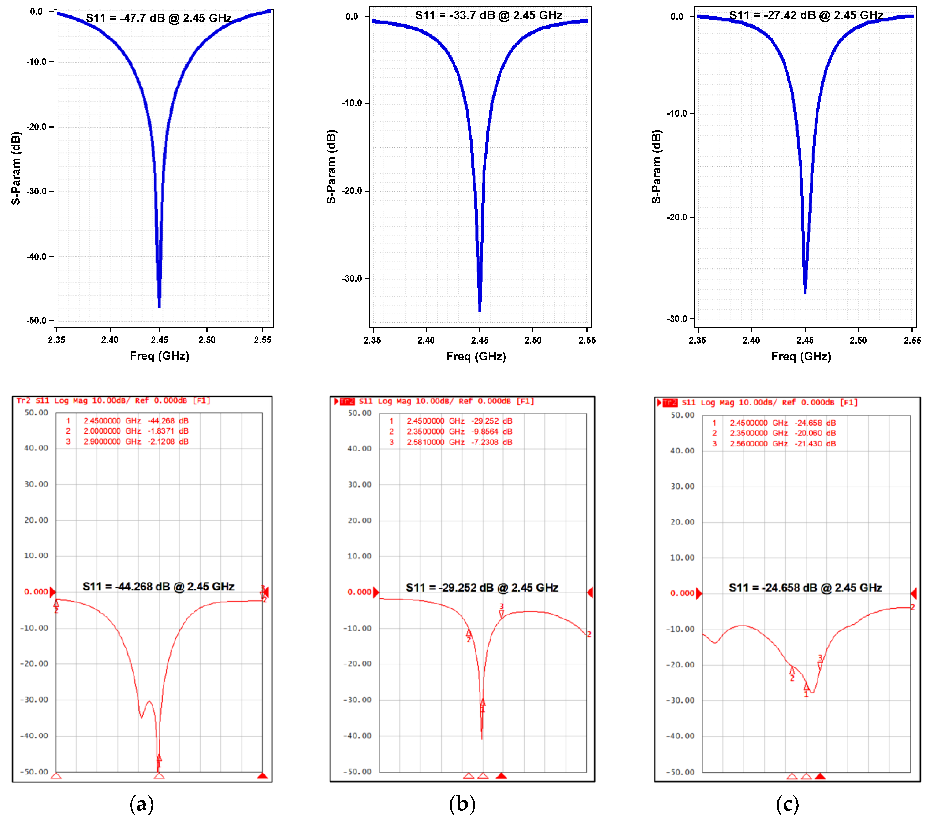
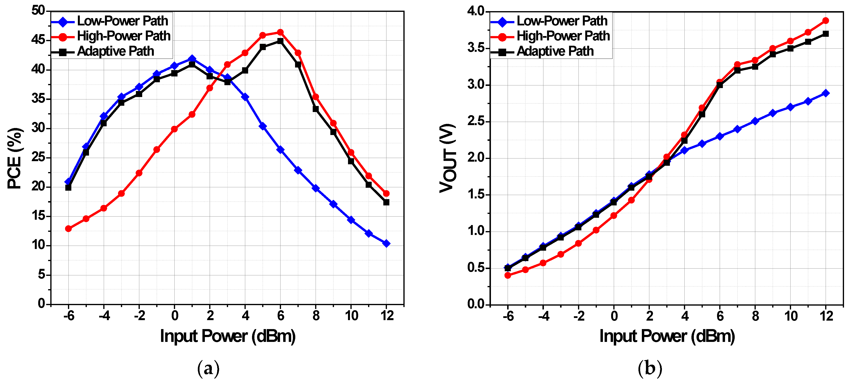
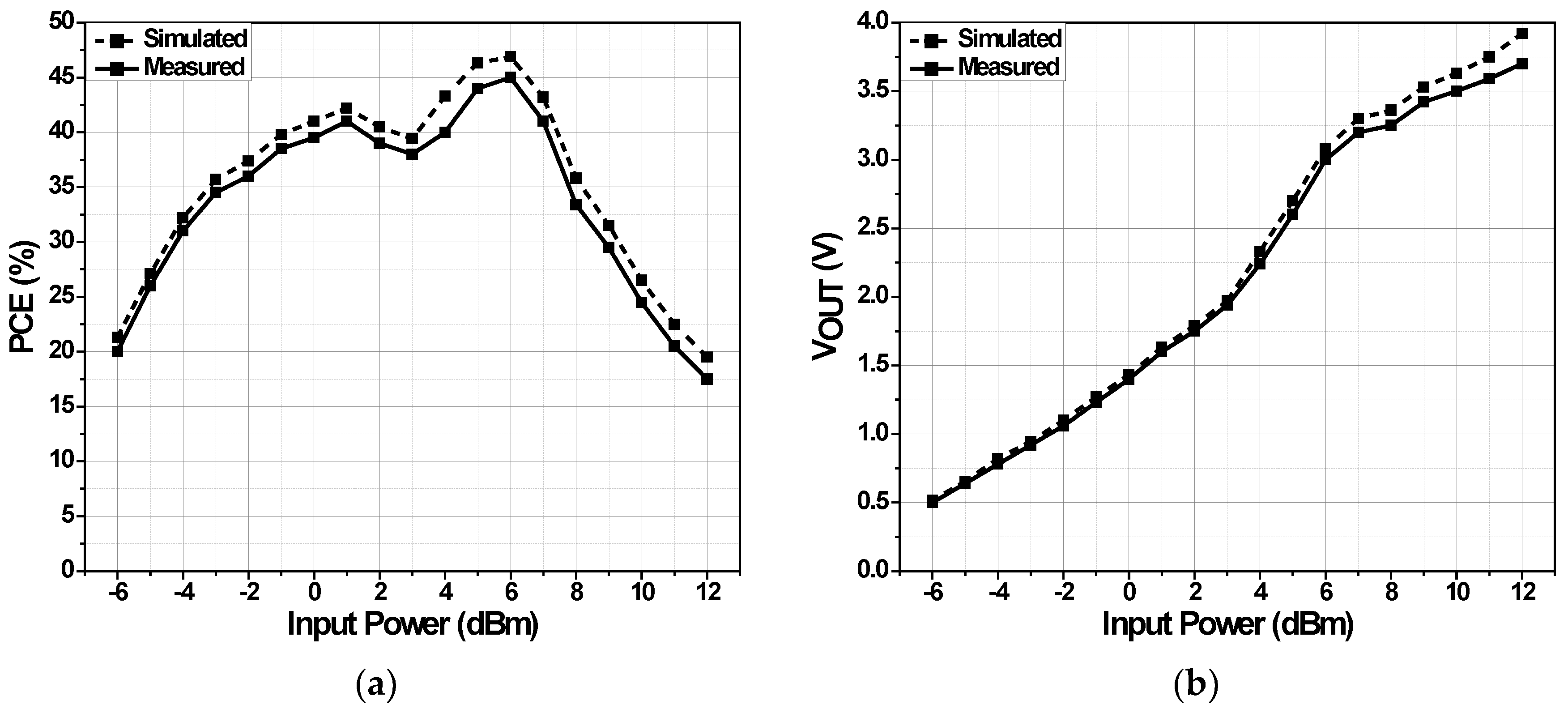
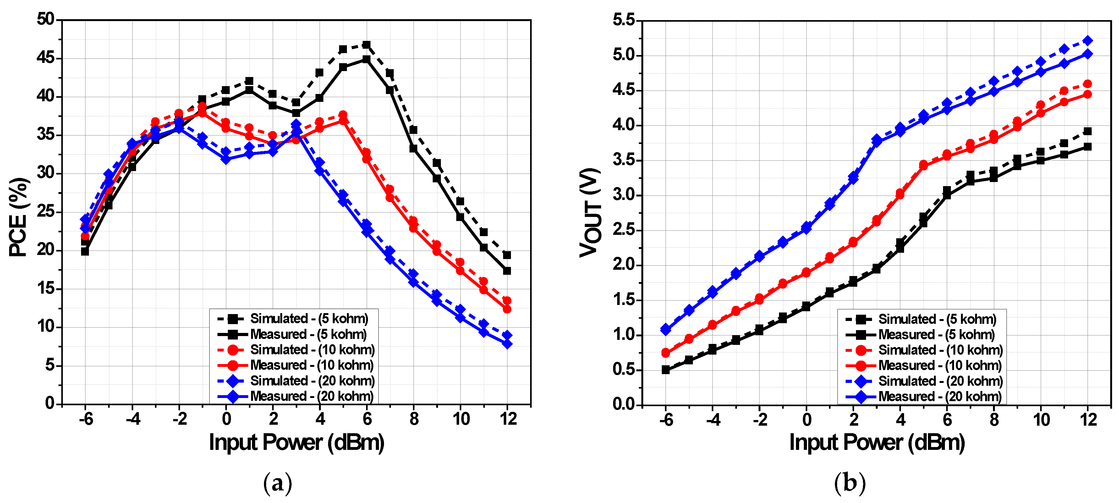
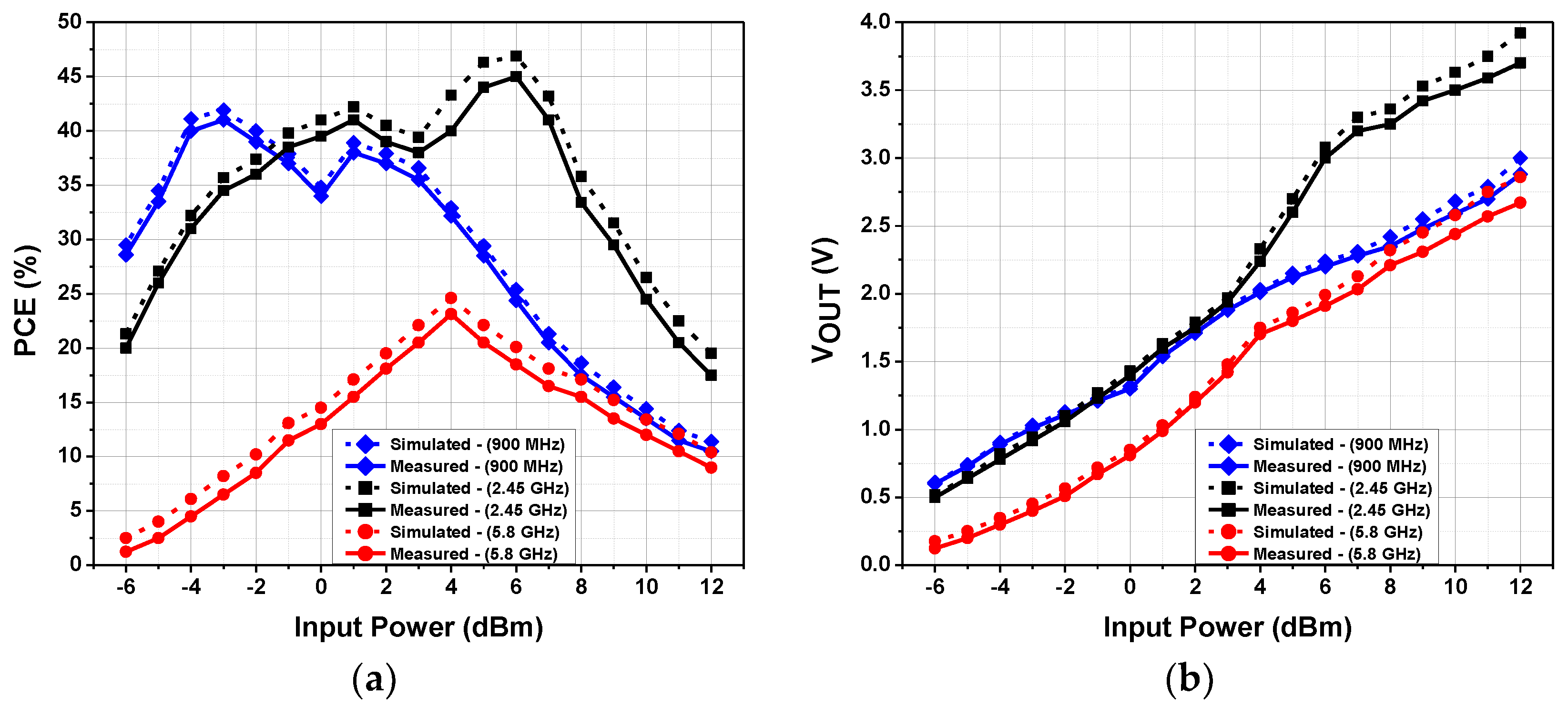
4.2. Performance Measurement

Figure 10 shows the input reflection co-efficient, | S 11 | , for the RF-DC converter. The measured value of | S 11 | at 2.45 GHz is −44.268 dB at 5 kΩ load resistance, which shows the excellent matching. Figure 11 shows simulated and measured value of | S 11 | at different load resistances. Figure 11a–c shows simulated | S 11 | values of (−47.7 dB, −33.7 dB, and −27.42 dB) and measured | S 11 | values of (−44.268 dB, −29.252 dB, and −24.658 dB) at load resistances of 5 kΩ, 10 kΩ, and 20 kΩ, respectively.
The performance of the RF-DC converter is measured by its PCE and output DC voltage. The performance of the low-power path rectifier and the high-power path rectifier are checked separately by using two off-chip control pins namely LP_ENB and HP_ENB. When LP_ENB is high and HP_ENB is low, the low-power path is enabled, whereas when LP_ENB is low and HP_ENB is high, the high-power path is enabled. When both LP_ENB and HP_ENB are connected to high voltage, the proposed circuit operates in the adaptive path selection mode.
Figure 12a shows measured PCE of the proposed circuit as a function of input power for 5 kΩ load resistance. Measurement results show that low-power path rectifier achieves high PCE than the high-power path rectifier from −6 dBm to 2 dBm input power range with peak PCE of 42% at 1 dBm, courtesy LVT transistors. However, PCE of the low-power path rectifier starts decreasing with further increase in the input power. Similarly, high-power path rectifier initially has low PCE at low input power but its PCE starts increasing with the increase in the input power. The high-power path rectifier obtains high PCE than the low-power path rectifier from 3 dBm to 12 dBm input power range with peak PCE of 46.5% at 6 dBm. The adaptive path control (APC) circuit senses the output voltages (VH and VL) of the two paths and automatically switches the circuit between the two paths. In this way, the proposed dual-path RF-DC converter maintains high PCE over extended input power range with peak efficiencies of 41% and 45% at 1 dBm and 6 dBm input powers, respectively. Figure 12b depicts measured output DC voltage of the proposed circuit as a function of input power for 5 kΩ load. The low-power path rectifier has high output DC voltage than the high-power path rectifier from −6 dBm to 2 dBm input power range. From 3 dBm onward, high-power path rectifier has high output DC voltage than the low-power path rectifier. Figure 13 shows the simulated and measured PCE and output DC voltage of the proposed circuit for 5 kΩ load. The measured results reduced a little compared to the simulation results due to parasitic effects and manual welding process.
Figure 14a displays simulated and measured PCE of the proposed circuit as a function of input power for different load conditions. The proposed circuit exhibits maximum simulated efficiencies of (42.2% and 46.9%) and measured efficiencies of (41% and 45%) at input powers of (1 dBm and 6 dBm) for 5 kΩ load resistance. For 10 kΩ load resistance, the proposed circuit achieves maximum simulated efficiencies of (38.9% and 37.8%) and measured efficiencies of (38% and 37%) at input powers of (−1 dBm and 5 dBm). Similarly, maximum simulated efficiencies of (36.9% and 36.6%) and measured efficiencies of (36% and 35.5%) are obtained at input powers of (−2 dBm and 3 dBm) across 20 kΩ load resistance. As the load resistance increases, the PCE curve shifts to the left side. Figure 14b shows simulated and measured output DC voltage as a function of input power for different loads. It can be seen that the output DC voltage of the proposed circuit increases by increasing the load resistance.
Figure 15a presents simulated and measured PCE of the proposed circuit at different frequencies for 5 kΩ load. The proposed circuit displays superior PCE at 2.45 GHz (as it is designed and optimized for 2.45 GHz) compared to other frequencies of 900 MHz and 5.8 GHz. At 900 MHz, the proposed circuit achieves maximum simulated efficiencies of (41.9% and 38.9%) and measured efficiencies of (41% and 38%) at input powers of (−3 dBm and 1 dBm). While at 5.8 GHz, the maximum simulated and measured efficiencies of 24.6% and 23.12%, respectively, are obtained at 4 dBm input power. Figure 15b shows simulated and measured output DC voltage at different frequencies across 5 kΩ load.

4.3. Comparison with Published Works

Table 1 provides a summary of performance parameters of the proposed circuit and compares it with recent published works. The proposed circuit, despite being a single-ended structure and not depending on a PCB balun, demonstrates relatively better performance than the reported works. Courtesy to dual-path adaptive structure, the proposed circuit obtains high PCE over wide input power sweep. For 5 kΩ load resistance, the proposed circuit obtains maximum efficiencies of 41% and 45% at 1 and 6 dBm input powers, respectively. Moreover, the proposed circuit maintains more than 20% PCE from −6 to 11 dBm input power range. However, the circuits reported in [33] and [18] obtain higher PCE at higher input power than this work, while the circuit reported in [19] achieves higher PCE at lower input power in comparison to the proposed work at 2.45 GHz frequency.

5. Conclusions

This paper presents a reconfigurable 2.45-GHz RF-DC power converter to efficiently harvest electromagnetic energy over extended input power range. The proposed circuit consists of a dual-path i.e., a low-power path and a high-power path, and an adaptive path control circuit. The adaptive path control circuit switches the converter between the low-power path and the high-power path to transfer the harvested power to the output based on the input power level. The proposed structure has been designed and implemented in a 180-nm CMOS technology. The measured PCE is above 20% ranging from −6 to 11 dBm with maximum efficiencies of 41% and 45% at 1 and 6 dBm input powers, respectively, for 5 kΩ resistive load. Moreover, the proposed circuit performs well at 900 MHz and 5.8 GHz frequencies.

Author Contributions

Conceptualization, D.K. and M.B.; methodology, D.K.; software, D.K., K.S., and Q.U.A.; validation, D.K., D.V., M.A., and S.J.O.; formal analysis, D.K., M.B., and K.S.; investigation, D.K. and M.B.; resources, D.K.; data curation, D.K. and M.B.; writing—original draft preparation, D.K. and K.-Y.L.; writing—review and editing, D.K., M.B., Y.G.P., S.-S.Y., and K-Y.L.; visualization, D.K., M.B., and K.-Y.L.; supervision, K.C.H., Y.Y., and K.-Y.L.; project administration, K-Y.L. All authors have read and agreed to the published version of the manuscript.

Funding

This work was supported by the National Research Foundation of Korea (NRF) grant funded by the Korea government (MSIP) (2014R1A5A1011478).

Conflicts of Interest

The authors declare no conflict of interest.

References

  1. Jonah, O.; Georgakopoulos, S.V. Wireless power transfer in concrete via strongly coupled magnetic resonance. J. Chem. Inf. Model. 2013, 53, 1689–1699. [Google Scholar] [CrossRef]
  2. Hekal, S.; Abdel-Rahman, A.B.; Jia, H.; Allam, A.; Barakat, A.; Pokharel, R.K. A novel technique for compact size wireless power transfer applications using defected ground structures. IEEE Trans. Microw. Theory Tech. 2017, 65, 591–599. [Google Scholar] [CrossRef]
  3. Yedavalli, P.S.; Riihonen, T.; Wnag, X.; Rabaey, J.M. Far-field RF wireless power transfer with blind adaptive beamforming for Internet of Things devices. IEEE Access 2017, 5, 1743–1752. [Google Scholar] [CrossRef]
  4. Xia, M.; Aissa, S. On the efficiency of far-field wireless power transfer. IEEE Trans. Signal Process. 2015, 63, 2835–2847. [Google Scholar] [CrossRef] [Green Version]
  5. Xiao, L.; Wang, P.; Niyato, D.; Kim, D.; Han, Z. Wireless networks with RF energy harvesting: A contemporary survey. IEEE Commun. Surv. Tuts 2015, 17, 757–789. [Google Scholar]
  6. Lu, Y.; Law, M.-K.; Sin, S.-W.; Seng-Pan, U.; Martins, R.P. A review and design of the on-chip rectifiers for RF energy harvesting. In Proceedings of the IEEE International Wireless Symposium, Shenzhen, China, 30 March–1 April 2015. [Google Scholar]
  7. Harouni, Z.; Cirio, L.; Osman, L.; Gharsallah, A.; Picon, O. A dual circularly polarized 2.45-GHz rectenna for wireless power transmission. IEEE Antennas Wirel. Propag. Lett. 2011, 10, 306–309. [Google Scholar] [CrossRef]
  8. Bito, J.; Hester, J.G.; Tentzeris, M.M. Ambient RF energy harvesting from a two-way talk radio for flexible wearable wireless sensor devices utilizing inkjet printing technologies. IEEE Trans. Microw. Theory Tech. 2015, 63, 4533–4543. [Google Scholar] [CrossRef]
  9. Abouzied, M.A.; Sanchez-Sinencio, E. Low-input power-level CMOS RF energy-harvesting front end. IEEE Trans. Microw. Theory Tech. 2015, 63, 3794–3805. [Google Scholar] [CrossRef]
  10. Ren, Y.-J.; Chang, K. 5.8-GHz circularly polarized dual-diode rectenna and rectenna array for microwave power transmission. IEEE Trans. Microw. Theory Tech. 2006, 54, 1495–1502. [Google Scholar]
  11. Kuhn, V.; Lahuec, C.; Seguin, F.; Person, C. A multi-band stacked RF energy harvester with RF-to-DC efficiency up to 84%. IEEE Trans. Microw. Theory Tech. 2015, 63, 1768–1778. [Google Scholar] [CrossRef]
  12. Abouzied, M.A.; Ravichandran, K.; Sánchez-Sinencio, E. A fully integrated reconfigurable self-startup RF energy harvesting system with storage capability. IEEE J. Solid-State Circuits 2017, 52, 704–719. [Google Scholar] [CrossRef]
  13. Curty, J.-P.; Joehl, N.; Krummenacher, F.; Dehollian, C.; Declercq, M.J. A model for μ-power rectifier analysis and design. IEEE Trans. Circuits Syst. I Reg. Pap. 2005, 52, 2771–2779. [Google Scholar] [CrossRef]
  14. FCC Codes of Regulation, Part 15 [Online]. Available online: http://www.access.gpo.gov/nara/cfr/waisidx_03/ (accessed on 20 April 2020).
  15. Hameed, Z.; Moez, K. A 3.2 V—15 dBm adaptive threshold-voltage compensated RF energy harvester in 130 nm CMOS. IEEE Trans. Circuits Syst. I Reg. Pap. 2015, 62, 948–956. [Google Scholar] [CrossRef]
  16. Li, C.-J.; Lee, T.-C. 2.4-GHz high-efficiency adaptive power. IEEE Trans. Very Large Scale Integr. (VLSI) Syst. 2014, 22, 434–438. [Google Scholar] [CrossRef]
  17. Dehghani, S.; Johnson, T. A 2.4-GHz CMOS class-E synchronous rectifier. IEEE Trans. Microw. Theory Tech. 2016, 64, 1655–1666. [Google Scholar] [CrossRef]
  18. Fan, S.; Yuan, H.; Gou, W.; Zhao, Y.; Song, C.; Huang, Y.; Zhou, J. A 2.45 GHz rectifier-booster regulator with impedance matching converters for wireless energy harvesting. IEEE Trans. Microw. Theory Tech. 2019, 67, 3833–3843. [Google Scholar] [CrossRef]
  19. Xu, P.; Flandre, D.; Bol, D. Analysis, modeling, and design of a 2.45-GHz RF energy harvester for SWIPT IoT smart sensors. IEEE J. Solid-State Circuits 2019, 54, 2717–2729. [Google Scholar] [CrossRef]
  20. Kim, S.-Y.; Abbasizadeh, H.; Rikan, B.S.; Oh, S.J.; Jang, B.G.; Park, Y.-J. A −20 to 30 dBm input power range wireless power system with a MPPT-based reconfigurable 48% efficient RF energy harvester and 82% efficient A4WP wireless power receiver with open loop delay compensation. IEEE Trans. Power Electron. 2018, 34, 6803–6817. [Google Scholar] [CrossRef]
  21. Khan, D.; Abbasizadeh, H.; Kim, S.-Y.; Khan, Z.H.N.; Shah, S.A.A.; Pu, Y.G.; Hwang, K.C.; Yang, Y.; Lee, M.; Lee, K.-Y.; et al. A design of ambient RF energy harvester with sensitivity of -21dBm and power efficiency of a 39.3% using internal threshold voltage compensation. Energies 2018, 11, 1258. [Google Scholar] [CrossRef] [Green Version]
  22. Khan, D.; Oh, S.J.; Shehzad, K.; Verma, D.; Khan, Z.H.N.; Pu, Y.G. A CMOS RF energy harvester with 47% peak efficiency using internal threshold voltage compensation. IEEE Micow. Wirel. Compon. Lett. 2019, 29, 415–417. [Google Scholar] [CrossRef]
  23. Saffari, P.; Basaligheh, A.; Moez, K. An RF-to-DC recifier with high efficiency over wide input power range for RF energy harvesting applications. IEEE Trans. Circuits Syst. I Reg. Pap. 2019, 66, 4862–4875. [Google Scholar] [CrossRef]
  24. Li, B.; Shao, X.; Shahshahan, N.; Goldsman, N.; Salter, T.; Metze, G. An antenna co-design dual band RF energy harvester. IEEE Trans. Circuits Syst. I Reg. Pap. 2013, 60, 3256–3266. [Google Scholar] [CrossRef]
  25. Lu, Y.; Dai, H.; Huang, M.; Law, M.-K.; Sin, S.-W.; Seng-Pan, U.; Martins, R.P. A wide input range dual-path CMOS rectifier for RF energy harvesting. IEEE Trans. Circuits Syst. II Exp. Briefs. 2017, 64, 166–170. [Google Scholar] [CrossRef]
  26. Papotto, G.; Carrara, F.; Palmisano, G. A 90-nm CMOS threshold- compensated RF energy harvester. IEEE J. Solid-State Circuits 2011, 46, 1985–1997. [Google Scholar] [CrossRef]
  27. Stoopman, M.; Keyrouz, S.; Visser, H.J.; Philips, K.; Serdijn, W. Co-design of a CMOS rectifier and small loop antenna for highly sensitive RF energy harvesters. IEEE J. Solid-State Circuits 2014, 49, 622–634. [Google Scholar] [CrossRef]
  28. Scorcioni, S.; Larcher, L.; Bertacchini, A. A reconfigurable differential CMOS RF energy scavenger with 60% peak efficiency and -21 dBm sensitivity. IEEE Microw. Wirel. Compon. Lett. 2013, 23, 155–157. [Google Scholar] [CrossRef]
  29. Mansour, M.M.; Ichihashi, M.; Kanaya, H. Wide-band and efficiency-improved 0.18um CMOS RF differential rectifier for wireless energy harvesting. In Proceedings of the 2019 IEEE Asia-Pacific Microwave Conference (APMC), Singapore, 10–13 December 2019; pp. 141–143. [Google Scholar]
  30. Lee, D.; Kim, T.; Kim, S.; Byun, K.; Kwon, K. A CMOS rectifier with 72.3% RF-to-DC conversion efficiency employing tunable impedance matching network for ambient RF energy harvesting. In Proceedings of the 2018 International SoC Design Conference (ISOCC), Daegu, Korea, 12–15 November 2018; pp. 259–260. [Google Scholar]
  31. Li, X.; Huang, M.; Martins, R.P. A 2.4-GHz mid-field CMOS wireless power receiver achieving 46% maximum PCE and 163-mW output power. IEEE Trans. Circuits Syst. II 2020, 67, 360–364. [Google Scholar] [CrossRef]
  32. Taur, Y.; Ning, T.H. Fundamentals of Modern VLSI Devices; Cambridge University Press: Cambridge, UK, 1998. [Google Scholar]
  33. Khan, D.; Oh, S.J.; Shehzad, K.; Basim, M.; Verma, D.; Pu, Y.G.; Lee, M.; Hwang, K.C. An efficient reconfigurable RF-DC converter with wide input power range for RF energy harvesting. IEEE Access 2020, 8, 79310–79318. [Google Scholar] [CrossRef]
Figure 1. Block diagram of an Radio Frequency (RF) energy harvesting system.
Electronics 09 01107 g001
Figure 2. Conventional rectifier’s efficiencies: (a) at low-power; (b) at high-power; and (c) proposed reconfigurable rectifier’s efficiency.
Electronics 09 01107 g002
Figure 3. Block diagram of the proposed RF-DC converter.
Electronics 09 01107 g003
Figure 4. Proposed RF-DC converter with (a) operation of low-power path rectifier; and (b) operation of high-power path rectifier.
Electronics 09 01107 g004
Figure 5. Flowchart of the proposed reconfigurable RF-DC converter.
Electronics 09 01107 g005
Figure 6. (a) Circuit diagram of the proposed rectifier. (b) Auxiliary transistor for producing optimum compensation voltage.
Electronics 09 01107 g006
Figure 7. Working principle of the proposed rectifier. (a) Charging phase; and (b) discharging phase.
Electronics 09 01107 g007
Figure 8. Schematic of the common-gate comparator.
Electronics 09 01107 g008
Figure 9. (a) Chip microphotograph, (b) Measurement setup to test the chip.
Electronics 09 01107 g009
Figure 10. Measured input reflection co-efficient, | S 11 | , for RF-DC converter at 5 kΩ load.
Electronics 09 01107 g010
Figure 11. Simulated and measured | S 11 | for RF-DC converter at (a) 5 kΩ; (b) 10 kΩ; and (c) 20 kΩ load.
Electronics 09 01107 g011
Figure 12. Measured results of the proposed circuit for 5 kΩ load. (a) PCE; and (b) output DC voltage.
Electronics 09 01107 g012
Figure 13. Simulated and measured results of the proposed circuit for 5 kΩ load. (a) PCE; and (b) output DC voltage.
Electronics 09 01107 g013
Figure 14. Simulated and measured results of the proposed circuit for different loads. (a) PCE; and (b) output DC voltage.
Electronics 09 01107 g014
Figure 15. Simulated and measured results of the proposed circuit at different frequencies. (a) PCE; and (b) output DC voltage.
Electronics 09 01107 g015
Table 1. Performance summary.
This WorkTCAS-II-20 [33]TMTT-16 [17]TMTT-19 [18]JSSC-19 [19]TPE-18 [20]ISOCC-18 [30]
Technology180 nm28 nm130 nmDiode-Based65 nm180 nm130 nm
Frequency2.45 GHz2.40 GHz2.40 GHz2.45 GHz2.45 GHz0.90 GHz0.7–0.9
TopologySECCClass ERBRCCSECC
TechniqueDual-path---MPPTMPPTT-MN
Peak PCE and at different input power levelsPeak: 45%
@ 6 dBm
Peak: 46%
@ 25.5 dBm *
Peak: 30%
@ 10 dBm
Peak: 37.5%
@ 13 dBm
Peak: 48.3%
@ −3 dBm
Peak: 48.2%
@ 0 dBm
Peak: 72.3%
@ −15 dBm
20%
@ −6 dBm
20%
@ 18 dBm *
10%
@ 0 dBm *
17.5%
@ 0 dBm *
25%
@ −10 dBm *
31.8%
@ −20 dBm
40%
@ −18 dBm *
20.5%
@ 11 dBm
35%
@ 30 dBm *
21%
@ 18 dBm *
35%
@ 15 dBm *
46%
@ 0 dBm
41.1%
@ 20 dBm
20%
@ −5 dBm *
Load5 kΩ24 Ω-20 kΩPMU23 kΩ10 kΩ
SE: single-ended, CC: cross-coupled, RBR: rectifier booster regulator, T-MN: tunable matching network, * Estimated from graph.

