Article

Polarization-Charge Inversion at Al2O3/GaN Interfaces through Post-Deposition Annealing

1
Department of Electronic and Electrical Convergence Engineering, Hongik University, Sejong 30016, Korea
2
School of Electronics Engineering, Kyungpook National University, Daegu 41566, Korea
*
Authors to whom correspondence should be addressed.
Electronics 2020, 9(7), 1068; https://doi.org/10.3390/electronics9071068
Submission received: 2 June 2020 / Revised: 20 June 2020 / Accepted: 29 June 2020 / Published: 30 June 2020
(This article belongs to the Special Issue Applications of Thin Films in Microelectronics)

Abstract

:
The effects of post-deposition annealing (PDA) on the formation of polarization-charge inversion at ultrathin Al2O3/Ga-polar GaN interfaces are assessed by the analysis of energy band bending and measurement of electrical conduction. The PDA-induced positive interface charges form downward energy band bending at the Al2O3/GaN interfaces with polarization-charge inversion, which is analyzed using X-ray photoelectron spectroscopy. Net charge and interface charge densities at the Al2O3/GaN interfaces are estimated after PDA at 500 °C, 700 °C, and 900 °C. The PDA temperatures affect the formation of charge densities. That is, the charge density increases up to 700 °C and then decreases at 900 °C. Electrical characteristics of GaN Schottky diodes with ultrathin Al2O3 layers exhibit the passivation ability of the Al2O3 surface layer and the effects of polarization-charge inversion through PDA. This result can be applied to improvement in GaN-based electronic devices where surface states and process temperature work important role in device performance.

1. Introduction

Chemical and physical properties at GaN surfaces and interfaces have a remarkable influence on the electronic device performance and stability [1,2,3,4,5]. GaN-based Schottky contact is a prevailing basic building block for power switching components, based on the material’s robust properties such as high breakdown field, direct wide bandgap, radiation hardness, high electron mobility, and high saturation velocity [6,7,8,9,10,11,12,13]. Due to the unavoidable surface and interface trap charges and defect states originated from the dangling bonds and threading dislocations on GaN surface, drawbacks of conduction in GaN electronic components are observed, such as leakage current, current collapse, and premature breakdown [14,15,16,17,18,19,20,21,22,23]. Deposition of a high-k dielectric passivation layer can counteract the effects of surface states on the conduction. Al2O3 is a prevalent dielectric material for surface passivation owing to large bandgap, high permittivity, and high breakdown field [24,25,26,27].
Post-deposition annealing (PDA) is a subsequent step for atomic-layer deposition (ALD) Al2O3 thin film to enhance interface quality and passivation ability. Some researches represent the experimental discovery of energy band bending at high-k dielectric/GaN interfaces with PDA [6,7,8,9,10,24,25,26,27]. Energy band bending at the GaN interfaces is associated with the interface charge density and surface potential formed by PDA. Therefore, the fundamentals of physical and chemical phenomena occurred at the interface through the PDA should be analyzed to understand the conduction in GaN electronic devices with Al2O3 passivation. Up to now, the analysis on the energy band bending and surface potential at the Al2O3/GaN interfaces is mainly of metal-oxide-semiconductor structure in which the thickness of the gate oxide layer is thicker than the thickness of the oxide layer for a surface passivation [3,6,7,8]. The correlation between the PDA-induced surface states and device performance remains unexplored, too, though the verification of the mechanism at the interface is prerequisite for device design and optimization.
In this work, the effects of PDA on the formation of polarization-charge inversion at Al2O3/GaN interfaces are examined through the analysis of energy band bending and measurements of electrical property with PDA at 500 °C, 700 °C and 900 °C. The downward band bending is observed at the Al2O3/GaN interfaces after the PDA at 700 and 900 °C, attributed to the formation of positive interface charges that lead to polarization-charge inversion. The quality of charge carriers’ flow in GaN SDs improved with the positive charges formed by the PDA in addition to passivation ability of Al2O3 surface layers. However, leakage current level increases at the 900 °C PDA due to the micro-crystallization of Al2O3. The principles for the changes in energy band bending at the Al2O3/GaN interfaces and improved conduction in the Al2O3/GaN SDs are discussed.

2. Materials and Methods

Wurtzite Ga-polar GaN was grown by metal organic chemical vapor deposition with a Si doping concentration of 5 × 1017 cm−3 from the top surface to 400 nm depth for a Schottky contact region, and 5 × 1018 cm−3 from 400 to 800 nm depth for an ohmic contact region. As-grown GaN substrates were treated with sulfuric acid peroxide mixture (SPM) and RCA cleaning procedures. The GaN go through a sonicating in acetone and isopropyl alcohol (as-prepared GaN), followed by dipping into a SPM solution (Piranha, H2SO4:H2O2 = 3:1) and an ammonium hydroxide solution (NH4OH:H2O2:DI H2O = 1:1:5) for organic debris removal, then a hydrofluoric acid solution (HF:DI H2O = 1:50) for surface oxide removal, and a hydrochloric acid solution (HCl:H2O2:DI H2O = 1:1:5) for ionic debris removal (as-cleaned GaN). Al2O3 was deposited on the as-cleaned GaN by ALD. The GaN samples were loaded into an ex-situ ALD chamber, where an H2O source was applied as an oxidant at a stage temperature of 250 °C, followed by ten- and thirty-cycles deposition of Al(CH3)3 and H2O precursors in alternative pulses. The growth rate of ALD layer is 1.0 Å/cycle. The Al2O3-deposited GaN then went through PDA in a N2 ambient at 500 °C, 700 °C and 900 °C for 3 min, respectively. For a circular-shaped Schottky diode (SD) fabrication, the ground mesa was first formed by inductively coupled plasma-reactive ion etching (ICP-RIE). After the etching, the samples were cleaned to remove PR residue and induced charges during ICP-RIE process. After an additional pattering for ground metal area which is few micrometers smaller in dimension than that of the pattering for Schottky gate mesa. Then, Ti/Al/Ti/Au (20/180/20/80 nm) stack was deposited, followed by ohmic annealing at 650 °C for 30 s. The gate contact area was defined and then dipped in a diluted HF solution to etch away the Al2O3 layer above the contact area. Ni/Au (20/180 nm) was deposited for a Schottky contact (Figure 1a).
Effects of PDA on the energy band bending at the ultrathin Al2O3/GaN interfaces were assessed by an X-ray photoelectron spectroscopy (XPS) measurement. A monochromatic 1486.60 eV Al Kα X-ray source was applied to scanning with 0.04 eV scan step, 100 µm spot size, 50 eV pass energy, and 50 ms dwell time. The measurement energy scale was calibrated using the Cu 2p3/2, Ag 3d5/2, and Au 4f7/2 standard binding energy peak positions. The C 1s peak was referenced to 284.80 eV to offset charge effect. The survey scans were repeated 10 times. The electrical measurements were performed by semiconductor parameter analyzer system. All measurements were conducted at room temperature.

3. Results and Discussion

XPS is utilized to identify the surface polarity of GaN by scanning a near-valence band (VB) region (Figure 1b). There are two well-defined peaks (P1 and P2) emerged from the atomic p- and s-orbital states of GaN [28,29]. The P1 and P2 peaks at the binding energy (BE) of 4.00 eV and 8.66 eV, individually, are associated with the Ga 4p-N 2p hybridization and Ga 4s-N 2p hybridization states, respectively. Here, the intensity of P1 peak is stronger than that of the P2 peak, with the 1.14 intensity ratio of P1 to P2 peaks, which verifies Ga-face polarity of GaN [28]. The BE difference obtained from the peak shift in Ga 3d core levels can represent the surface band bending of GaN (Figure 1c). The Ga 3d peak BEs of as-prepared and as-cleaned GaN are 19.82 and 19.68 eV, respectively, which indicates a demonstration of 0.14 eV upward band bending on the GaN surface after cleaning steps. An internal spontaneous polarization (Psp = −0.033 C·m−2) of Ga-faced GaN heading from surface to bulk forms negative bound sheet charges (1.81 × 1013 cm−2) nearby the surface band therefore induces upward band bending [8,30,31].
Figure 2 exhibits XPS spectra of Ga 3d, Al 2p, O 1s, and N 1s core levels at 1 nm Al2O3/GaN interfaces with no PDA (sample A1) and with PDA at 500 °C (sample B1), 700 °C (sample C1), and 900 °C (sample D1) for 3 min. The peak BE of Ga 3d core level of 1 nm Al2O3 as-deposited GaN (A1) is located at 19.55 eV and then the peak BE shifts to 19.70, 20.16 and 20.01 eV with the 3 min PDA at 500 °C, 700 °C and 900 °C, individually (Figure 2a). The increase in the peak BE of Ga 3d core levels upon PDA indicates the increase in Ga-O bonding at the Al2O3/GaN interfaces in which O atoms diffuse from Al2O3 to GaN through PDA [32,33]. The behavior of the peak shift in Al 2p core level according to the PDA conditions is similar with that of Ga 3d core level. The peak BE of Al 2p core level at the 1 nm Al2O3/GaN interface is located at 75.60 eV, then shifts to 75.74, 76.22 and 76.11 eV, with the 3 min PDA at 500 °C, 700 °C and 900 °C, respectively (Figure 2b), in which the peak position shifts to higher BE through PDA supports the diffusion of O atoms into GaN.
Figure 3 displays XPS spectra of Ga 3d, Al 2p, O 1s, and N 1s core levels at 3 nm Al2O3/GaN interfaces with no PDA (sample A3) and with PDA at 500 °C (sample B3), 700 °C (sample C3), and 900 °C (sample D3) for 3 min. The peak BEs of Ga 3d are 19.50, 19.64, 20.22 and 20.05 eV (Figure 3a), and the BEs of Al 2p are 75.56, 75.68, 76.30 and 76.16 eV for the samples A3, B3, C3, and D3, respectively (Figure 3b). The increase in the peak BEs of Ga 3d and Al 2p core levels through PDA agree with the outcomes of O diffusion at the 1 nm Al2O3/GaN interfaces. The XPS measurement results are summarized in Table 1.
The energy band bending at the 1 nm Al2O3/GaN interfaces with the PDA conditions are shown in Figure 4a‒d. (‒) 0.27 eV surface potential (Ψs) with an upward band bending is formed on the GaN surface after the deposition of 1 nm Al2O3. The Ψs decreases to (‒) 0.10 eV, 0.34 eV, and increases back to 0.19 eV for the samples A1, B1, C1, and D1. The valence band offset (VBO) at the Al2O3/GaN interfaces are determined by the equation [6,24,25]:
VBO = [ E C L G a N E V G a N ] b [ E C L A l 2 O 3 E V A l 2 O 3 ] b [ E C L G a N E C L A l 2 O 3 ] i
where ECL are the BEs of atomic core levels, EV are the BEs of VBMs, and subscripts b and i stand for the bulk GaN and Al2O3/GaN interface, respectively. The second term for bulk Al2O3 is estimated to be 71.60 eV. The VBO values at the 1 nm Al2O3/GaN interfaces with the different PDA conditions are determined to be 1.94, 1.93, 1.95 and 1.99 eV for the samples A1, B1, C1, and D1, individually. The bandgap (Eg) of Al2O3 is 7.00 eV and conduction band offsets (CBOs) are obtained by mathematical operations.
For the cases of 3 nm Al2O3-deposited GaN, same methodology with the 1 nm Al2O3 cases is applied to the determination of Ψs, VBO, and CBO at the 3 nm Al2O3/GaN interfaces and the verification of the effect of oxide layer thickness on the surface band bending. The energy band bending at the 3 nm Al2O3/GaN interfaces with the PDA conditions are exhibited in Figure 5a‒d.
For both cases of 1 and 3 nm Al2O3 interfaces, the directions of band bending change from upward without and with 500 °C PDA (A1, B1, A3, and B3) to downward with 700 °C and 900 °C PDA (C1, D1, C3 and D3). The surface polarity inversion possibly occurs due to the compensation of internal polarization charges by the ionized donors in space charge region of n-GaN and positive interface charges formed at the Al2O3/GaN interface through PDA. The polarity inversion implies that the negative bound sheet charges are fully compensated. Since the ionized donors only partially compensate for the effect of negative polarization charges [24,25], the main reason for the built-in positive polarity can be the generation of positive charges at the Al2O3/GaN interface.
Some reports show that the density of positive charges at GaN surface increased owing to the formation of Ga-O bonds [8,30]. From the comparison of Ψs values at the Al2O3/GaN interfaces with different thickness of Al2O3 but same PDA temperature (A1 and A3, B1 and B3, C1 and C3, and D1 and D3), it is noticed that the direction of band bending at the 1 nm and 3 nm Al2O3 interfaces are same and the magnitude of Ψs at the 3 nm Al2O3 interface is larger than that of the 1 nm Al2O3 interface. Considering the measurement principle of XPS where X-ray penetrates top surface up to few nanometers, the values measured from the GaN interfaced with 3 nm Al2O3 top layer can represent the Ψs relatively close to outer surface side, compared to the values from the GaN with 1 nm Al2O3 layer, which shows the Ψs relatively at inner bulk side. Therefore, the physical and chemical properties obtained from the 3 nm Al2O3/GaN structure can be interpreted for the surface property of GaN at the Al2O3/GaN interface.
To investigate the effects of PDA on the formation of Ga-O bonds and associated positive charge densities at the Al2O3/GaN interfaces, the Ga-O/Ga-N ratio (%) are obtained from the XPS Ga 3d spectra of samples A3, B3, C3, and D3. The Ga-O area ratio increases from 19.45% to 21.01% and 22.24% by the application of PDA at 500 °C and 700 °C, respectively, then decreases to 21.79% with the PDA at 900 °C. Here, the trend of changes in the Ga-O/Ga-N ratio and Ψs at the interface are identical, which reveals the strong correlation between the PDA and surface polarity formation. The increased Ga-O/Ga-N ratio with the PDA at 500 °C and 700 °C is attributed to the diffusion of O atoms of Al2O3 into GaN. While, the reduction in Ga-O bonds of D3 annealed at 900 °C with respect to that of C3 at 700 °C could be ascribed to clean up effect of PDA to passivate Ga-O bonds, based on the difference in the magnitudes of negative Gibb’s free energy of Al2O3 (−1582.3 kJ/mol) and Ga-O (−998.3 kJ/mol) [34,35,36]. The net area charge densities (σnet) at the Al2O3/GaN interfaces are calculated by the following Equation [8]:
σ n e t = ε × d φ s d x = ± ε e × 2 e ε ( N C × V t × exp ( φ s V t ) + N D × φ s ) + D
where ε is permittivity of GaN, φs is surface potential at GaN conduction band edge with respect to Fermi level, x is distance from GaN surface into inner bulk, e is electronic charge, NC is effective density of states in GaN conduction band, Vt is thermal voltage, ND is doping concentration, and D is integration constant (−5.7 × 10⁹ eV/Fcm2). From the calculation based on the measured values using XPS, the net charge densities at the 1 nm and 3 nm Al2O3/GaN interfaces with no PDA (A1 and A3) are estimated to be −1.19 × 1012 cm−2 and −1.28 × 1012 cm−2, respectively, and corresponded interface charge densities are determined to be 1.69 × 1013 cm−2 and 1.68 × 1013 cm−2. These results are comparable to the value of 1.7 × 1013 cm−2 reported from another research group (Table 2) [8,30,31]. The interface charge densities at the Al2O3/GaN interfaces with PDA are also determined to be 1.73 × 1013 cm−2, 2.73 × 1014 cm−2, and 3.19 × 1013 cm−2 for the samples B1, C1, and D1, individually, and 1.71 × 1013 cm−2, 8.38 × 1014 cm−2, and 4.81 × 1013 cm−2 for the samples B3, C3, and D3, separately. The decrease in the interface charge density of D1 and D3 annealed at 900 °C, compared to that obtained at 700 °C, is possibly due to clean up effect of PDA to suppress the formation of Ga-O bonds [34,35,36]. In case of the reference GaN with no Al2O3, the interface charge density is determined to be 1.72 × 1013 cm−2 according to the 0.14 eV peak BE shift as shown in Figure 1c. The results of positive interface charge density formed at the Al2O3/GaN interfaces through PDA indeed support the trend in energy band bending.
The current density-voltage (J-V) measurements are performed to assess the effects of PDA on the electrical features of GaN SDs interfaced with ultrathin Al2O3 layers (Figure 6). J-V characteristics of GaN SDs made of reference, A1, A3, B1, B3, C1, C3, D1, and D3 exhibit that the conduction properties improved through PDA, in terms of leakage current, on/off ratio, and ideality factor. The Ga-O/Ga-N ratio in Schottky contact area (gate area) shows no change after PDA and subsequent removal of Al2O3 by wet process (B1, B3, C1, C3, D1, and D3), while the ratio in the contact area recovers initial ratio before Al2O3 deposition when no PDA is applied (A1 and A3). In this case, interface charge densities at gate contact area of reference and A1 and A3 have no difference and therefore reduced leakage of A1 and A3 SDs with respect to the reference SD indicates the passivation ability of ultrathin Al2O3 layer deposited between Schottky and ground electrodes (surface area). When Al2O3/GaN substrates undergo PDA at 500 °C (B1 and B3), similar interface charge densities are induced, compared to that of A1 and A3, at both gate and surface areas of SDs, resulting in the J-V curves in Figure 6. When the PDA temperature goes up to 700 °C, the larger interface charge densities are formed at both gate and surface areas, compared to that of B1 and B3, leading to the further reduced leakage current levels. In detail, from the comparison of conduction properties in reference and C3 SD, the leakage current (−0.5 V) decreased by one order of magnitude from 3.51 × 10⁻⁶ A/cm2 to 1.19 × 10⁻⁷ A/cm2 and current on/off ratio (±0.5 V) increased by one order of magnitude from 2.16 × 10⁴ to 2.15 × 10⁵. The ideality factor decreased from 1.44 to 1.13 as well. When 900 °C PDA is applied (D1 and D3), however, the leakage current levels increase with reduced interface charge densities owing to the micro-crystallization that shapes grain boundaries in Al2O3 layers as high-leakage paths at such a high PDA temperature [32,33]. Whether the sole effect of positive interface charges at the gate or surface areas on the conduction remains unclear at this stage since the interface charges and oxide layers are formed together at both areas through PDA.

4. Conclusions

The effects of PDA on the polarization-charge inversion at the Al2O3/GaN interfaces and conduction in GaN SDs are investigated by the energy band analysis and electrical characterization. The PDA induces positive interface charges associated with increased Ga-O ratio by the diffusion of O atoms in Al2O3 layers into GaN, which transforms the surface polarity to positive from negative at the interfaces and thereby forms downward energy band bending. The electrical conduction in GaN SDs improved with the application of PDA, mainly due to the formation of positive surface polarity at both gate and surface areas in addition to the passivation ability of Al2O3 on surface area. This result of PDA can be applied to the improvement in GaN Schottky-gate devices where interface states and process conditions are important in device operation efficiency.

Author Contributions

Conceptualization, methodology, formal analysis, investigation, writing—original draft preparation, writing—review and editing, visualization, K.K. and J.J.; project administration, funding acquisition, K.K. All authors have read and agreed to the published version of the manuscript.

Funding

This work was supported by the National Research Foundation of Korea (NRF) grant funded by the Korea government (MSIT) (2019R1G1A1099677 and 2020R1F1A1066175). This work was supported by 2020 Hongik University Research Fund.

Conflicts of Interest

The authors declare no conflict of interest.

References

  1. Negara, M.A.; Kitano, M.; Long, R.D.; McIntyre, P.C. Oxide charge engineering of atomic layer deposited AlOxNy/Al2O3 gate dielectrics: A path to enhancement mode GaN devices. ACS Appl. Mater. Interfaces 2016, 8, 21089. [Google Scholar] [CrossRef]
  2. Zhernokletov, D.M.; Negara, M.A.; Long, R.D.; Aloni, S.; Nordlund, D.; McIntyre, P.C. Interface trap density reduction for Al2O3/GaN (0001) interfaces by oxidizing surface preparation prior to atomic layer deposition. ACS Appl. Mater. Interfaces 2015, 7, 12774. [Google Scholar] [CrossRef] [PubMed]
  3. Long, R.D.; McIntyre, P.C. Surface preparation and deposited gate oxides for gallium nitride based metal oxide semiconductor devices. Materials 2012, 5, 1297. [Google Scholar] [CrossRef]
  4. Kibria, M.G.; Zhao, S.; Chowdhury, F.A.; Wang, Q.; Nguyen, H.P.T.; Trudeau, M.L.; Guo, H.; Mi, Z. Tuning the surface Fermi level on p-type gallium nitride nanowires for efficient overall water splitting. Nat. Commun. 2014, 5, 3825. [Google Scholar] [CrossRef]
  5. Bilousov, O.V.; Carvajal, J.J.; Vilalta-Clemente, A.; Ruterana, P.; Diaz, F.; Aguilo, M.; O’Dwyer, C. Porous GaN and high-κ MgO–GaN MOS diode layers grown in a single step on silicon. Chem. Mater. 2014, 26, 1243. [Google Scholar] [CrossRef]
  6. Kim, K.; Ryu, J.H.; Kim, J.; Cho, S.J.; Liu, D.; Park, J.; Lee, I.-K.; Moody, B.; Zhou, W.; Albrecht, J.; et al. Band-bending of Ga-polar gan interfaced with Al2O3 through ultraviolet/ozone treatment. ACS Appl. Mater. Interfaces 2017, 9, 17576. [Google Scholar] [CrossRef]
  7. Duan, T.L.; Pan, J.S.; Ang, D.S. Interfacial chemistry and valence band offset between GaN and Al2O3 studied by X-ray photoelectron spectroscopy. Appl. Phys. Lett. 2013, 102, 201604. [Google Scholar] [CrossRef]
  8. Duan, T.L.; Pan, J.S.; Ang, D.S. Investigation of surface band bending of Ga-face GaN by angle-resolved X-ray photoelectron spectroscopy. ECS J. Solid State Sci. Technol. 2016, 5, P514. [Google Scholar] [CrossRef]
  9. Kocan, M.; Rizzi, A.; Luth, H.; Keller, S.; Mishra, U.K. Surface potential at as-grown GaN (0001) MBE layers. Phys. Status Solidi B 2002, 234, 773. [Google Scholar] [CrossRef]
  10. Palacios, T. Beyond the AlGaN/GaN HEMT: New concepts for high-speed transistors. Phys. Status Solidi A 2009, 206, 1145. [Google Scholar] [CrossRef]
  11. Tang, X.; Li, B.; Lu, Y.; Chen, K.J. On-chip addressable Schottky-on-heterojunction light-emitting diode arrays on AlGaN/GaN-on-Si platform. Phys. Status Solidi C 2016, 13, 365. [Google Scholar] [CrossRef]
  12. Kim, H.-S.; Han, S.-W.; Jang, W.-H.; Cho, C.-H.; Seo, K.-S.; Oh, J.; Cha, H.-Y. Normally-off GaN-on-Si MISFET using PECVD SiON gate dielectric. IEEE Electron Device Lett. 2017, 38, 1090. [Google Scholar] [CrossRef]
  13. Han, S.-W.; Lee, J.-G.; Cho, C.-H.; Cha, H.-Y. Dynamic on-resistance of normally-off recessed AlGaN/GaN-on-Si metal–oxide–semiconductor heterojunction field-effect transistor. Appl. Phys. Express 2014, 7, 111002. [Google Scholar] [CrossRef]
  14. Hsu, J.W.P.; Manfra, M.J.; Molnar, R.J.; Heying, B.; Speck, J. Direct imaging of reverse-bias leakage through pure screw dislocations in GaN films grown by molecular beam epitaxy on GaN templates. Appl. Phys. Lett. 2002, 81, 79. [Google Scholar] [CrossRef] [Green Version]
  15. Yan, D.; Jiao, J.; Ren, J.; Yang, G.; Gu, X.J. Forward current transport mechanisms in Ni/Au-AlGaN/GaN Schottky diodes. Appl. Phys. 2013, 114, 144511. [Google Scholar] [CrossRef]
  16. Rhoderick, E.H.; Williams, R.H. Metal-Semiconductor Contacts; Clarendon: Oxford, UK, 1988. [Google Scholar]
  17. Aydin, M.E.; Yakuphanoglu, F.; Eom, J.-H.; Hwang, D.-H. Electrical characterization of Al/MEH-PPV/p-Si Schottky diode by current–voltage and capacitance–voltage methods. Physica B 2007, 387, 239. [Google Scholar] [CrossRef]
  18. Cetin, H.; Sahin, B.; Ayyildiz, E.; Turut, A. Ti/p-Si Schottky barrier diodes with interfacial layer prepared by thermal oxidation. Physica B 2005, 364, 133. [Google Scholar] [CrossRef]
  19. Wei, W.; Qin, Z.; Fan, S.; Li, Z.; Shi, K.; Zhu, Q.; Zhang, G. Valence band offset of β-Ga2O3/wurtzite GaN heterostructure measured by X-ray photoelectron spectroscopy. Nanoscale Res. Lett. 2012, 7, 562. [Google Scholar] [CrossRef] [Green Version]
  20. Liu, B.-Q.; Wang, L.; Gao, D.-Y.; Zou, J.-H.; Ning, H.-L.; Peng, J.-B.; Cao, Y. Extremely high-efficiency and ultrasimplified hybrid white organic light-emitting diodes exploiting double multifunctional blue emitting layers. Light Sci. Appl. 2016, 5, e16137. [Google Scholar] [CrossRef] [PubMed]
  21. Liu, B.; Nie, H.; Zhou, X.; Hu, S.; Luo, D.; Gao, D.; Zou, J.; Xu, M.; Wang, L.; Zhao, Z.; et al. Manipulation of charge and exciton distribution based on blue aggregation-induced emission fluorophors: A novel concept to achieve high-performance hybrid white organic light-emitting diodes. Adv. Funct. Mater. 2016, 26, 776–783. [Google Scholar] [CrossRef]
  22. Luo, D.; Chen, Q.; Gao, Y.; Zhang, M.; Liu, B. Extremely simplified, high-performance, and doping-free white organic light-emitting diodes based on a single thermally activated delayed fluorescent emitter. ACS Energy Lett. 2018, 3, 1531–1538. [Google Scholar] [CrossRef]
  23. Liu, B.; Altintas, Y.; Wang, L.; Shendre, S.; Sharma, M.; Sun, H.; Mutlugun, E.; Demir, H.V. Record high external quantum efficiency of 19.2% achieved in light-emitting diodes of colloidal quantum wells enabled by hot-injection shell growth. Adv. Mater. 2020, 32, 1905824. [Google Scholar] [CrossRef] [PubMed]
  24. Yang, J.; Eller, B.S.; Nemanich, R.J.J. Surface band bending and band alignment of plasma enhanced atomic layer deposited dielectrics on Ga-and N-face gallium nitride. Appl. Phys. 2014, 116, 123702. [Google Scholar] [CrossRef] [Green Version]
  25. Yang, J.B.; Eller, S.; Zhu, C.; England, C.; Nemanich, R.J.J. Comparative band alignment of plasma-enhanced atomic layer deposited high-k dielectrics on gallium nitride. Appl. Phys. 2012, 112, 053710. [Google Scholar] [CrossRef]
  26. Eller, B.S.; Yang, J.; Nemanich, R.J.J. Electronic surface and dielectric interface states on GaN and AlGaN. Vac. Sci. Technol. A 2013, 31, 050807. [Google Scholar] [CrossRef]
  27. Strite, S.; Morkoc, H.J. GaN, AlN, and TiN: A review. Vac. Sci. Technol. B 1992, 10, 1237. [Google Scholar] [CrossRef]
  28. Skuridina, D.; Dinh, D.V.; Lacroix, B.; Ruterana, P.; Hoffmann, M.; Sitar, Z.; Pristovsek, M.; Kneissl, M.; Vogt, P.J. Polarity determination of polar and semipolar (112¯2) InN and GaN layers by valence band photoemission spectroscopy. Appl. Phys. 2013, 114, 173503. [Google Scholar] [CrossRef]
  29. Lambrecht, W.R.L.; Segall, B.; Strite, S.; Martin, G.; Agarwal, A.; Morkoc, H.; Rockett, A. X-ray photoelectron spectroscopy and theory of the valence band and semicore Ga 3d states in GaN. Phys. Rev. B 1994, 50, 14155. [Google Scholar] [CrossRef]
  30. Esposto, M.; Krishnamoorthy, S.; Nath, D.N.; Bajaj, S.; Hung, T.-H.; Rajan, S. Electrical properties of atomic layer deposited aluminum oxide on gallium nitride. Appl. Phys. Lett. 2011, 99, 133503. [Google Scholar] [CrossRef] [Green Version]
  31. Hung, T.-H.; Krishnamoorthy, S.; Esposto, M.; Nath, D.N.; Park, P.S.; Rajan, S. Interface charge engineering for enhancement-mode GaN MISHEMTs. Appl. Phys. Lett. 2013, 102, 072105. [Google Scholar] [CrossRef]
  32. Kubo, T.; Miyoshi, M.; Egawa, T. Post-deposition annealing effects on the insulator/semiconductor interfaces of Al2O3/AlGaN/GaN structures on Si substrates. Semicond. Sci. Technol. 2017, 32, 065012. [Google Scholar] [CrossRef]
  33. Hori, Y.; Mizue, C.; Hashizume, T. Process conditions for improvement of electrical properties of Al2O3/n-GaN structures prepared by atomic layer deposition. Jpn. J. Appl. Phys. 2010, 49, 080201. [Google Scholar] [CrossRef]
  34. Ye, G.; Wang, H.; Ng, S.L.G.; Ji, R.; Arulkumaran, S.; Ng, G.I.; Li, Y.; Liu, Z.H.; Ang, K.S. Band alignment of HfO2/AlN heterojunction investigated by X-ray photoelectron spectroscopy. Appl. Phys. Lett. 2014, 105, 152104. [Google Scholar] [CrossRef]
  35. Brennan, B.; Qin, X.; Dong, H.; Kim, J.; Wallace, R.M. In situ atomic layer deposition half cycle study of Al2O3 growth on AlGaN. Appl. Phys. Lett. 2012, 101, 211604. [Google Scholar] [CrossRef] [Green Version]
  36. Duan, T.L.; Pan, J.S.; Ang, D.S. Effect of post-deposition annealing on the interface electronic structures of Al2O3-capped GaN and GaN/AlGaN/GaN heterostructure. ECS J. Solid State Sci. Technol. 2015, 4, P364–P368. [Google Scholar] [CrossRef]
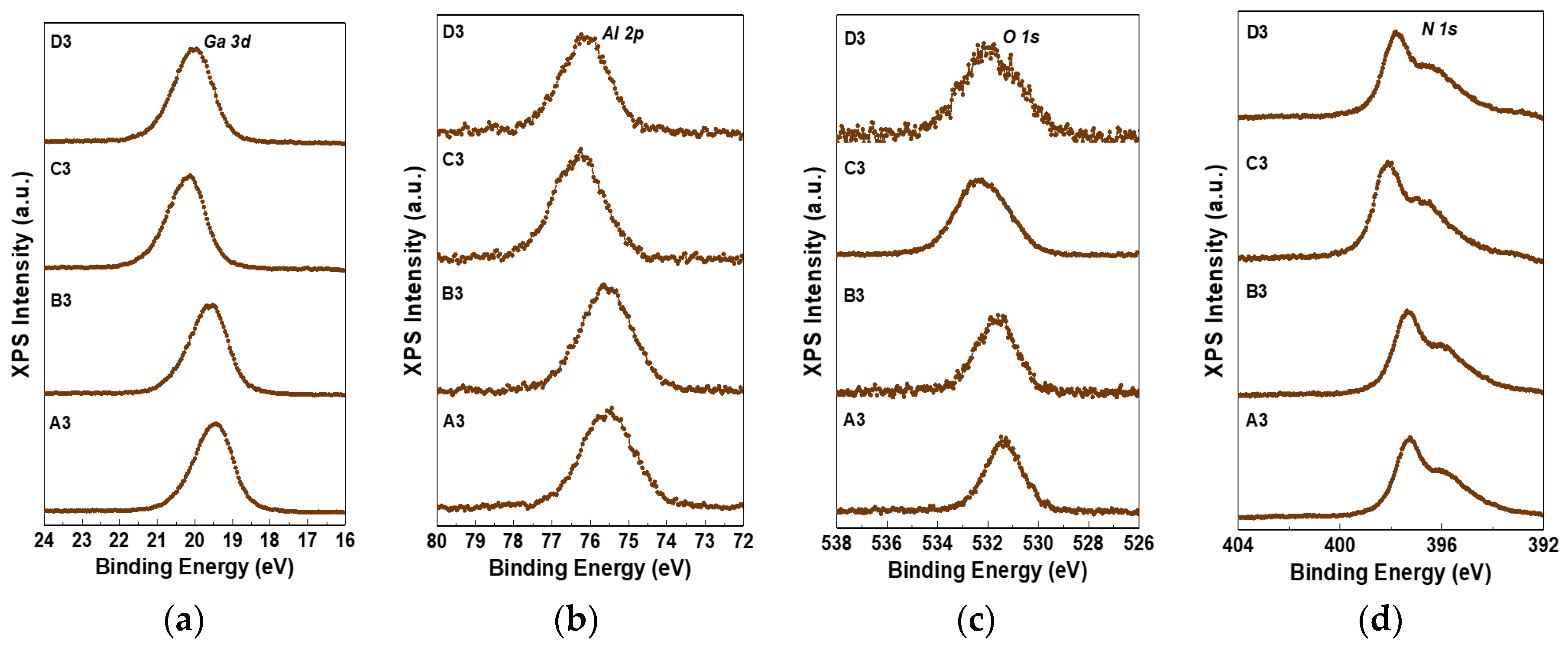
Figure 1. (a) Process steps for GaN Schottky diode (SD): (i) preparation, (ii) atomic-layer deposition (ALD) Al2O3, (iii) post-deposition annealing (PDA), (iv) mesa etching using inductively coupled plasma-reactive ion etching (ICP-RIE), (v) ground metal deposition, (vi) metal area formation through wet etch, (vii) Schottky metal deposition, and (viii) optical image of circular-shaped GaN SD (scale bar = 50 µm). (b) Characterization of surface polarity of GaN using X-ray photoelectron spectroscopy (XPS). (c) XPS spectra of Ga 3d core levels in as-prepared and as-cleaned GaN.
Electronics 09 01068 g001
Figure 2. XPS spectra of (a) Ga 3d, (b) Al 2p, (c) O 1s, and (d) N 1s core levels at 1nm Al2O3/GaN interfaces with post-deposition annealing (PDA) conditions: no anneal (A1), 500 °C for 3 min (B1), 700 °C for 3 min (C1), and 900 °C for 3 min (D1).
Electronics 09 01068 g002
Figure 3. XPS spectra of (a) Ga 3d, (b) Al 2p, (c) O 1s, and (d) N 1s core levels at 3 nm Al2O3/GaN interfaces with PDA conditions: no anneal (A3), 500 °C for 3 min (B3), 700 °C for 3 min (C3), and 900 °C for 3 min (D3).
Electronics 09 01068 g003
Figure 4. Energy band bending at 1 nm Al2O3/GaN interfaces with estimated surface potential (Ψs), valence band offset (VBO), and conduction band offset (CBO) of samples (a) A1, (b) B1, (c) C1, and (d) D1.
Electronics 09 01068 g004
Figure 5. Energy band bending at 3 nm Al2O3/GaN interfaces with Ψs, VBO, and CBO of samples (a) A3, (b) B3, (c) C3, and (d) D3.
Electronics 09 01068 g005
Figure 6. Current density‒voltage (J‒V) characteristics of GaN SDs made from samples as-cleaned (reference), A1, A3, B1, B3, C1, C3, D1, and D3.
Electronics 09 01068 g006
Table 1. Binding energies of core elements at Al2O3/GaN interfaces.
Sample No.Al2O3 (nm)PDA (3 min)Ga 3d (eV)Al 2p (eV)O 1s (eV)N 1s (eV)
A11 nmN. A.19.5575.60531.52397.27
B11 nm500 °C19.7075.74531.65397.41
C11 nm700 °C20.1676.22532.13397.85
D11 nm900 °C20.0176.11532.02397.68
A33 nmN. A.19.5075.56531.48397.23
B33 nm500 °C19.6475.68531.58397.38
C33 nm700 °C20.2276.30532.26397.97
D33 nm900 °C20.0576.16532.14397.81
Table 2. Charge densities at Al2O3/GaN interfaces.
NoSampleAl2O3 Thickness (nm)Anneal Condition (°C, min)GaN Polarity (ND, cm−3)MethodNet Charge Density (cm−2)Interface Charge Density (cm−2)Ref.
1A11-Ga-face (5 × 10¹⁷)XPS−1.19 × 10121.69 × 1013This work
2B11PDA (500, 3)Ga-face (5 × 10¹⁷)XPS−7.79 × 10111.73 × 1013This work
3C11PDA (700, 3)Ga-face (5 × 10¹⁷)XPS2.55 × 10142.73 × 1014This work
4D11PDA (900, 3)Ga-face (5 × 10¹⁷)XPS1.38 × 10133.19 × 1013This work
5A33-Ga-face (5 × 10¹⁷)XPS−1.28 × 10121.68 × 1013This work
6B33PDA (500, 3)Ga-face (5 × 10¹⁷)XPS−9.98 × 10111.71 × 1013This work
7C33PDA (700, 3)Ga-face (5 × 10¹⁷)XPS8.20 × 10148.38 × 1014This work
8D33PDA (900, 3)Ga-face (5 × 10¹⁷)XPS3.00 × 10134.81 × 1013This work
9S1--Ga-face (4 × 10¹⁷)XPS2.09 × 10122.01 × 1013Ref. [8]
10S2--Ga-face (4 × 10¹⁷)XPS−1.0 × 10121.7 × 1013Ref. [8]
11-6, 12, 18PDA (600, 3),
PMA (400, 5)
Ga-face (1 × 10¹⁸)C-V4.60 × 10122.27 × 1013Ref. [26]
12-6, 12, 18PDA (700, 1)Ga-face (1 × 10¹⁸)C-V9.5 × 10122.7 × 1013Ref. [27]
13-6, 12, 18PDA (700, 1),
PMA (400, 5)
Ga-face (1 × 10¹⁸)C-V4.1 × 10122.2 × 1013 (estimated)Ref. [27]
14-6, 12, 18PDA (700, 1),
PMA (450, 5)
Ga-face (1 × 10¹⁸)C-V2.2 × 10122.0 × 1013 (estimated)Ref. [27]
15-6, 12, 18PDA (700, 1),
PMA (500, 5)
Ga-face (1 × 10¹⁸)C-V1.1 × 10121.9 × 1013Ref. [27]
16-6, 12, 18PDA (700, 1),
PMA (400, 5)
N-face (1 × 10¹⁸)C-V9.2 × 10122.7 × 1013 (estimated)Ref. [27]
17-6, 12, 18PDA (700, 1),
PMA (450, 5)
N-face (1 × 10¹⁸)C-V5.9 × 10122.4 × 1013 (estimated)Ref. [27]
18-6, 12, 18PDA (700, 1),
PMA (500, 5)
N-face (1 × 10¹⁸)C-V2.8 × 10122.0 × 1013 (estimated)Ref. [27]
19-6, 12, 18PDA (700, 1),
PMA (550, 5)
N-face (1 × 10¹⁸)C-V9.0 × 10111.9 × 1013 (estimated)Ref. [27]
20-6, 12, 18PDA (700, 1)m-plane (6 × 10¹⁶)C-V7.8 × 10122.5 × 1013 (estimated)Ref. [27]
21-6, 12, 18PDA (700, 1),
PMA (400, 5)
m-plane (6 × 10¹⁶)C-V2.5 × 10122.0 × 1013 (estimated)Ref. [27]

