Article

Polarization-Charge Inversion at Al2O3/GaN Interfaces through Post-Deposition Annealing


1
Department of Electronic and Electrical Convergence Engineering, Hongik University, Sejong 30016, Korea
2
School of Electronics Engineering, Kyungpook National University, Daegu 41566, Korea
*
Authors to whom correspondence should be addressed.
Electronics 2020, 9(7), 1068; https://doi.org/10.3390/electronics9071068

Submission received: 2 June 2020 / Revised: 20 June 2020 / Accepted: 29 June 2020 / Published: 30 June 2020
(This article belongs to the Special Issue Applications of Thin Films in Microelectronics)

Abstract

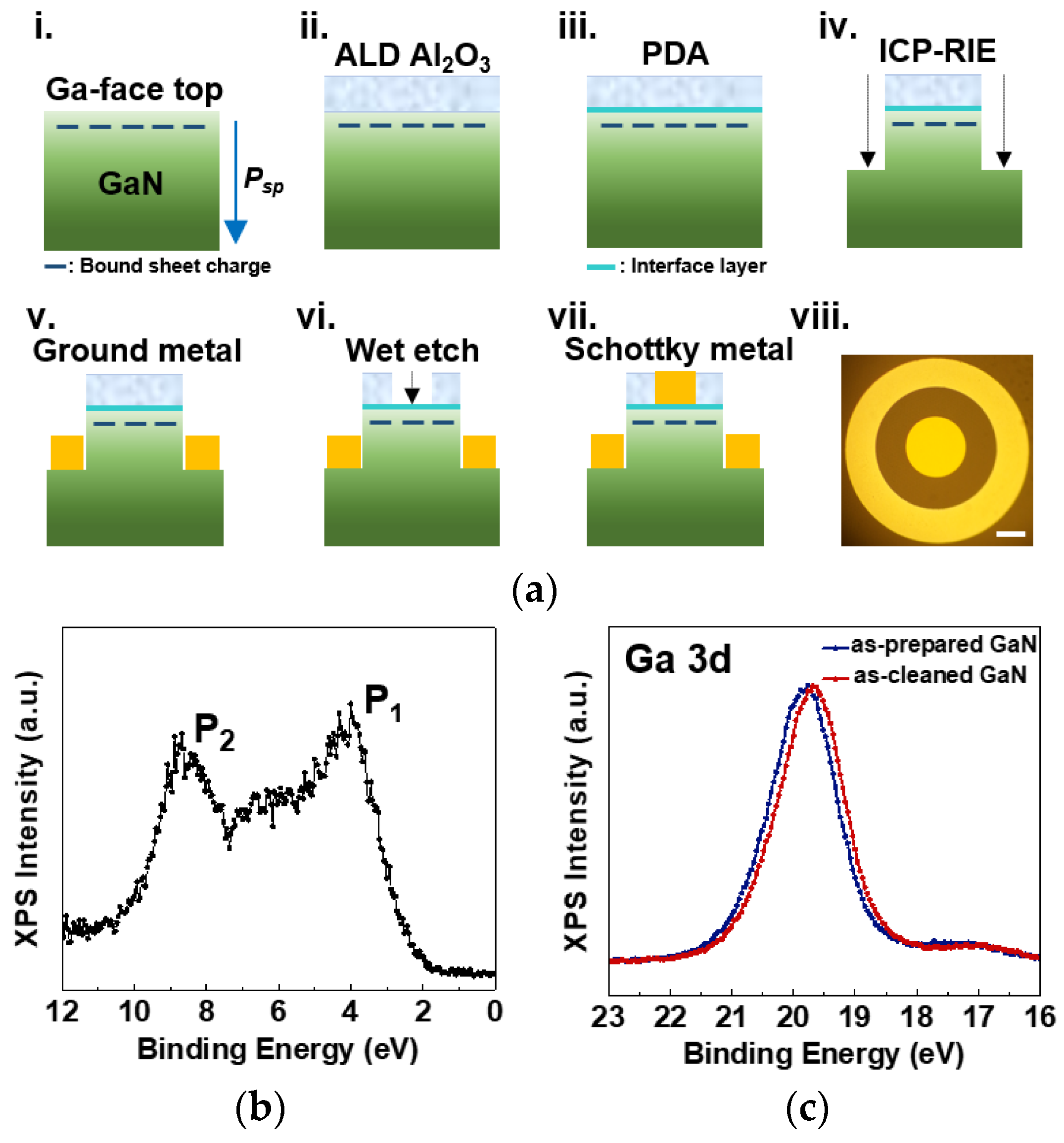
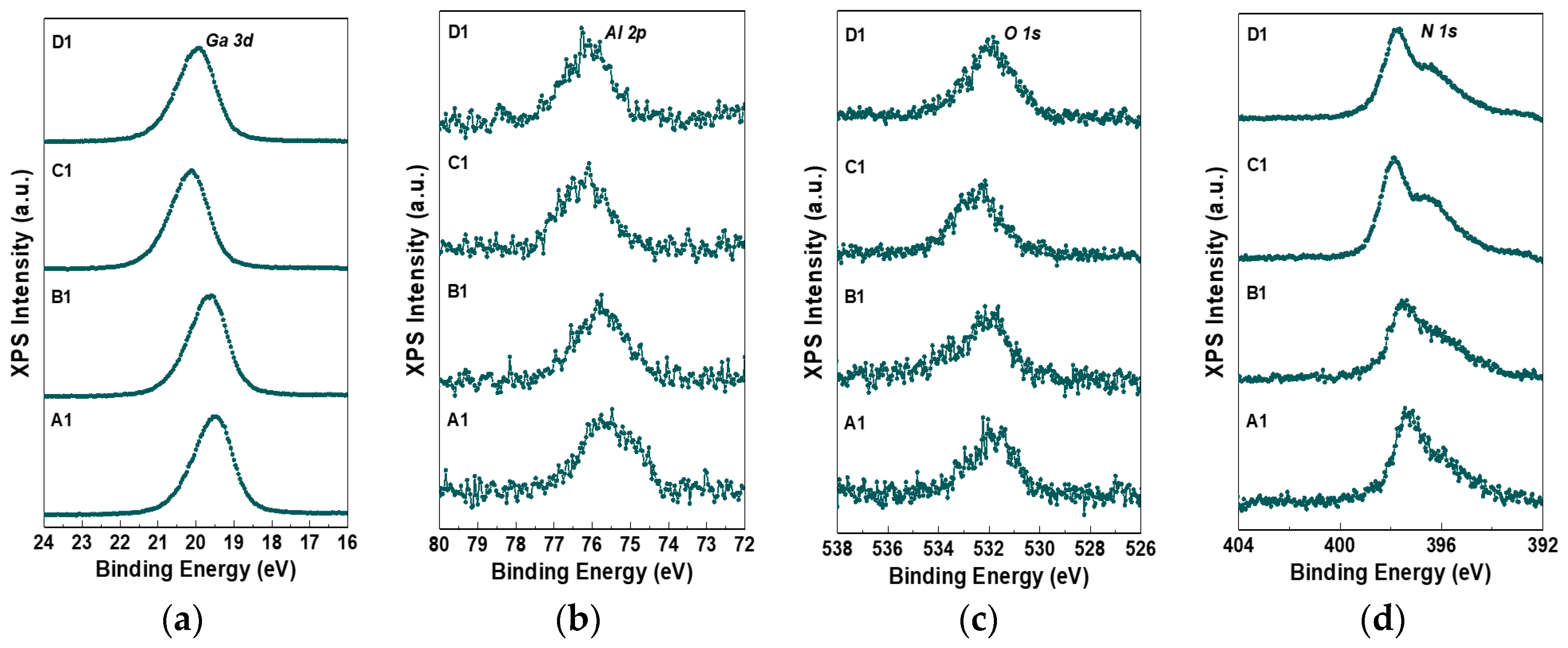
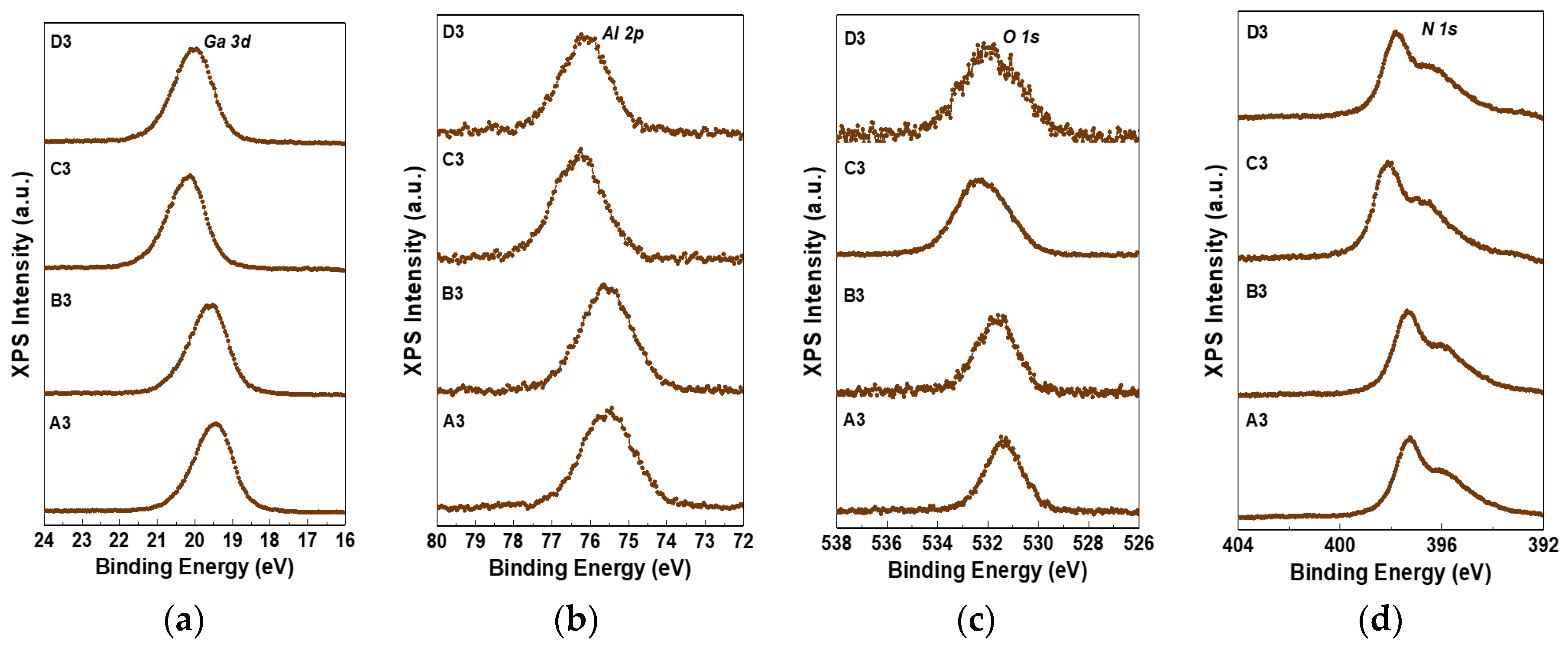
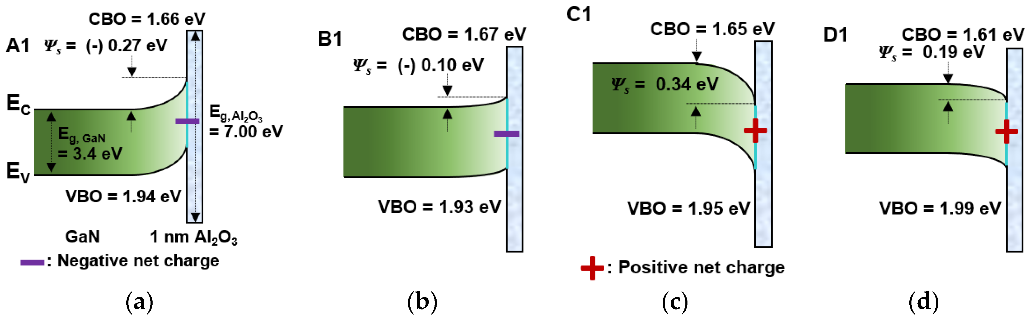
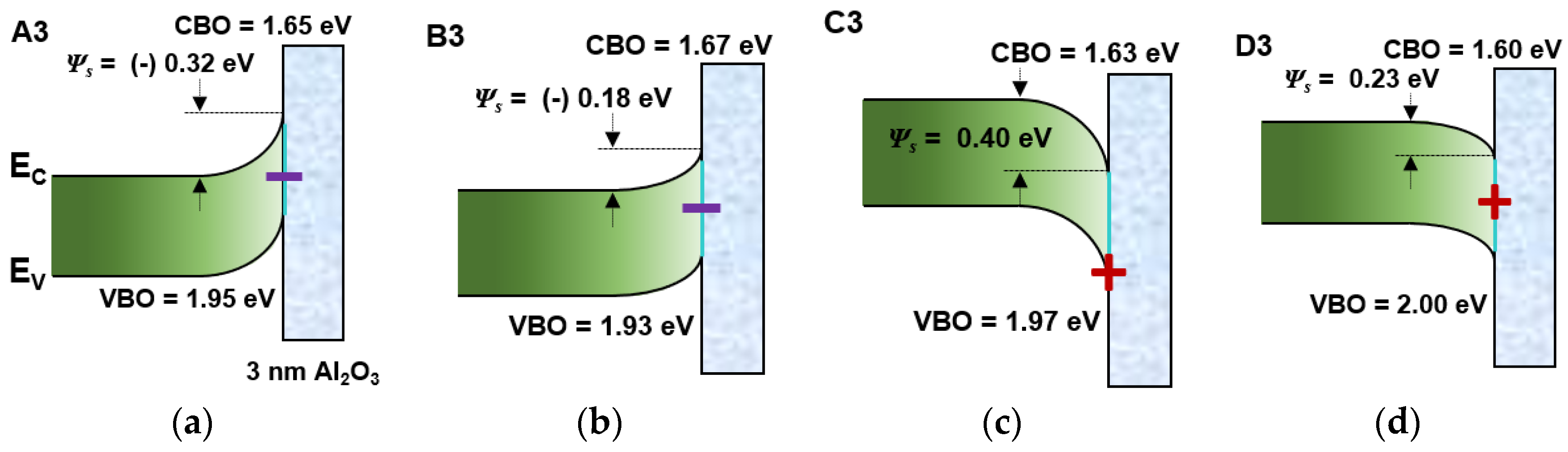
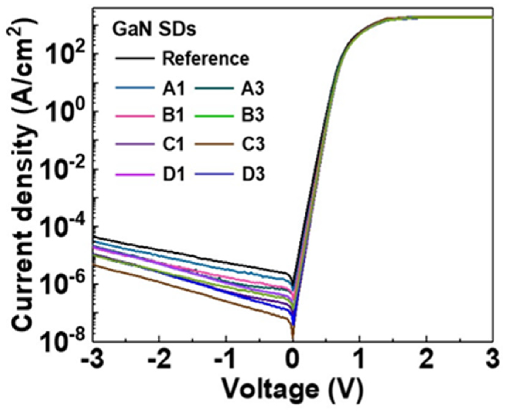
The effects of post-deposition annealing (PDA) on the formation of polarization-charge inversion at ultrathin Al2O3/Ga-polar GaN interfaces are assessed by the analysis of energy band bending and measurement of electrical conduction. The PDA-induced positive interface charges form downward energy band bending at the Al2O3/GaN interfaces with polarization-charge inversion, which is analyzed using X-ray photoelectron spectroscopy. Net charge and interface charge densities at the Al2O3/GaN interfaces are estimated after PDA at 500 °C, 700 °C, and 900 °C. The PDA temperatures affect the formation of charge densities. That is, the charge density increases up to 700 °C and then decreases at 900 °C. Electrical characteristics of GaN Schottky diodes with ultrathin Al2O3 layers exhibit the passivation ability of the Al2O3 surface layer and the effects of polarization-charge inversion through PDA. This result can be applied to improvement in GaN-based electronic devices where surface states and process temperature work important role in device performance.
Keywords: post-deposition annealing; Al2O3/GaN; interface charge density; polarization-charge inversion post-deposition annealing; Al2O3/GaN; interface charge density; polarization-charge inversion