Article

Effect of Mg Doping on the Electrical Performance of a Sol-Gel-Processed SnO2 Thin-Film Transistor

1
School of Electronics Engineering, Kyungpook National University, Daegu 41566, Korea
2
Department of Electronic and Electrical Convergence Engineering, Hongik University, Sejong 30016, Korea
*
Author to whom correspondence should be addressed.
Electronics 2020, 9(3), 523; https://doi.org/10.3390/electronics9030523
Submission received: 7 March 2020 / Revised: 20 March 2020 / Accepted: 20 March 2020 / Published: 22 March 2020
(This article belongs to the Special Issue Applications of Thin Films in Microelectronics)

Abstract

:
Sol-gel-processed Mg-doped SnO2 thin-film transistors (TFTs) were successfully fabricated. The effect of Mg concentration on the structural, chemical, and optical properties of thin films and the corresponding TFT devices was investigated. The results indicated that an optimal Mg concentration yielded an improved negative bias stability and increased optical band gap, resulting in transparent devices. Furthermore, the optimal device performance was obtained with 0.5 wt% Mg. The fabricated 0.5 wt% Mg-doped SnO2 TFT was characterized by a field effect mobility, a subthreshold swing, and Ion/Ioff ratio of 4.23 cm2/Vs, 1.37 V/decade, and ~1 × 10⁷, respectively. The added Mg suppressed oxygen-vacancy formation, thereby improving the bias stability. This work may pave the way for the development of alkaline-earth-metal-doped SnO2-based thin-film devices.

1. Introduction

Oxide semiconductor-based thin-film transistors (TFTs) have attracted considerable attention due to their potential application in next-generation displays, including transparent displays, transparent sensors, and electrochromic windows [1,2,3,4]. To date, indium-based metal-oxide systems, such as InGaZnO, ZrInZnO, InGaO, and InZnO, have been used for these transistors, which exhibit high mobility. Indium-based metal-oxide TFTs can be fabricated through a low-temperature process, unlike conventional polysilicon or amorphous silicon-based thin-film transistors [5,6,7,8]. Unfortunately, In is a costly rare metal found in only a few mining sites worldwide [9]. Thus, finding a new metal oxide system consisting of non-rare metals is critical for high-performance transparent novel devices. Tin dioxide (SnO2) is easily crystallized due to its low melting temperatures and has a high intrinsic mobility, and large band gap (3.6 eV), and is therefore considered a promising candidate for replacing indium-based oxide semiconductors. In addition, the electronic configuration of Sn (1s22s2p63s2p6d105s2p2) is similar to that of In (1s22s2p63s2p6d104s2p6d105s2p1) [10]. Owing to these attributes, TFTs fabricated with SnO2 are characterized by excellent electrical properties [11,12,13]. Unfortunately, metal-oxide-based TFTs are prone to electrical instability due to various factors, such as ambient light, external bias voltage, and environmental gases. The instability originates from charge trap sites with oxygen vacancies or other defect sites [14,15,16]. To overcome this drawback, an oxygen vacancy suppressor can be added to the material. Oxygen vacancies can act as carriers as well as defects, thereby causing instability.
Metal-oxide-based devices are usually fabricated with vacuum-based equipment, which hinders the low-cost fabrication of large area devices [17,18,19]. As a result, simple techniques that can be performed without complex and expensive vacuum systems have been introduced. The sol-gel process is relatively simple and is therefore considered a promising deposition process. The composition ratio of each component comprising the solution can be easily controlled. In addition, the liquid phase precursors can be applied as inks for spin coating, inkjet printing, and gravure printing, without the use of expensive vacuum and pumping systems [12,13,20]. In the work reported here, we describe the first-ever Mg-doped SnO2 TFTs fabricated by means of a sol-gel method. Added Mg was used as a carrier suppressor for reducing the density of oxygen defects. The electrical and optical properties of Mg-doped SnO2 thin films were investigated. The 0.5 wt% Mg-doped SnO2 TFTs exhibited satisfactory stability and a field effect mobility of 4.5 cm2/Vs with good negative bias stress (NBS) properties. Although alkaline earth-metal-doped SnO2 thin films have been previously studied, published reports on the electrical characteristics of Mg-doped SnO2 TFTs are rare. This work may pave the way for the development of alkaline earth-metal-doped SnO2-based thin-film devices.

2. Materials and Methods
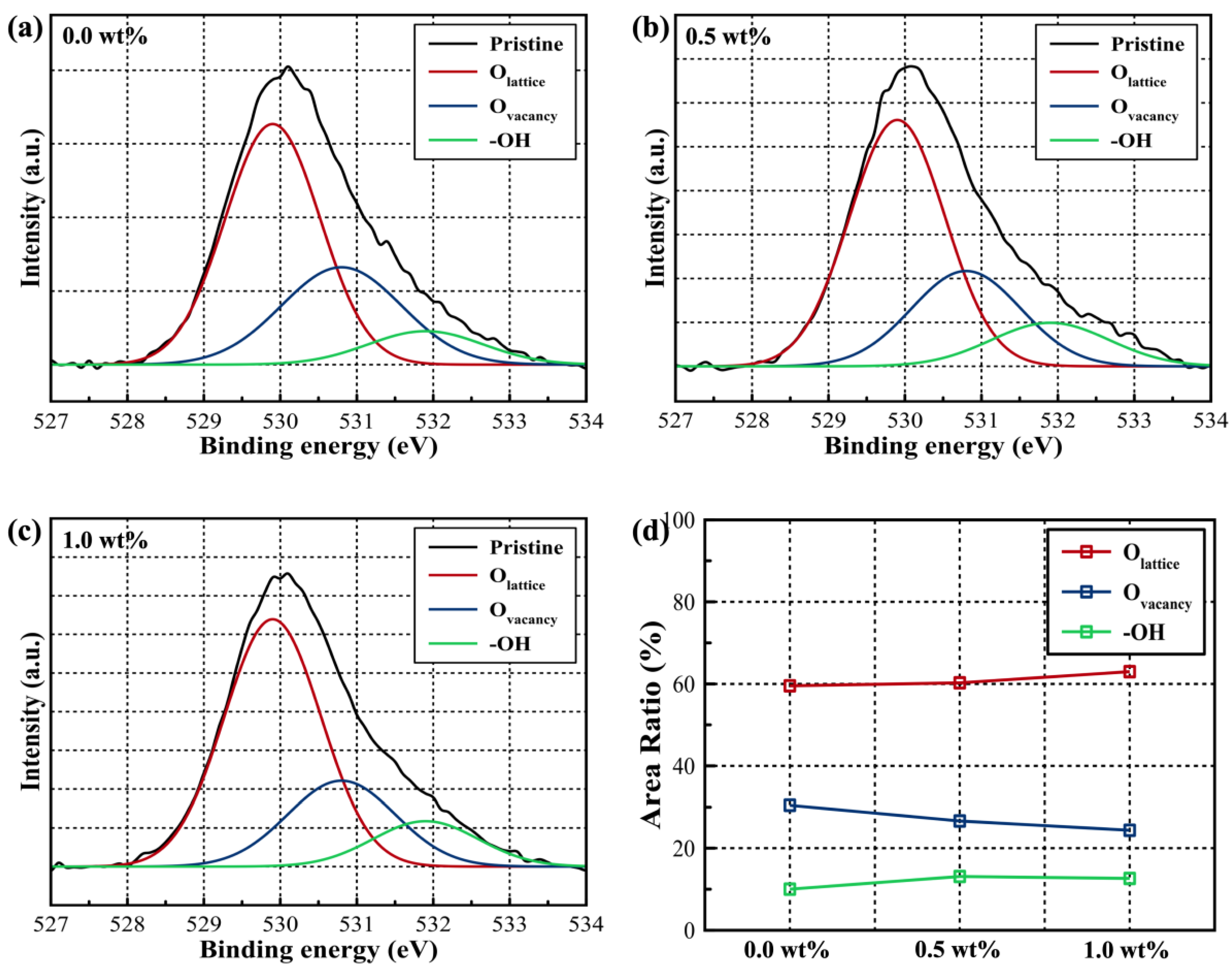
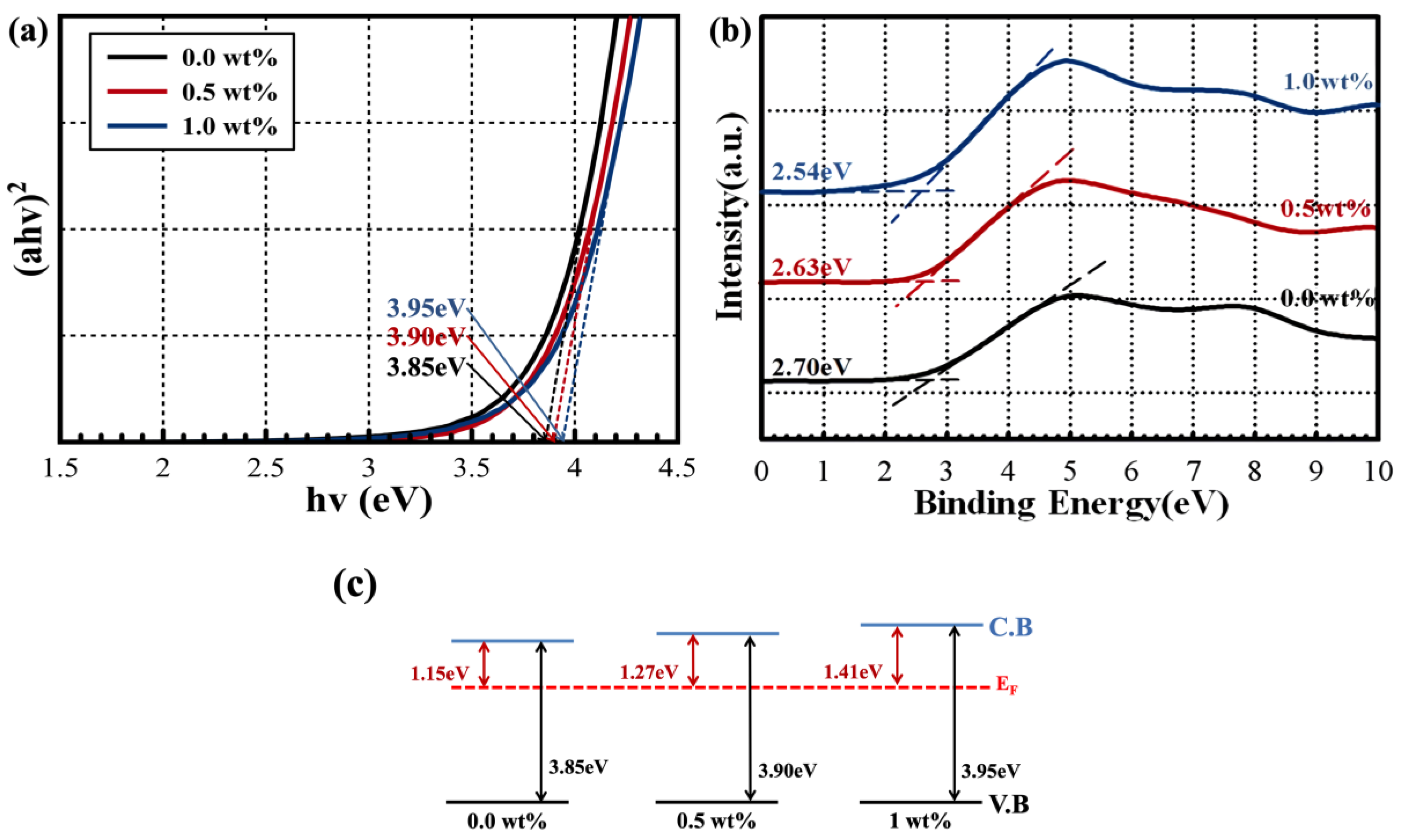
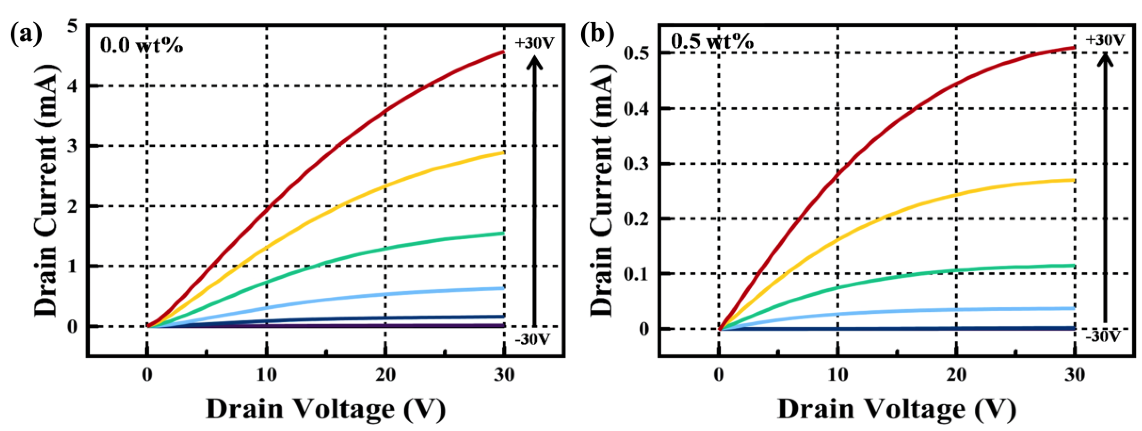
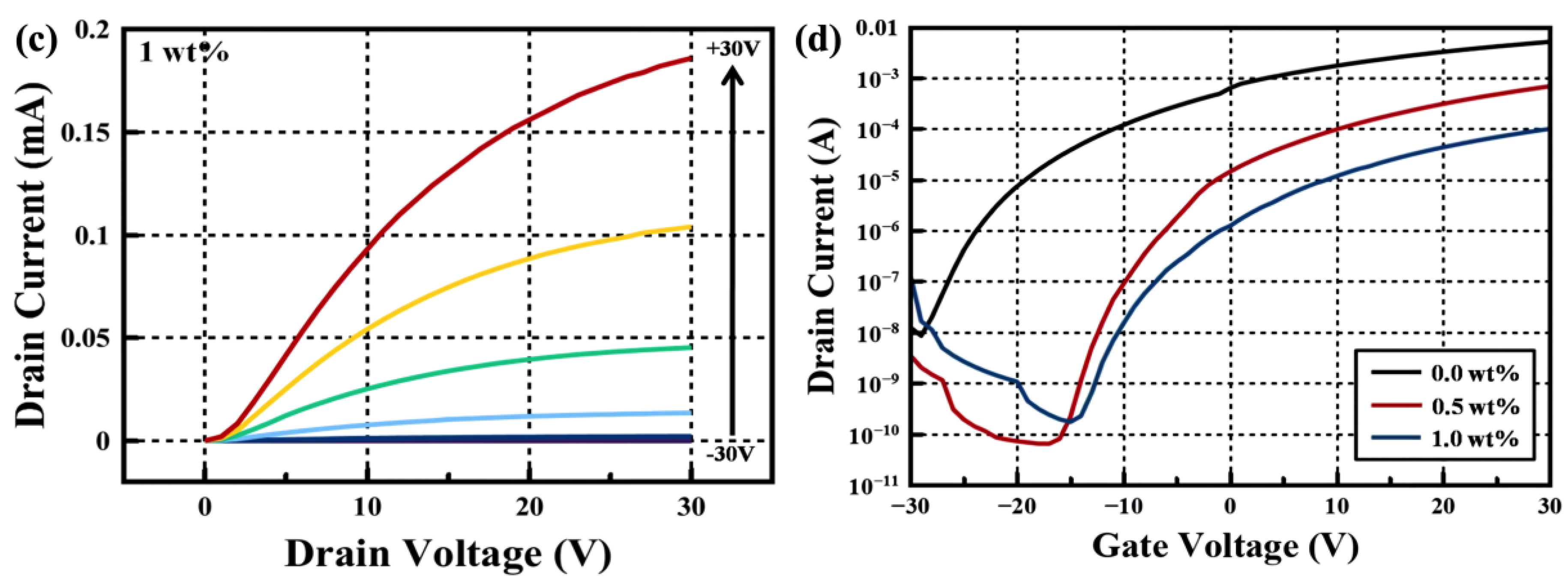
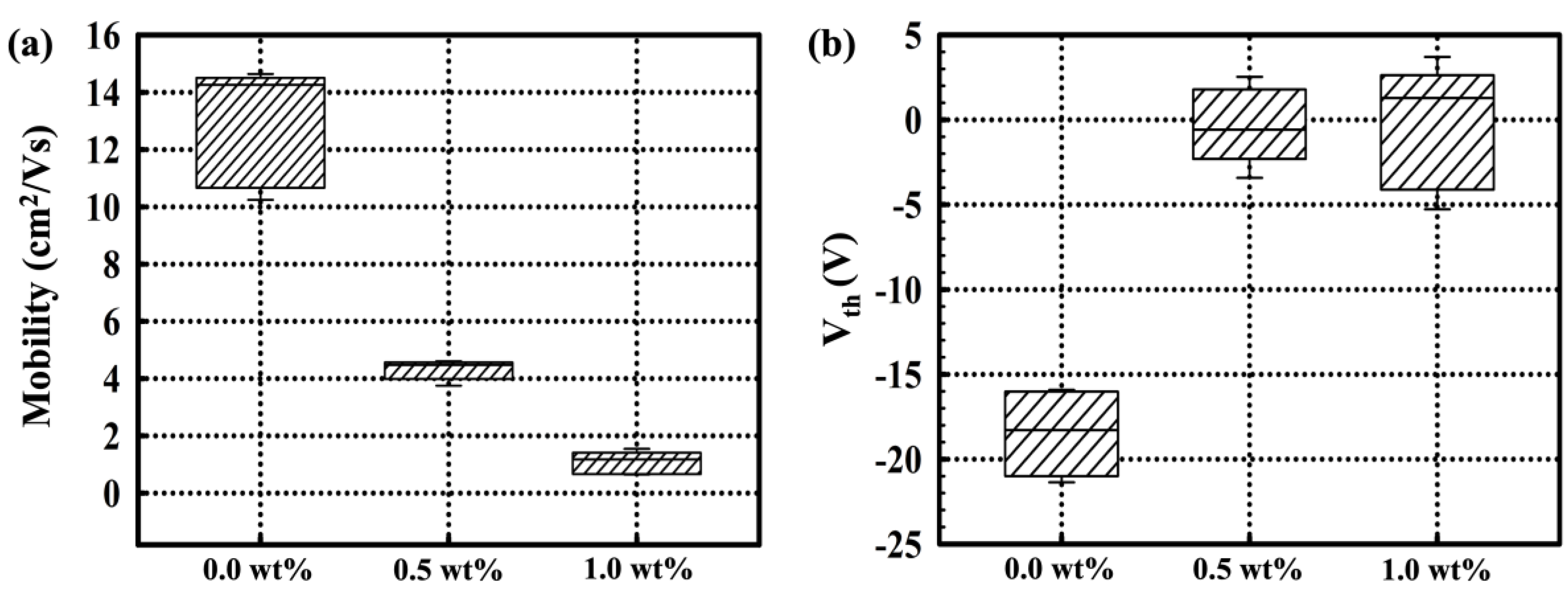
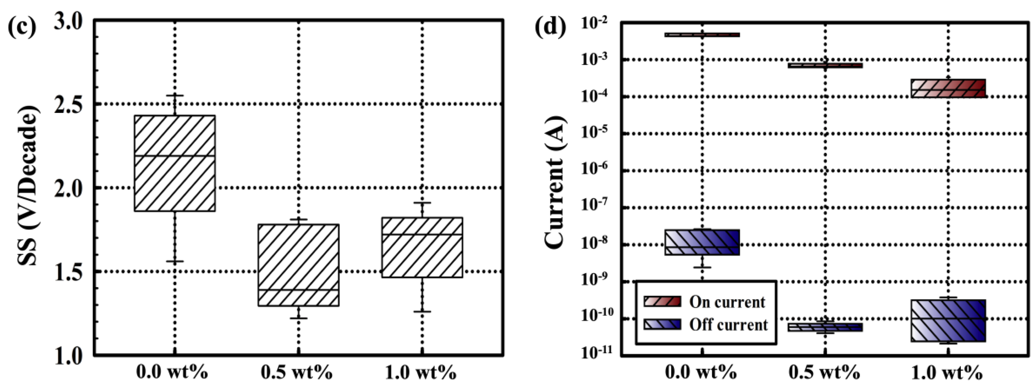
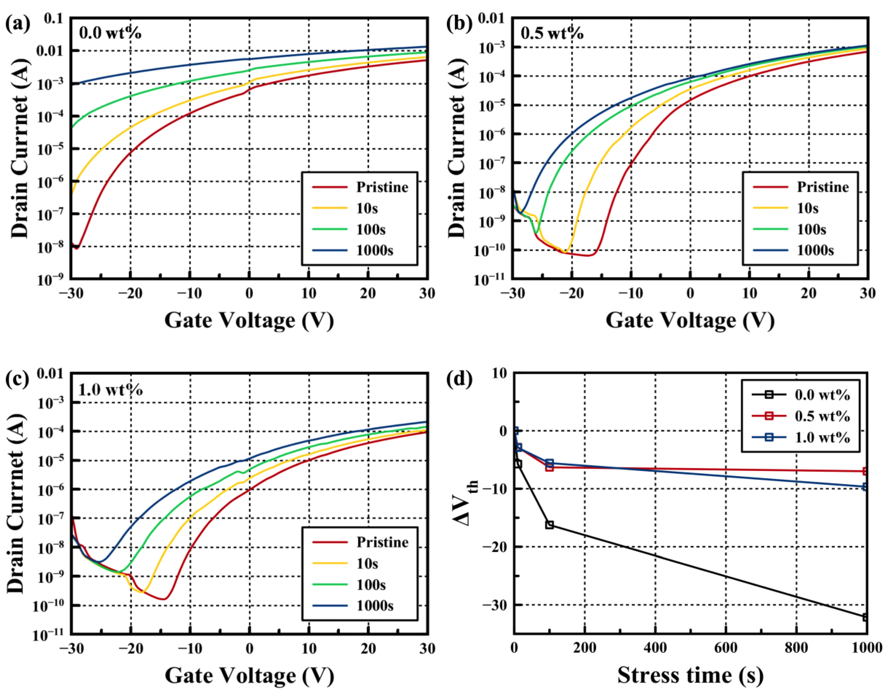
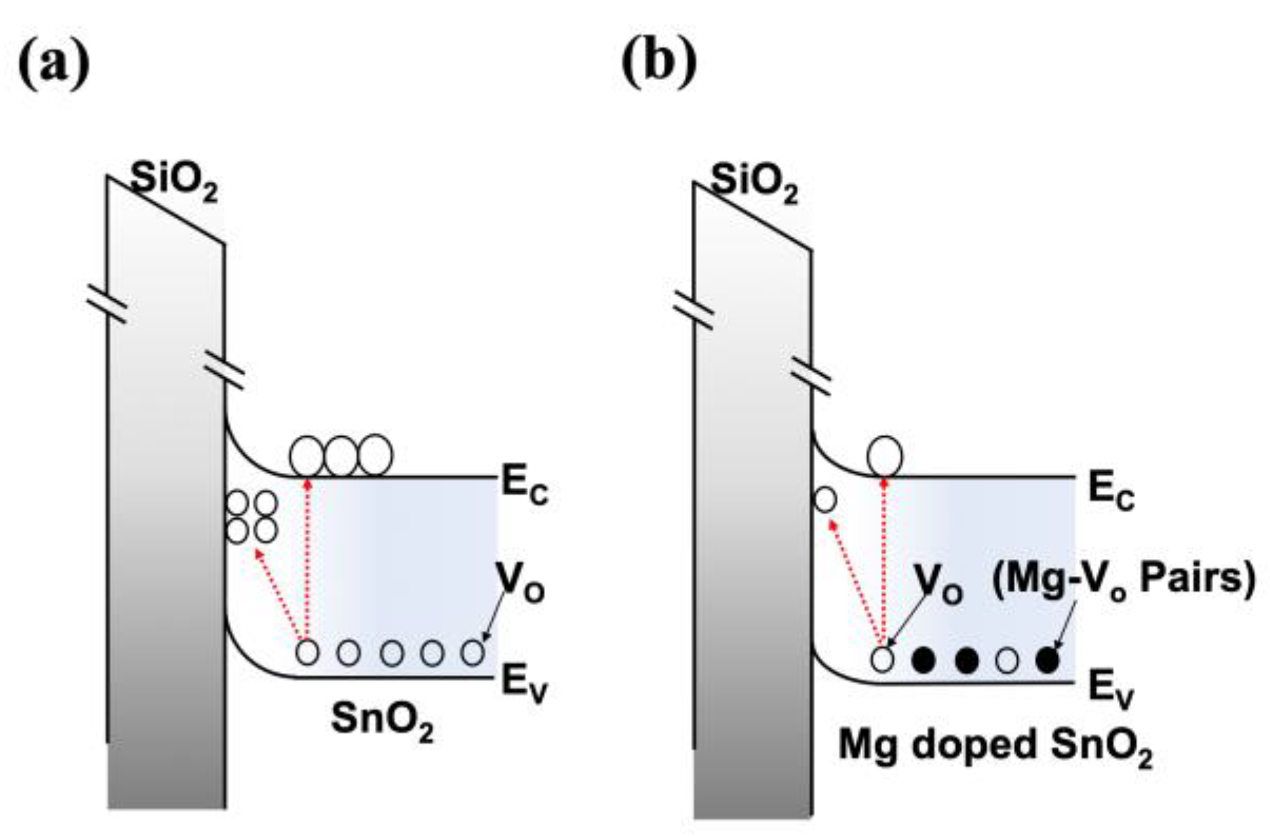
All reagents in this study including the tin (II) chloride dehydrate (SnCl2∙2H2O) and the magnesium nitrate hexahydrate (Mg(NO3)2∙6H2O) were purchased from Sigma Aldrich. The SnCl2∙2H2O and Mg(NO3)2∙6H2O were dissolved in ethanol to a concentration of 0.03 M. Two different concentrations (0.5 and 1 wt%) of Mg(NO3)2∙6H2O solutions were dissolved in a prepared SnO2 precursor. We fabricated the TFTs with an inverted coplanar structure. A heavily doped p-type silicon was used as the substrate and a gate electrode with a thermally grown 100-nm-thick silicon dioxide layer was used as the gate dielectric. The substrates were cleaned using a UV/O3 cleaner for 10 min. The 50-nm-thick Au source/drain electrodes were deposited by an e-beam evaporator and patterned via the lift-off method. SnO2 with/without Mg semiconductor layers was deposited by means of a spin-coating process performed at 3000 rpm for 50 s. The spin-coated films were pre-annealed at 150 °C for 10 m and post-annealed for 1 h at 500 °C using a hot plate. The coated films were patterned using mechanical elimination for full isolation that prevents fringing effects and a gate leakage current. The phase and structural properties of the films were investigated by means of X-ray reflectivity (XRR; PANalytical Empyrean) and grazing incidence X-ray diffraction (GIXRD; Philips X’pert Pro) measurements. A small incident angle (0.3°) and fixed CuKα radiation (λ = 154.06 pm) were employed. Furthermore, X-ray photoelectron spectroscopy (XPS; ULVAC-PHI) was used to evaluate changes in the chemical composition of the films. A monochromatic AlKα (1488 eV) source was used as the X-ray source. The base pressure of the chamber was maintained at 4 × 10⁻⁷ Pa, and the pass energy was 40 eV. The optical properties needed for calculation of the optical band gap were obtained through ultraviolet-visible spectroscopy (UV-Vis; LAMBDA 265) measurements. The electrical characteristics of the fabricated TFTs at room temperature in air were obtained using an Agilent 4155 semiconductor parameter analyzer and a probe station.

3. Results

Figure 1a shows the GIXRD spectra of solution-processed SnO2 films associated with different Mg doping concentrations (0–1 wt%). All films are polycrystalline phase SnO2 with a tetragonal structure, consistent with pure SnO2 thin films (JCPDS card number: 41-1445). The peaks of other phases, such as MgO and SnxMgyO, are absent from the patterns. The diffraction peaks at 26.61°, 33.89°, 37.95°, and 51.78° correspond to the (110), (101), (200), and (211) crystal planes, respectively, of the SnO2 tetragonal structure. The full width at half-maximum (FWHM) of a GIXRD peak is closely correlated with the crystallite size of a specific crystal orientation. The GIXRD results indicate that the FWHM of the SnO2 (110) plane is smaller than the FWHM of the other planes and, hence, SnO2 crystallites grow mainly in the (110) plane. Figure 1a confirms that the intensity of each peak increases with increasing Mg doping concentration.
The ionic radii of Sn4+ (0.69 Å) and Mg2+ (0.72 Å) are almost identical and, hence, the lattice parameters are unaffected by the Mg doping concentration. The crystallite sizes of the SnO2 films are estimated from Scherrer’s formula, D = 0.9λ/(βcos θ), where D is the crystallite size, λ is the Cu Κα wavelength (1.54 Å), β is the FWHM of the peak, and θ is the peak position. The SnO2 crystallite size slightly increases after Mg doping [21]. Crystallite sizes of 7.68, 7.83, and 8.36 nm for 0.0, 0.5, and 1 wt% doping, respectively, are calculated at the (110) plane. The density of SnO2 films doped at concentrations ranging from 0 to 1 wt% was determined by means of XRR analysis (see Figure 1b). The film density for total external reflection is determined by the critical angle, i.e., the density increases with increasing values of this angle. Critical angles of 0.261°, 0.286°, and 0.278° as well as film densities (determined via Buyden’s method) of 3.70, 4.43, and 4.18 g/cm3 are obtained for doping concentrations of 0.0, 0.5, and 1 wt%, respectively. That is, the largest density is obtained for the 0.5 wt% Mg-doped SnO2 film (see Table 1 for the measured structural properties of the SnO2 thin films).
Figure 2 shows the O 1s peak of XPS spectra corresponding to 0–1 wt% Mg doping concentrations. The binding energy (BE) of each element was calibrated based on the C 1s peak at 284.6 eV. We analyzed the O 1s peaks, which consisted of three sub-peaks associated with lattice oxygen (OL: Olattice), oxygen vacancies (OV: Ovacancy), and hydroxide impurities (-OH). The OV and OL peaks vary with increasing Mg doping concentration, with the corresponding intensities decreasing slightly from 30.45% to 24.38% and increasing from 59.53% to 62.98%, respectively. The -OH peak changes, but these changes appear to be somewhat random. Dopants acting as carrier suppressors are characterized by several properties. For example, the electronegativity of the dopants should differ significantly from the electronegativity of oxygen (3.44). A relatively low standard electrode potential (SEP) results in increasing the bond strength of dopant-oxygen bonds. The bond strength of metal-oxygen is also crucial for enhancing the stability of TFTs by controlling oxygen vacancies [22]. Other important properties of the dopant include the ionic radius, effective nuclear charge, and Lewis acid strength (L) [23]. Mg dopants have lower electronegativity and SEP (1.31, −2.37 V) than their Sn hosts (1.96, −0.14 V). Thus, the addition of Mg dopants as oxygen binders leads to the suppression of oxygen vacancies to secure good bias properties because they are more strongly combined with oxygen.
Figure 3 shows the optical band gap measured via UV-VIS. In addition, Figure 3b,c show the XPS-measured valence band (VB) spectra and the schematic energy band diagram of Mg-doped SnO2 with 0–1 wt% Mg doping concentrations. The optical band gap is widened from 3.85 eV to 3.95 eV with increasing Mg doping concentration, as shown in Figure 3a. As the concentration increases, the optical band gap increases, consistent with the results of a previous study. Figure 3b shows that the VB offset between the VB maximum value and the Fermi level decreases from 2.70 eV to 2.54 eV with increasing Mg doping concentration. Based on these results, we confirmed that the conduction band (CB) offset between the CM minimum value and the Fermi level increases from 1.15 eV to 1.41 eV and the carrier concentration decreases depending on the doping concentration [24]. The band gap of defect-containing SnO2 is smaller than that of defect-free SnO2 due to the increase in VB and narrowing of the band gap induced by the homogeneous oxygen vacancies. As the Mg doping concentration increases, the density of oxygen vacancies can be reduced, leading to VB reduction and band gap widening [25].
Figure 4 shows the output curves measured in air after fabrication of the SnO2 TFTs at different Mg doping concentrations. The drain current versus drain voltage (ID-VD) curves of the TFTs were measured at different gate voltages (VG) ranging from –30 V to +30 V with an increment of 10 V. The curves shown in Figure 4a–c correspond to typical n-type semiconductors with normally on state electrical properties. The on-current is reduced by the changing carrier concentration at increasing Mg doping concentrations. At a low VD, the ID-VD plots are non-linear, owing to Schottky barrier formation induced by the large work function difference between the n-type SnO2 and the Au source/drain electrodes [26].
Figure 4d shows the corresponding transfer characteristics of the SnO2 TFTs with respect to Mg doping concentration. The drain current at a drain voltage of +30 V is measured as a function of the gate voltage, ranging from −30 V to +30 V. The saturation mobility (μ) and the subthreshold swing (SS) are calculated from the following equations for a typical transistor:
I D = μ C i W 2 L ( V g V t h ) 2
S S = ( δ l o g I D δ V G ) 1
where, Ci is the capacitance per unit area of the oxide gate insulator, W and L are the channel width and length, respectively, Vth is the threshold voltage, VG is the gate voltage, and ID is the drain current. The Vth was obtained from the intercept of the fitting line used, when we extract the mobility in the saturation regime from Equation (1). The extracted parameters for the SnO2 TFTs with different Mg concentrations are plotted in Figure 5.
The extracted saturation mobilities of the 0, 0.5, and 1 wt% Mg-doped transistors were 13.84, 4.23, and 0.67 cm2/Vs, respectively. Degradation of the saturation mobility is revealed by the O 1s peak of the XPS spectra and energy band diagrams of the extracted UV-vis and XPS spectra, as shown in Figure 2 and Figure 3. The density of oxygen vacancies decreases with Mg dopants combined with oxygen. The suppression of oxygen vacancies leads to a decline in the carrier concentration. Moreover, we verified that the CB offset of the energy band diagram broadens from 1.15 eV to 1.41 eV with increasing Mg-doping concentration. Consequently, the carrier concentration decreases considerably. The decrease in the saturation mobility is also correlated with the crystalline size of each SnO2 TFT. Generally, the number of grain boundary increases with decreasing crystalline size. Many grain boundaries play a role in surface scattering, thereby resulting in the deterioration of saturation mobility [27]. However, a different trend is observed in this study. The main carrier transport mechanism operating inside metal-oxide semiconductors is the percolation conduction mechanism that can be improved by filling the trap state at high carrier concentrations [28]. The field effect mobility and on-current are proportional to the carrier concentration. The assumption is that the effect of saturation mobility reduction induced by carrier-concentration reduction is greater than the effect of the reduction induced by surface scattering. The on/off current ratios are all >105 and the extracted SSs for 0, 0.5, and 1 wt% doping are 2.16, 1.37, and 1.92 V/decade, respectively. The difference in SS is dominant, owing to the influence of the trap density in each film. Figure 6 shows the transfer curves of the respective TFTs under a negative bias stress (NBS). The NBS measurement of the non-passivated SnO2 TFTs in the air is evaluated for 1000 s at a gate voltage of −30 V and a drain voltage of +5 V. In the NBS condition, the Vth of the TFTs for Mg doping concentrations of 0, 0.5, and 1 wt% shifts −32.13 V, −6.99 V, and −9.85 V, respectively, in the negative direction The Vth shift is lowest for the 0.5 wt% Mg-doped SnO2 TFTs. According to the above-mentioned XPS results, the Mg dopants have lower electronegativity and SEP than their Sn hosts. Therefore, the defect-related oxygen vacancies in the SnO2 thin-film are reduced and the lattice bonding of metals is increased, resulting in decreased field effect mobility and improved bias stability.
Figure 7 shows a schematic of the degradation mechanism for TFTs under NBS. The negatively shifted Vth originates from the trapping of positive charges at dielectric/semiconductor interfaces. Furthermore, trapping of the positive charges results from the ionization of the oxygen vacancies (VO→ VO2++2e-) inside semiconductor layers and VO2+ immigration to the interface after NBS. The introduction of Mg leads to a decrease in the density of oxygen vacancies in the semiconductor through the formation of Mg-VO pairs. Negative shifts of Vth and degraded SS imply defect-state generation or redistribution. These defect states may exist in the deep levels.
In addition, the negative shift of Vth in a non-passivated SnO2 TFT is strongly influenced by the moisture absorption mechanism. The film qualities, such as the density and porosity, can determine the sensitivity to absorption molecules. In the above results, the decrease in the Vth shift is attributed to multiple effects resulting from the decrease in oxygen vacancies. This decrease results from changes in the density of the SnO2 thin-film due to the added Mg dopants. The 0.5 wt% Mg-doped SnO2 thin-film, with its high density and densely packed structures with relatively small contact areas, prevented the adsorption of water molecules and yielded improvement in the NBS.

4. Conclusions

In the present work, Mg-doped SnO2 TFTs are successfully fabricated by means of a sol-gel process. The effect of Mg concentration on the structural, chemical, and optical properties of thin films and the corresponding TFT devices is investigated. Controlling the oxygen vacancies and density of the films with added Mg, yields the optimal device performance at 0.5 wt% Mg. The fabricated 0.5 wt% Mg-doped SnO2 TFT is characterized by a field effect mobility, SS, and Ion/Ioff ratio of 4.23 cm2/Vs, 1.37 V/decade, and ~1 × 10⁷, respectively. The added Mg suppresses oxygen-vacancy formation and improves bias stability. This work may pave the way for the development of alkaline-earth-metal-doped SnO2-based thin-film devices.

Author Contributions

Conceptualization, W.-Y.L. and J.J.; experiments and data analysis, W.-Y.L., H.L., S.H., C.L.; investigation, W.-Y.L., H.L., S.H.; writing—original draft preparation, W.-Y.L. and J.J.; writing—review and editing, J.-H.B., I.-M.K., K.K. and J.J. All authors have read and agreed to the published version of the manuscript.

Funding

This research was supported by the Basic Science Research Program through the National Research Foundation of Korea (NRF) grant funded by the Korea government (MSIT) (2019R1F1A1059788).

Conflicts of Interest

The authors declare no conflicts of interest.

References

  1. Nomura, K.; Ohta, H.; Takagi, A.; Kamiya, T.; Hirano, M.; Hosono, H. Room-temperature fabrication of transparent flexible thin-film transistors using amorphous oxide semiconductors. Nature 2004, 432, 488–492. [Google Scholar] [CrossRef] [PubMed]
  2. Yabuta, H.; Sano, M.; Abe, K.; Aiba, T.; Den, T.; Kumomi, H.; Nomura, K.; Kamiya, T.; Hosono, H. High-mobility thin-film transistor with amorphous InGaZnO4 channel fabricated by room temperature rf-magnetron sputtering. Appl. Phys. Lett. 2006, 89, 112123. [Google Scholar] [CrossRef]
  3. Tomai, S.; Nishimura, M.; Itose, M.; Matuura, M.; Kasami, M.; Matsuzaki, S.; Kawashima, H.; Utsuno, F.; Yano, K. Highperformance thin-film transistor with amorphous In2O3–SnO2–ZnO channel layer. Jpn. J. Appl. Phys. 2012, 51, 03CB01. [Google Scholar] [CrossRef]
  4. Ebata, K.; Tomai, S.; Tsuruma, Y.; Iitsuka, T.; Matsuzaki, S.; Yano, K. High-mobility thin-film transistors with polycrystalline in–Ga–O channel fabricated by DC magnetron sputtering. Appl. Phys. Express 2012, 5, 011102. [Google Scholar] [CrossRef] [Green Version]
  5. Park, J.S.; Kim, K.; Park, Y.G.; Mo, Y.G.; Kim, H.D.; Jeong, J.K. Novel ZrInZnO thin-film transistor with excellent stability. Adv. Mater. 2009, 21, 329–333. [Google Scholar] [CrossRef]
  6. Jeong, S.; Lee, J.Y.; Lee, S.S.; Choi, Y.; Ryu, B.H. Impact of metal salt precursor on low-temperature annealed solution-derived Ga-doped In2O3 semiconductor for thin-film transistors. J. Phys. Chem. C 2011, 115, 11773–11780. [Google Scholar] [CrossRef]
  7. Chong, E.; Chun, Y.S.; Lee, S.Y. Amorphous silicon-indium-zinc oxide semiconductor. Appl. Phys. Lett. 2010, 97, 102102. [Google Scholar] [CrossRef]
  8. Yang, Z.; Meng, T.; Zhang, Q.; Shieh, H.P.D. Stability of amorphous indium tungsten oxide thin-film transistors under various wavelength light illumination. IEEE Electron. Device Lett. 2016, 37, 437–440. [Google Scholar] [CrossRef]
  9. Haxel, G.B.; Hedrick, J.B.; Orris, G.J. Rare Earth Elements—Critical Resources for High Technology; US Department of the Interior, US Geological Survey, 2002; Volume 87. Available online: https://pubs.usgs.gov/fs/2002/fs087-02/ (accessed on 20 November 2002).
  10. Ren, J.H.; Li, K.W.; Shen, J.; Sheng, C.; Huang, Y.; Zhang, Q. Effect of rare-earth erbium doping on the electrical performance of tin oxide thin-film transistors. J. Alloy. Compd. 2019, 791, 11–18. [Google Scholar] [CrossRef]
  11. Jang, J.; Kitsomboonloha, R.; Swisher, S.L.; Park, E.S.; Kang, H.; Subramanian, V. Transparent high-performance thin-film transistors from solution-processed SnO2/ZrO2 gel-like precursors. Adv. Mater. 2013, 25, 1042–1047. [Google Scholar] [CrossRef]
  12. Jang, J.; Kang, H.; Chakravarthula, H.C.N.; Subramanian, V. Fully inkjet-printed transparent oxide thin-film transistors using a fugitive wettability switch. Adv. Electron. Mater. 2015, 1, 1500086. [Google Scholar] [CrossRef]
  13. Jang, B.; Kim, T.; Lee, S.; Lee, W.Y.; Kang, H.; Cho, C.S.; Jang, J. High performance ultrathin SnO2 thin-film transistors by sol-gel method. IEEE Electron Device Lett. 2018, 39, 1179–1182. [Google Scholar] [CrossRef]
  14. Hong, S.; Park, J.W.; Kim, H.J.; Kim, Y.; Kim, H.J. A review of multi-stacked active-layer structures for solution-processed oxide semiconductor thin-film transistors. J. Inf. Disp. 2016, 17, 93–101. [Google Scholar] [CrossRef] [Green Version]
  15. Jeong, J.K. Photo-bias instability of metal oxide thin-film transistors for advanced active matrix displays. J. Mater. Res. 2013, 28, 2071–2084. [Google Scholar] [CrossRef]
  16. Liu, P.T.; Choi, Y.T.; Teng, L.F. Environment-dependent metastability of passivation-free indium zinc oxide thin-film transistor after gate bias stress. Appl. Phys. Lett. 2009, 95, 233504. [Google Scholar] [CrossRef] [Green Version]
  17. Fortunato, E.; Barquinha, P.; Pimentel, A.; Pereira, L.; Gonçalves, G.; Martins, R. Amorphous IZO TFTs with saturation mobilities exceeding 100 cm2/Vs. Phys. Status Solidi (RRL) 2007, 1, R34–R36. [Google Scholar] [CrossRef]
  18. Dehuff, N.L.; Kettenring, E.S.; Hong, D.; Chiang, H.Q.; Wager, J.F.; Hoffman, R.L.; Park, C.-H.; Keszler, D.A. Transparent thin-film transistors with zinc indium oxide channel layer. J. Appl. Phys. 2005, 97, 064505. [Google Scholar] [CrossRef] [Green Version]
  19. Wang, L.; Yoon, M.H.; Lu, G.; Yang, Y.; Facchetti, A.; Marks, T.J. High-performance transparent inorganic-organic hybrid thin-film n-type transistors. Nat. Mater. 2006, 5, 893–900. [Google Scholar] [CrossRef]
  20. Scheideler, W.J.; Jang, J.; Karim, M.A.U.; Kitsomboonloha, R.; Zeumault, A.; Subramanian, V. Gravure-printed sol–gels on flexible glass: A scalable route to additively patterned transparent conductors. ACS Appl. Mater. Interfaces 2015, 7, 12679–12687. [Google Scholar] [CrossRef]
  21. Mazumder, N.; Saha, A.B.; Sen, D.; Chattopadhyay, K.K. Effect of Mg doping on the electrical properties of SnO2 nanoparticles. Curr. Appl. Phys. 2012, 12, 975–982. [Google Scholar] [CrossRef]
  22. Lee, S.-H.; Kim, T.; Lee, J.; Avis, C.; Jang, J. Solution processed gadolinium doped indium-oxide thin-film transistors with oxide passivation. Appl. Phys. Lett. 2017, 110, 122102. [Google Scholar] [CrossRef]
  23. Parthiban, S.; Kwon, J.-Y. Role of dopants as a carrier suppressor and strong oxygen binder in amorphous indium-oxide-based field effect transistor. J. Mater. Res. 2014, 29, 1585–1596. [Google Scholar] [CrossRef] [Green Version]
  24. Ahn, B.D.; Lim, J.H.; Cho, M.-H.; Park, J.-S.; Chung, K.-B. Thin-film transistor behaviour and the associated physical origin of water-annealed in–Ga–Zn oxide semiconductor. J. Phys. D Appl. Phys. 2012, 45, 415307-1–415307-6. [Google Scholar] [CrossRef]
  25. Yang, Y.; Wang, W.; Yin, S. Oxygen vacancies confined in SnO2 nanoparticles for desirable electronic structure and enhanced visible light photocatalytic activity. Appl. Surf. Sci. 2017, 420, 399. [Google Scholar] [CrossRef]
  26. Jang, B.; Kim, T.; Lee, S.; Lee, W.; Jang, J. Schottky Nature of Au/SnO2 Ultrathin Film Diode Fabricated Using Sol-Gel Process. IEEE Electron Device Lett. 2018, 39, 1732–1735. [Google Scholar] [CrossRef]
  27. Gupta, N.; Tyagi, B.P. On-current modeling of polycrystalline silicon thin-film transistors. Phys. Scripta. 2005, 72, 339. [Google Scholar] [CrossRef]
  28. Kim, Y.S.; Park, C.H. Rich variety of defects in ZnO via an attractive interaction between O vacancies and Zn interstitials: Origin of n-type doping. Phys. Rev. Lett. 2009, 102, 806403. [Google Scholar] [CrossRef]
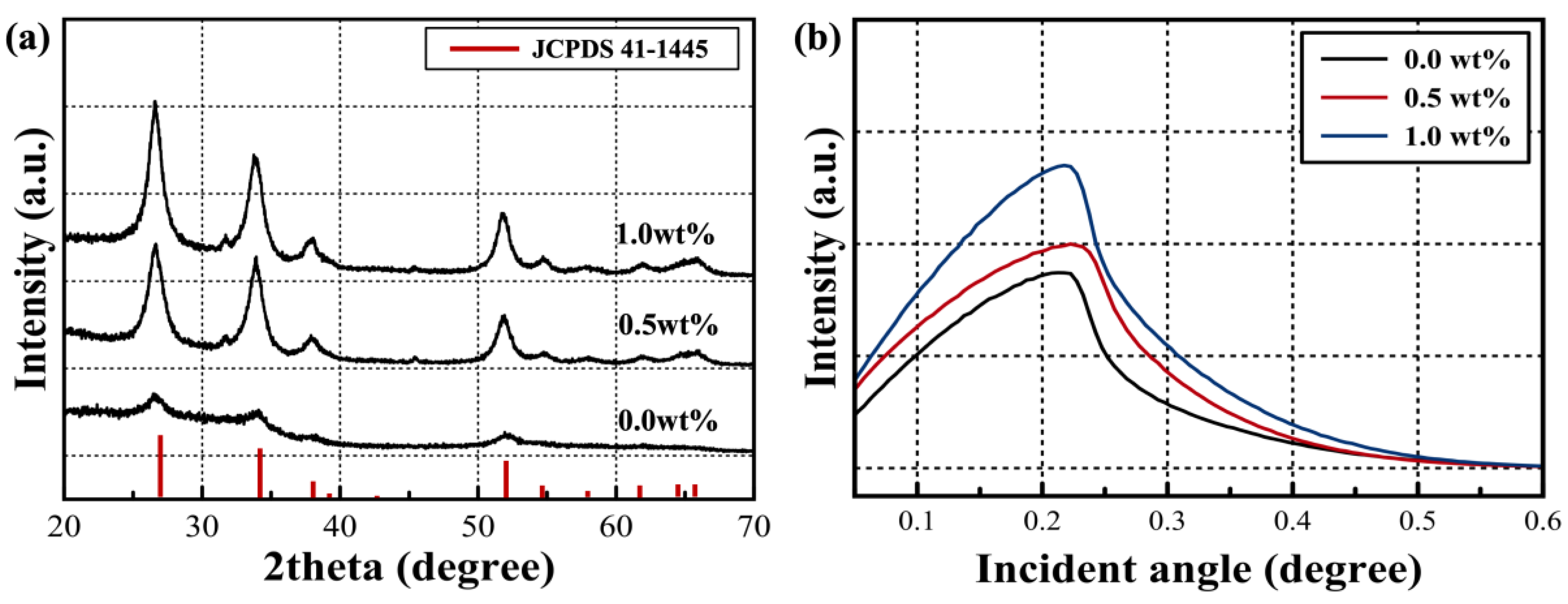
 [Green Version]
Figure 1. (a) The GIXRD spectra and (b) X-ray reflectivity curves for solution-processed SnO2 films doped with 0.0 (Pristine), 0.5 and 1.0 wt% Mg.
Electronics 09 00523 g001
Figure 2. The O 1s XPS spectra of solution-processed SnO2 films corresponding to different Mg doping concentrations. (a) 0.0 wt%, (b) 0.5 wt%, and (c) 1.0 wt%. (d)Proportions of oxygen vacancies, lattice impurities, and hydroxide impurities in Mg doped SnO2 films, determined by XPS.
Electronics 09 00523 g002
Figure 3. (a) Increased optical band gap of the solution-processed SnO2 films As the doping concentration increases. (b) Decreased valence band off set, determined by XPS spectra near the valence band. (c) Schematic energy band diagram including the relative energy position of the Fermi level with respect to the conduction band minimum and the valence band maximum.
Electronics 09 00523 g003
Figure 4. Output curves of solution-processed SnO2 TFTs with Mg doping concentration (a) 0.0 wt% (b) 0.5 wt% and (c) 1 wt% and (d) ID-VD curves of samples with 0.0 wt%, 0.5 wt%, and 1.0 wt% Mg.
Electronics 09 00523 g004aElectronics 09 00523 g004b
Figure 5. Extracted performance parameters of the fabricated Mg-doped SnO2 thin film transistors: (a) field effect mobility in the saturation regime, (b) Vth, (c) SS, and (d) Ion and Ioff.
Electronics 09 00523 g005aElectronics 09 00523 g005b
Figure 6. Transfer curves of solution-processed SnO2 TFTs depending on Mg doping concentration (a) 0.0 wt% (b) 0.5 wt% (c) 1 wt% and (d) The Vth shift under a negative bias stress.
Electronics 09 00523 g006
Figure 7. Schematic of the degradation mechanism for (a) SnO2 and (b) Mg-doped SnO2 thin film transistors (TFTs) under negative bias stress (NBS).
Electronics 09 00523 g007
Table 1. Critical angle, Film density, and Crystalline size of solution-processed SnO2 films doped with 0–1 wt% Mg.
Critical Angle (Degree)Density (g/cm3)Crystallite size (nm)
0.0 wt%0.2613.707.68
0.5 wt%0.2864.437.83
1.0 wt%0.2784.188.36

