Article

Highly Integrated Resonant Tunneling Diode with Rectangular Waveguide Output for W-Band Communication System

1
School of Electronic Engineering, Beijing University of Posts and Telecommunications, Beijing 100876, China
2
School of Electronic Engineering and Computer Science, Queen Mary, University of London, London E1 4NS, UK
*
Author to whom correspondence should be addressed.
Electronics 2020, 9(3), 485; https://doi.org/10.3390/electronics9030485
Submission received: 12 February 2020 / Revised: 1 March 2020 / Accepted: 13 March 2020 / Published: 15 March 2020
(This article belongs to the Collection Millimeter and Terahertz Wireless Communications)

Abstract

:
A packaged resonant tunneling diode (RTD) with rectangular waveguide output for highly integrated wireless communication is proposed. The output signal of the RTD chip is radiated to the rectangular waveguide through an E plane probe transformer. Next, the RTD chip is electrically connected to the transformer by using gold wire bonding. The packaged RTD exhibits an oscillation frequency of 92 GHz, while the maximum radio frequency (RF) output power is −7 dBm. A miniaturized and high data rate wireless communication system with a 7 Gbps on–off keying (OOK) module by using the RTD is demonstrated, and the bit error rate (BER) of the 7 Gbps is below 3.8 × 10⁻³.

1. Introduction

There has been an explosive growth of data capacity and data rate in fifth generation wireless networks (5G) [1]. The millimeter wave and terahertz frequency range has a large amount of unlicensed spectra, and this has gotten a lot of attention in wireless communication [2,3].
The millimeter wave and terahertz communication systems mainly include all-electronic and optoelectronic systems. The advantage of all-electronics systems is higher output power, but their data rate is lower [4,5]. Most of the optoelectronic systems are based on uni-traveling carrier photodiode (UTC-PD), which can obtain a higher data rate [6,7]. However, its system integration is poor due to its complicated optical equipment.
A resonant tunneling diode (RTD) is a high speed solid-state device [8]. Recently, many literatures on short distance and high data rate wireless communication with RTD have been published [9,10,11,12,13]. In [9], wireless data transmission by direct amplitude shift keying was demonstrated by using an RTD oscillating at 542 GHz, with a data rate of 3 Gbps. In [10], a 9 Gbps on–off keying module system was achieved, and the RTDs awee employed to be the transmitter and receiver by changing the bias voltage of the RTD. In [11], a wireless data transmission of 34 Gbit/s at 500 GHz range was proposed, where the output power was about 60 μW. To improve the RF output power, J. Park et al. designed an RTD pair configuration to obtain an increased negative differential conductance voltage span; the maximum RF output power was −1.76 dBm at 24.1 GHz [12]. In the same year, J. Wang et al. also proposed an improved RTD pair, and the maximum output power was 2 mW without any power amplifier at the oscillator frequency 84 GHz [13].
However, the use of a probe station and DC bias lines reduce the flexibility of RTD chips, and the exposed RTD chips are susceptible to mechanical damage, which makes them difficult to apply in the communication system. In addition, to the best of our knowledge, there has been no literature on a packaged RTD due to the complicated packaged process, including DC bias, electrical signal connection, and efficient RF conversion.
Most millimeter wave and terahertz devices are waveguide output. To enhance system integrity, it is necessary to package the RTD with a rectangular waveguide output. In this paper, an RTD with rectangular waveguide output for a W band communication system application is presented. First, a coplanar waveguide (CPW) transition to rectangular waveguide structure based on the E plane probe was designed to achieve the output signal of the RTD efficiently coupled into rectangular waveguide. Then, we designed the packaged RTD structure, and we fabricated and measured the performance of the packaged RTD. Measured results demonstrated that the oscillation frequency of the packaged RTD was from 88 to 92 GHz, and the maximum RF output power was −7 dBm. Finally, to verify the wireless transmission capability of the packaged RTD, a highly integrated and high speed wireless communication system based on on–off keying (OOK) modulation with the RTD was built, and the date rate of 7 Gbps was realized.

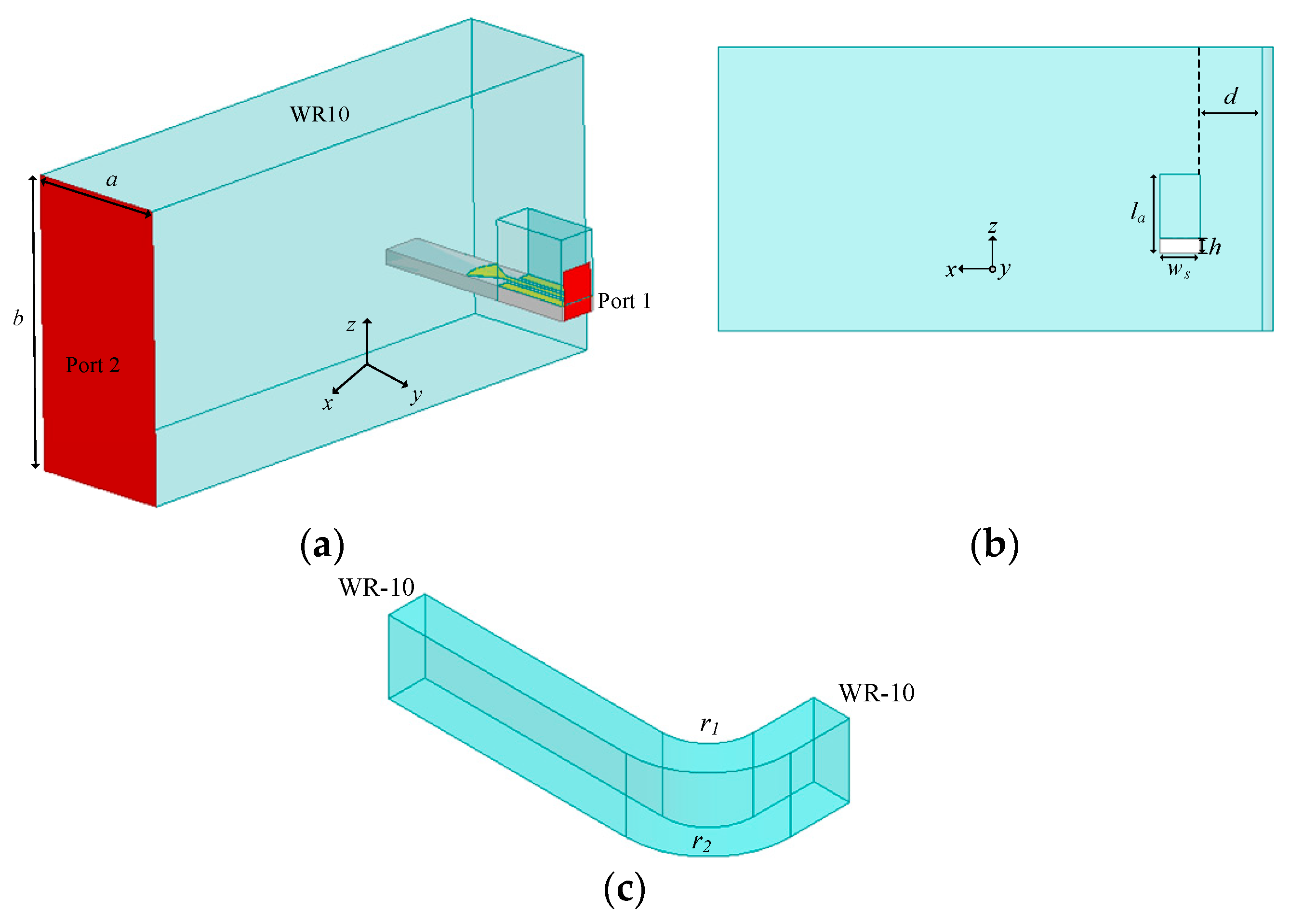
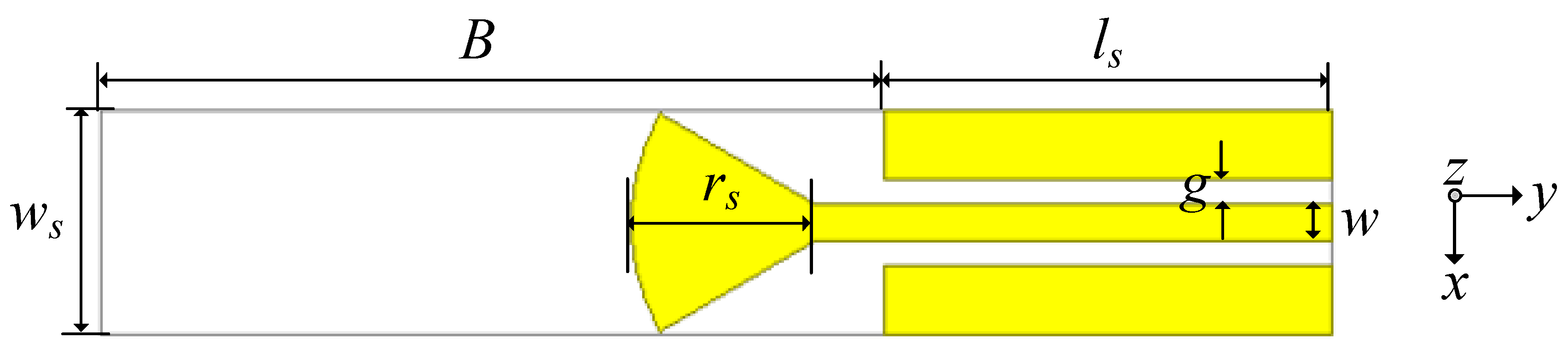
2. CPW—Waveguide Transformer Design

2.1. Transformer Structure Design

Figure 1 shows the structure of CPW transition to waveguide. The rectangular waveguide was a standard WR-10 waveguide, and a window connecting to the air cavity was opened in parallel with the H plane of the waveguide. The length of the window was the same as the CPW length, and the width and height of the window were ws and la, respectively. One end of the rectangular waveguide was blocked with solid metal block. An H plane bend structure was designed to facilitate the measure, and the bending radii were r1 and r2, as shown in Figure 1c. The fan-shaped radiation part connected to the end of the signal trace of the CPW was used to propagate the wave of the CPW into the waveguide, as shown in Figure 2. The E plane probe was designed on the high permittivity Al2O3 substrate. The relative permittivity was 9.8, and the height was 127 μm. The numerical analysis software Ansoft HFSS (High Frequency Structure Simulator) was used to simulate the configuration. The red parts in the Figure 1a are the wave ports, and the optimized detailed parameters of the transformer are shown in Table 1.

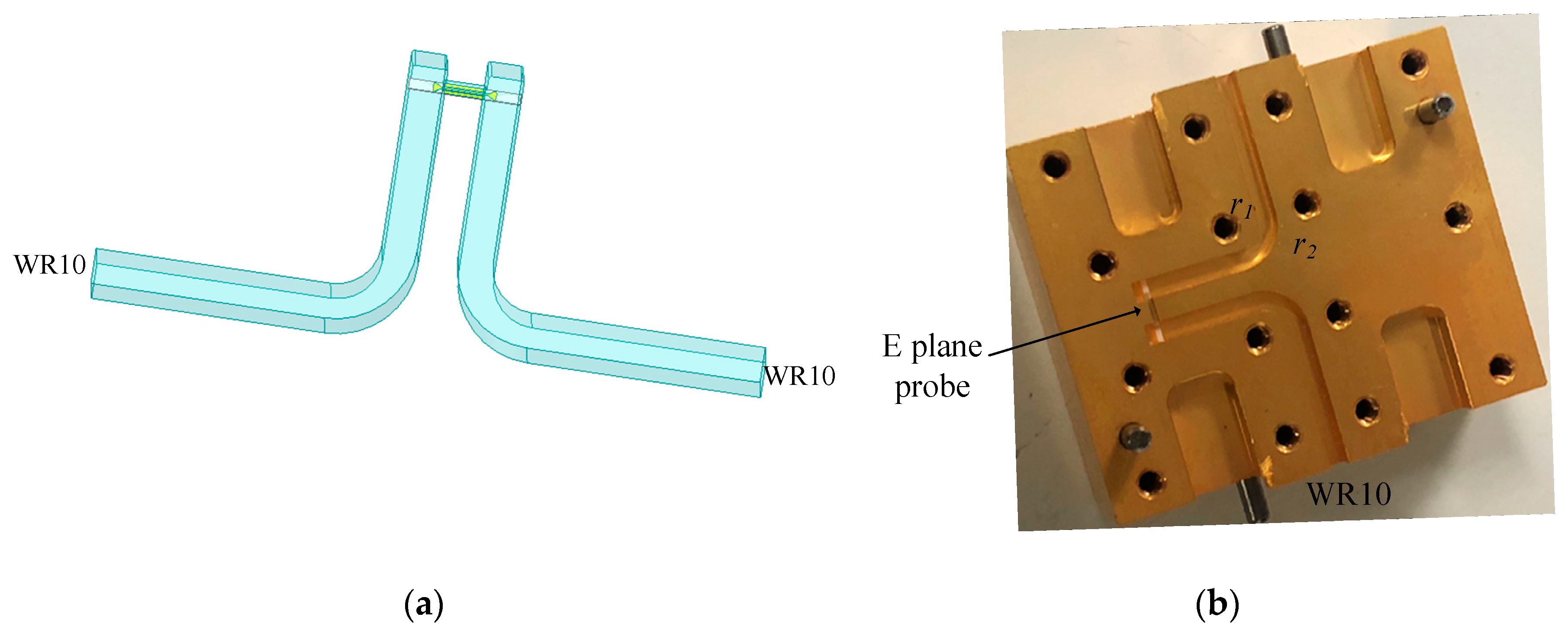
2.2. Simulated and Measured Results

In order to measure the E plane probe transformer performance, it was necessary to design a back to back structure. Figure 3a shows the simulated configuration, and the fabricated photograph is shown in Figure 3b. The gold plated E plane probe was designed on the Al2O3 substrate with thin film circuit technology, and the thickness of the gold was about 0.5 μm. The copper plated with a gold waveguide was fabricated by a milling and discharging process, and a 127 μm-deep slot was etched in the lower plane of waveguide. The E plane probe transformer was put in the slot with silver conductive glue. The S-parameters of the transition were measured by using a vector network analyzer (VNA) with WR10 frequency extenders. Figure 4 shows the simulated and measured S-parameters of the transition. By mainly optimizing the window position d and the fan-shaped radiation length rs, the transformer could obtain a good performance. The measured results verified that the transition had a wider impedance bandwidth of 38% for |S11|< −10 dB, and the insertion loss was, on average, 1.2 dB. The discrepancy between the simulated and measured results was mainly due to the machining and assembly errors.

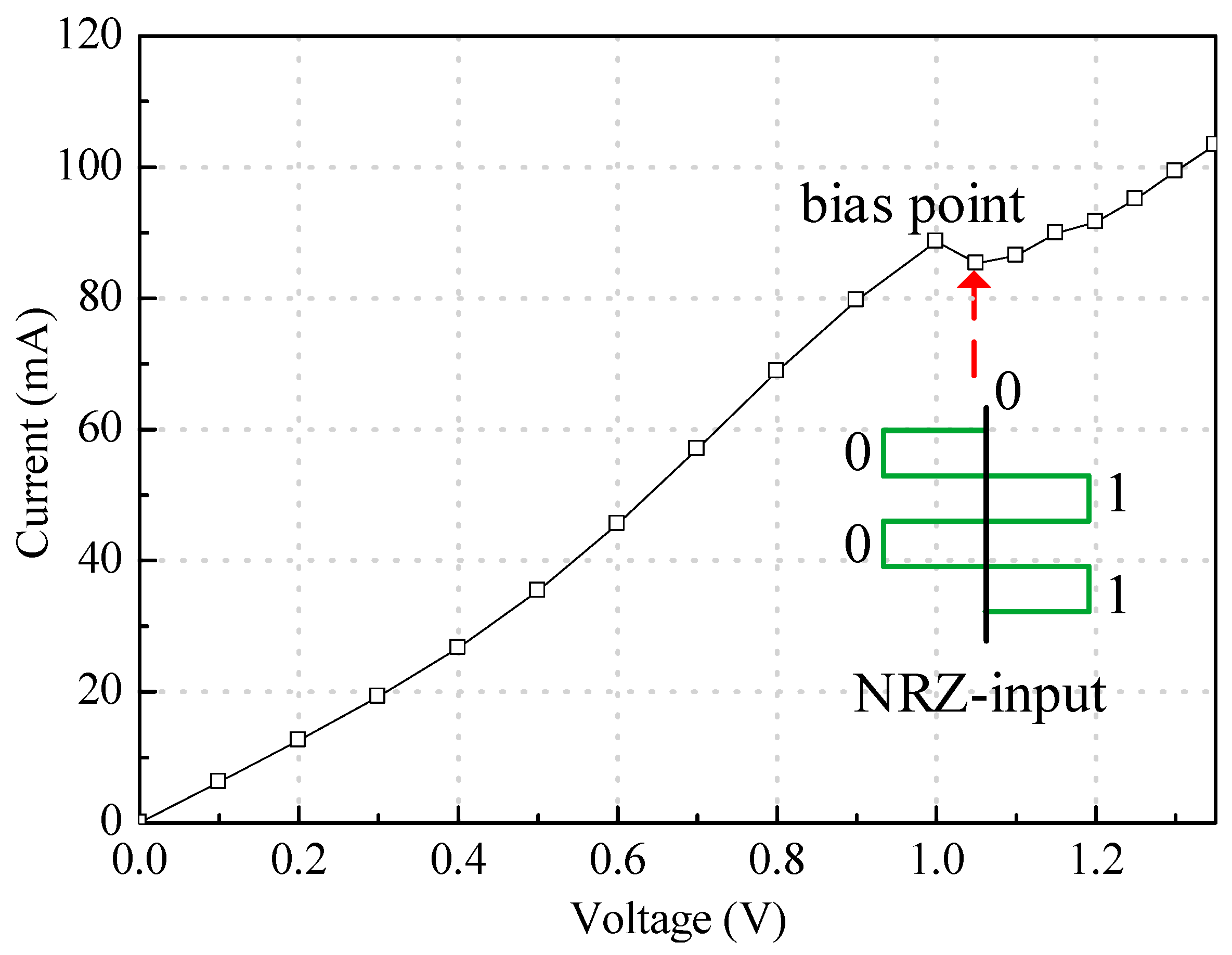
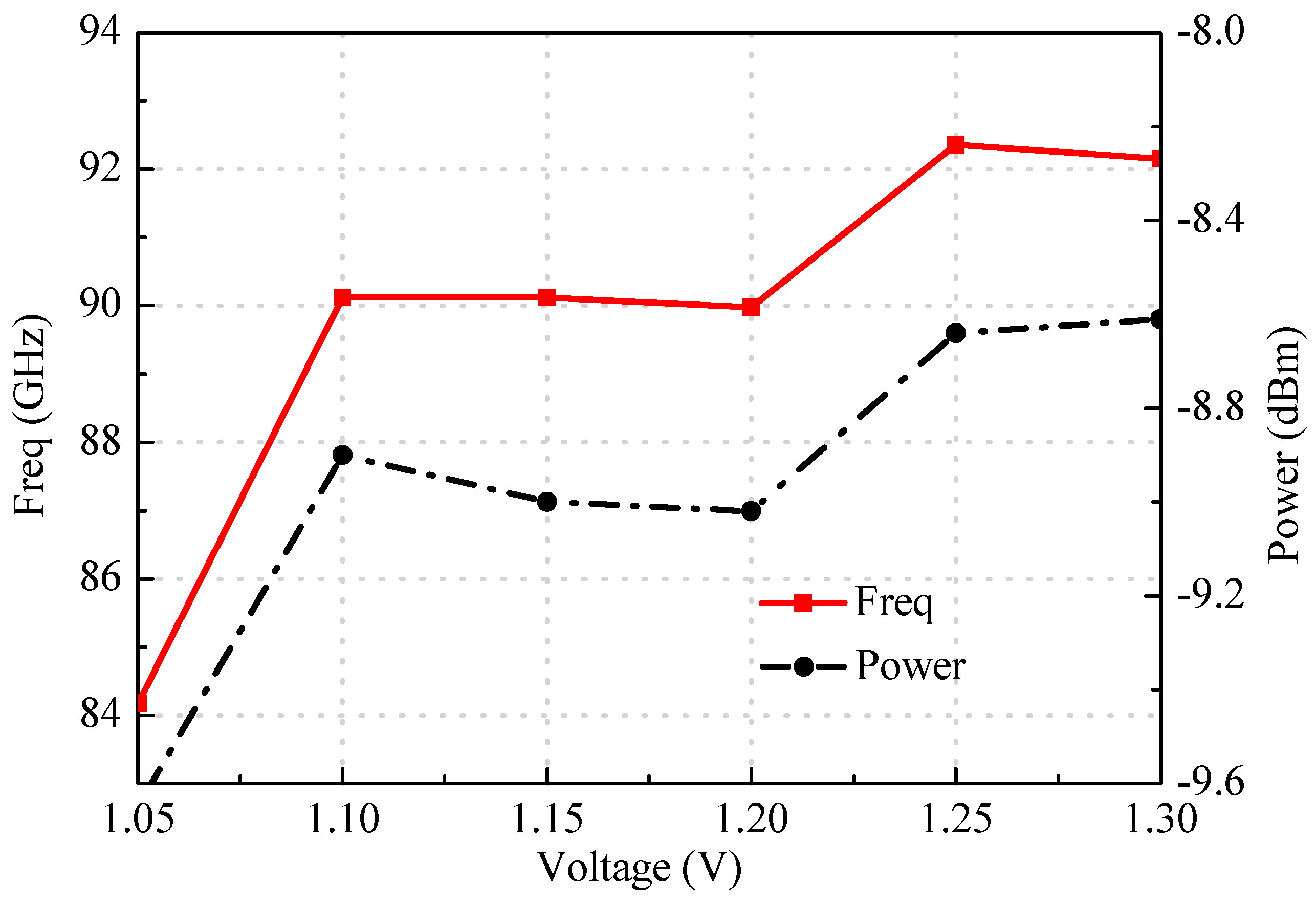
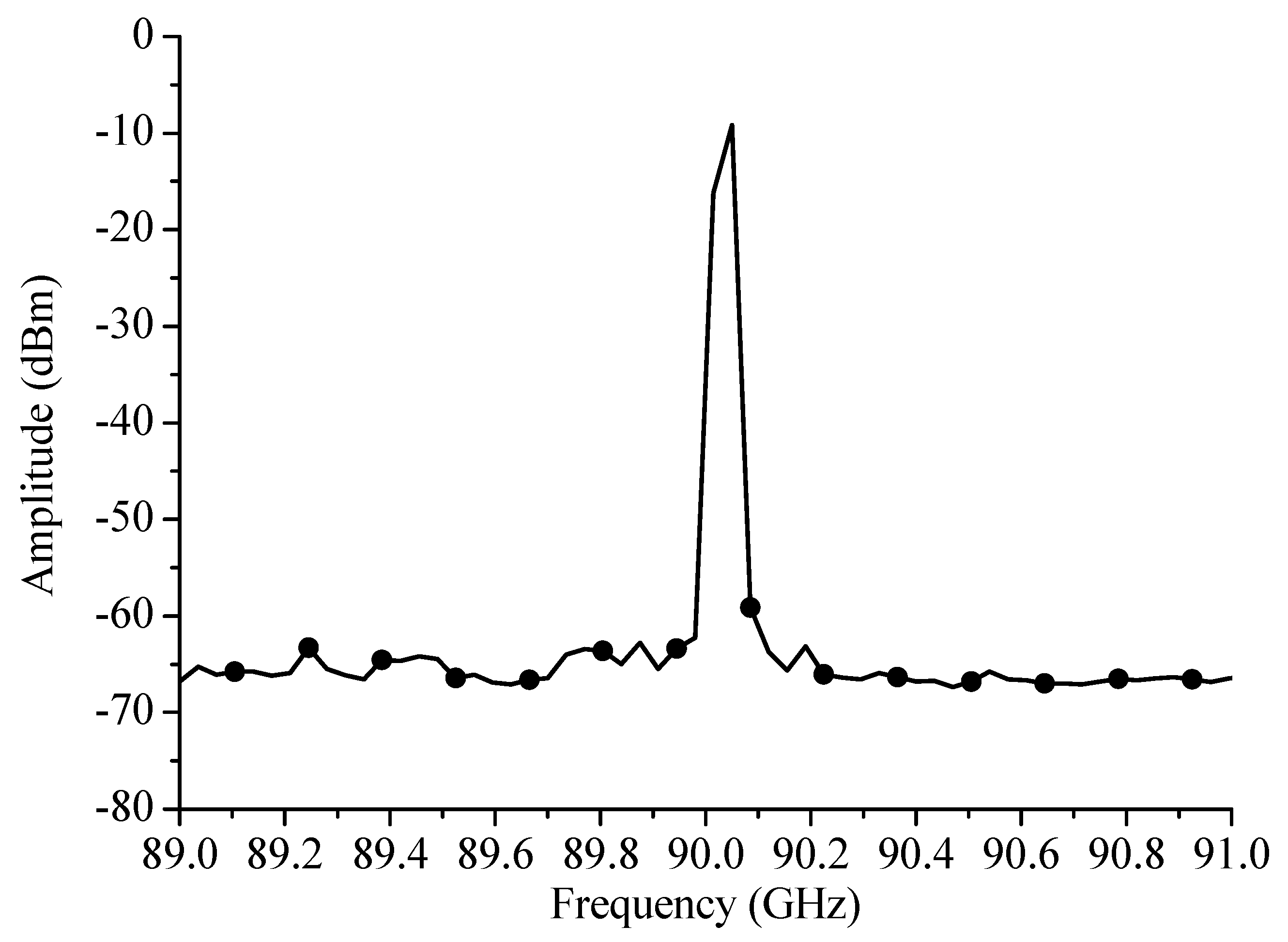
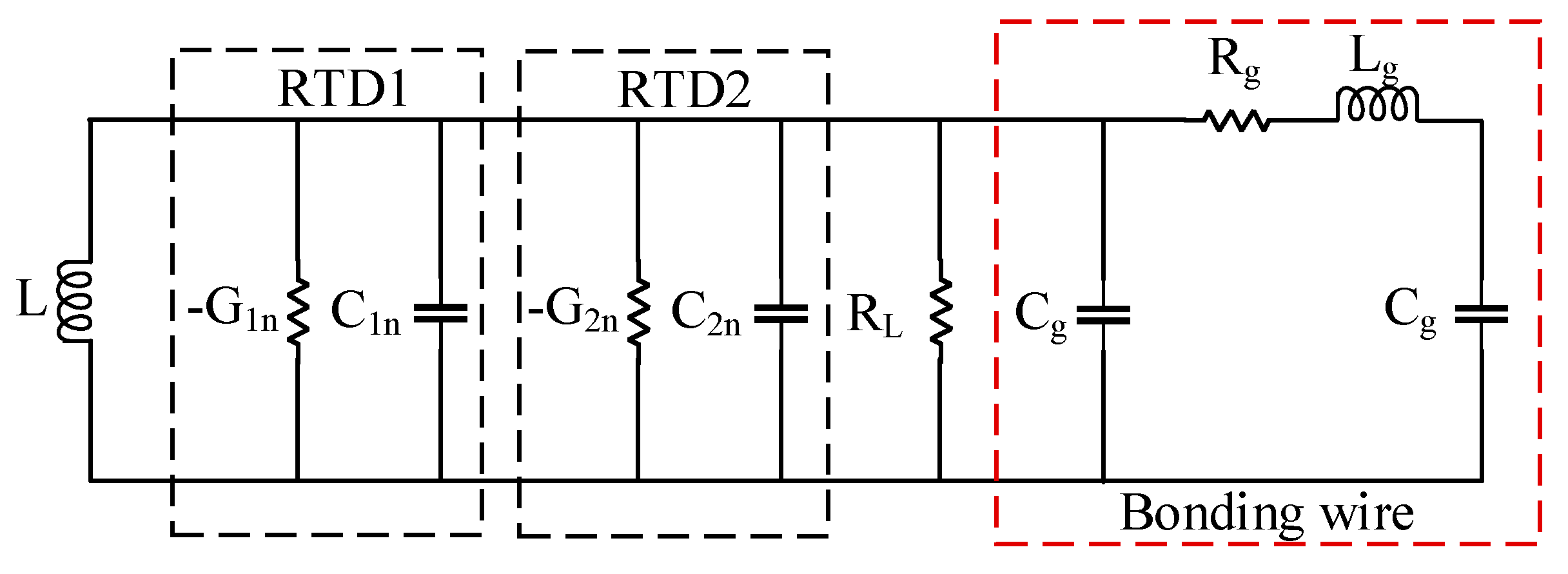
3. Package and Measurement of RTD

The packaged RTD configuration with WR10 waveguide output and an SMA connector is shown in Figure 5. The packaged RTD consisted of a DC bias microstrip line (MSL), an RTD chip, an E plane probe transformer, and a metallic cavity with WR 10 waveguide output. The DC bias MSL that was connected to an SMA connector was used to bias the RTD. The MSL was designed on the Rogers 6010 substrate with a relative permittivity of 10.2 and a thickness of 127 μm. The width of the MSL was 0.1 mm to match with the 50 Ω SMA connector. The RTD chip was the same as in the one used in the literature [14], and the indium phosphide (InP) substrate height of the RTD was 600 μm. The E plane probe transformer was used to radiate the RF signal of the RTD to the WR 10 waveguide. By using gold wire bonding, the signal and ground traces of the RTD were connected to the E plane probe transformer and the DC MSL was bonded to the DC trace of the RTD. A metallic package cavity with a WR-10 standard waveguide output was fabricated. We etched three slots in the cavity and used a conductive silver glue to fix the transformer, the RTD chip, and the DC bias MSL inside the cavity. The photograph and micrograph of the fabricated packaged RTD is shown in Figure 6.
Figure 7 shows the I–V characteristics of the packaged RTD. The RTD chip in the literature [14] consists of two RTDs that are connected in parallel, and each device is biased individually with resistor Re. Because of the additional current through the shunt resistor that is connected in parallel with the RTD, a negative differential resistance (NDR) region was not observed in the I–V curve [13]. Instead, a small decline of 1.05 V was observed, and 1.05 V was the bias point of the RTD. As proposed in [14], by changing the DC voltage, an RTD can operate in negative differential resistance region or positive resistance region. Therefore, an RTD can be biased to switch between the on and off states with OOK modulation. The voltage-dependent frequency and output power of RTD is shown in Figure 8. The oscillator frequency ranged from 88 to 92 GHz, and the maximum RF output power was −8.6 dBm. When the losses of the cable, the SMA adapters, and the bias-T were removed, the actual output power was at least −7 dBm. Figure 9 shows the output spectrum at 90 GHz when DC = 1.2 V.
The carrier frequency of the RTD with a waveguide output increased by 15 GHz compared with the RTD chip, an effect that was mainly caused by gold wire bonding. The packaged RTD equivalent circuit, including gold wire bonding, is shown in Figure 10. The RTD oscillator circuit part was the same as [15], and −G1n and −G2n were the negative differential conductances of RTD1 and RTD2, respectively, while C1n and C2n were the self-capacitances of each RTD. The gold wire was equivalent to series inductance and parallel capacitance. Generally, the effect of shunt capacitors is negligible due to their smaller value. Oscillator frequency can be determined by equating the admittance imaginary part to zero, as shown in Equation (1):
f = 1 2 π ( C 1 n + C 1 n ) L L g L + L g
where Lg is the series inductance of gold wire. It can be seen that the total inductance in the circuit was decreased compared with that of [15], which led to the increased carrier frequency.
Figure 11 shows the output spectrum with OOK modulation at 90 GHz when DC = 1.2 V. The modulation signal was a pseudorandom bit sequence (PRBS) with repetition length 215–1, and the data rate was 4 Gbps. The first null appeared at 94 GHz, which verified the feasibility of the packaged RTD for OOK modulation.

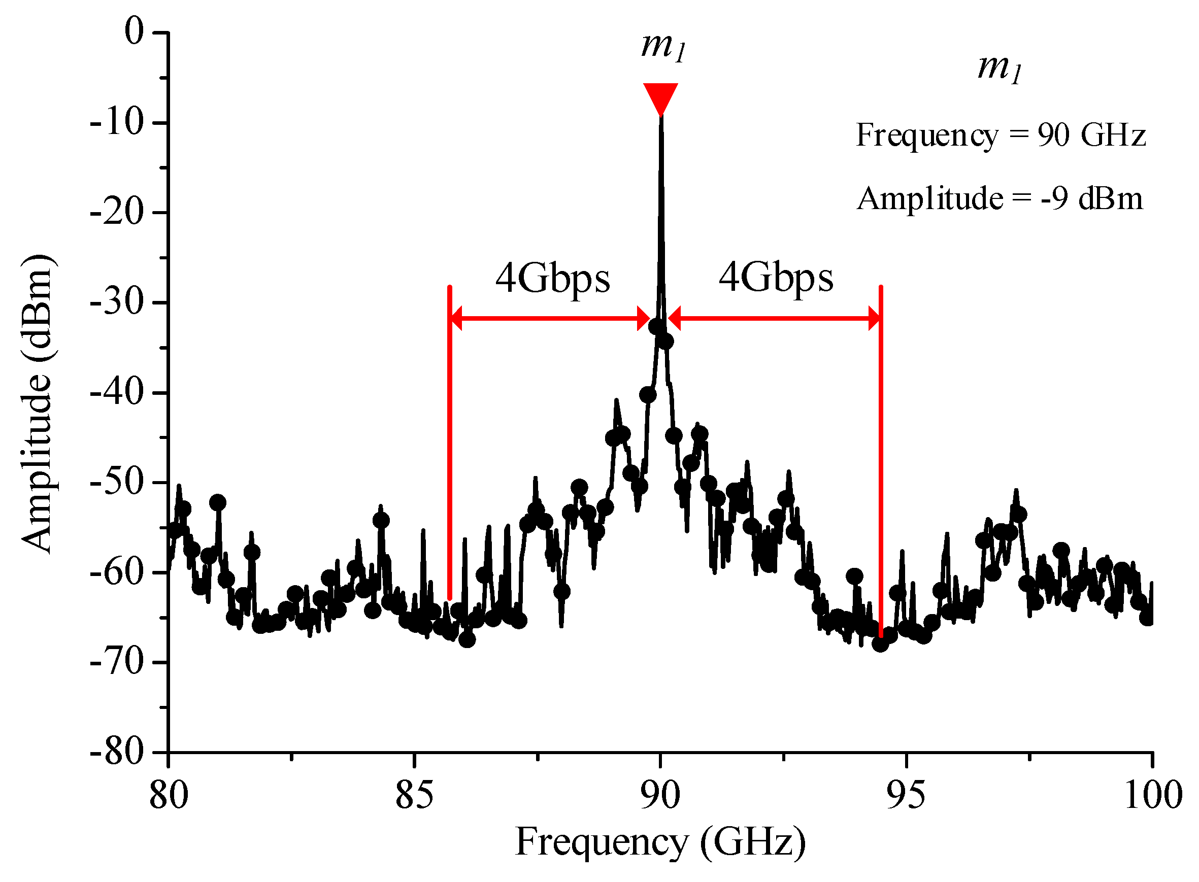
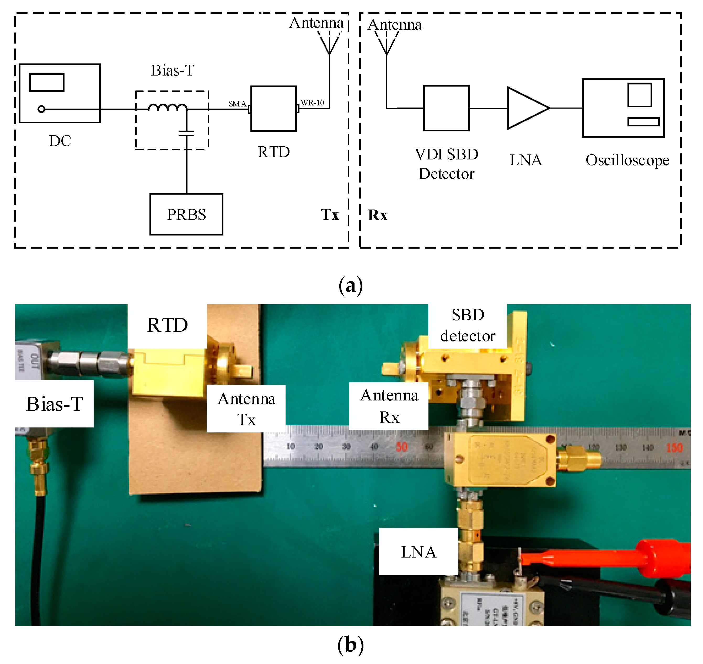
4. System Demonstration

The highly integrated wireless communication system is shown in Figure 12. The RTD was the transmitter, and bias-T was used for applying DC and PRBS signals to the RTD. Two waveguide antennas with a gain of 10 dBic were employed to transmit and receive signals. The data were demodulated by a zero bias VDI SBD detector, and then they were amplified by a low noise amplifier (LNA). The bias voltage was 1.2 V instead of 1.05 V due to the loss of the bias-T, and the amplitude of PRBS signal ranged from −100 to 100 mV. It can be seen from Figure 7 that 1.05 + 0.1 V was in the NDR (on state), while 1.05 − 0.1 V was in the positive resistance region (off state). The transmission distance was 5 cm, and the maximum data rate was 8 Gbps. The bit error rate and eye diagram are shown in Figure 13. The BER was below 3.8 × 10⁻³ up to 7 Gbps.
Finally, Table 2 lists the performance of the reported wireless communication systems that use RTD. The oscillator frequencies were higher in [9,10,11]. Compared with the system in [9], the proposed RTD had a higher data rate, and the proposed RTD had a higher output power than the RTD in [11]. Though the output power was higher in [12], the oscillator frequency was 24 GHz, which is difficult to use for millimeter wave and terahertz application. The RTD chip proposed in the literature [14] had a higher output power and data rate, and this was the chip that was used in our packaged RTD. However, the RTD chips mentioned in these documents are difficult to use in practical communication systems. The proposed packaged RTD biased the RTD through the SMA connector, and the output was a standard waveguide that could easily connect to a waveguide device, thus achieving system miniaturization and effectively improving system integration.

5. Conclusions

This paper presented a highly integrated resonant tunneling diode (RTD) with a rectangular waveguide output for W band wireless communication systems. The RTD carrier frequency was 92 GHz, and the maximum RF output power was −7 dBm at a bias voltage of 1.25 V. The effect of the gold wire bonding on the oscillation frequency was also analyzed. In addition, short distance and high data rate transmission could be realized by using the packaged RTD, and the system integration was significantly improved. The results showed that the RTD has the potential for millimeter wave and terahertz wireless communication and imaging.

Author Contributions

Formal analysis, C.W.; validation, C.W., Y.Y., J.Y. and X.C.; formal analysis, C.W.; investigation, H.J. and T.X.; resources, J.Y.; data curation, C.W.; writing—original draft preparation, C.W.; writing—review and editing, J.Y., M.A.S.S. and X.C.; supervision, Y.Y. and X.C.; project administration, Y.Y.; funding acquisition, Y.Y. All authors have read and agreed to the published version of the manuscript.

Funding

This work was funded by Nation Natural Science Foundation of China under grant 61474112.

Acknowledgments

The authors would like to thank Edward Wasige and Jue Wang from the High Frequency Electronics Group, University of Glasgow, for providing us with RTD chip, as well as their valuable help with the system measurement.

Conflicts of Interest

The authors declare that there is no conflict of interests regarding the publication of this article.

References

  1. Yu, X.; Asif, R.; Piels, M.; Zibar, D.; Galili, M.; Morioka, T.; Jepsen, P.U. 400-GHz wireless transmission of 60-Gb/s Nyquist-QPSK signals using UTC-PD and heterodyne mixer. IEEE Trans. Terahertz Sci. Technol. 2016, 6, 765–770. [Google Scholar] [CrossRef] [Green Version]
  2. Jia, S.; Pang, X.; Ozolins, O.; Yu, X.; Hu, H.; Yu, J.; Guan, P.; Da Ros, F.; Popov, S.; Jacobsen, G.; et al. 0.4 THz photonic-wireless link with 106 Gb/s single channel bitrate. J. Lightwave Technol. 2018, 36, 610–616. [Google Scholar] [CrossRef] [Green Version]
  3. Koenig, S.; Lopez-Diaz, D.; Antes, J. Wireless sub-THz communication system with high data rate. Nat. Photonics 2013, 7, 977–981. [Google Scholar] [CrossRef]
  4. Wu, Q.; Lin, C.; Lu, B.; Miao, L.; Hao, X.; Wang, Z.; Jiang, Y.; Lei, W.; Den, X.; Chen, H.; et al. A 21 km 5 Gbps real time wireless communication system at 0.14 THz. In Proceedings of the International Conference on Infrared, Millimeter, and Terahertz Waves, Cancun, Quintana Roo, Mexico, 27 August–1 September 2017. [Google Scholar]
  5. Wang, C.; Lu, B.; Lin, C.; Chen, Q.; Miao, L.; Deng, X.; Zhang, J. 0.34-THz wireless link based on high-order modulation for future wireless local area network applications. IEEE Trans. Terahertz Sci. Technol. 2014, 1, 75–85. [Google Scholar] [CrossRef]
  6. Li, X.; Yu, J.; Wang, K. Delivery of 54-Gbps 8QAM W-Band signal and 32-Gbps 16QAM K-Band signal over 20-km SMF-28 and 2500-m wireless distance. J. Lightwave Technol. 2017, 36, 610–616. [Google Scholar]
  7. Li, X.; Yu, J.; Zhao, L.; Wang, K.; Wang, C.; Zhao, M.; Zhou, W.; Xiao, J. 1-Tb/s Millimeter-Wave Signal Wireless Delivery at D-Band. J. Lightwave Technol. 2019, 37, 196–203. [Google Scholar] [CrossRef]
  8. Webber, J.; Nishigami, N.; Kim, J.-Y. Terahertz wireless communications using resonant tunnelling diodes with radio-over-fibre. Electron. Lett. 2019, 55, 949–951. [Google Scholar] [CrossRef]
  9. Ishigaki, K.; Shiraishi, M.; Suzuki, S. Direct intensity modulation and wireless data transmission characteristics of terahertz-oscillating resonant tunnelling diodes. Electron. Lett. 2012, 48, 582–583. [Google Scholar] [CrossRef]
  10. Diebold, S.; Nishio, K.; Nishida, Y. High-speed error-free wireless data transmission using a terahertz resonant tunnelling diode transmitter and receiver. Electron. Lett. 2016, 52, 1999–2001. [Google Scholar] [CrossRef]
  11. Oshima, N.; Hashimoto, K.; Suzuki, S. Wireless data transmission of 34 Gbit/s at a 500-GHz range using resonant-tunnelling-diode terahertz oscillator. Electron. Lett. 2016, 52, 1897–1898. [Google Scholar] [CrossRef]
  12. Park, J.; Lee, J.; Yang, K. A 24-GHz low-power RTD-based on–ogg keying oscillator with a RTD pair configuration. IEEE Microw. Wirel. Compon. Lett. 2018, 28, 521–523. [Google Scholar] [CrossRef]
  13. Oshima, N.; Hashimoto, K.; Suzuki, S.; Asada, M. Terahertz wireless data transmission with frequency and polarization division multiplexing using resonant-tunneling-diode oscillators. IEEE Trans. Terahertz Sci. Technol. 2017, 7, 593–598. [Google Scholar] [CrossRef]
  14. Wang, J.; Al-Khalidi, A.; Wang, L.Q.; Morariu, R. 15-Gb/s 50-cm wireless link using a high-power compact III–V 84-GHz transmitter. IEEE Trans. Microw. Theory Tech. 2018, 66, 4698–4705. [Google Scholar]
  15. Wang, J.; Wang, L.; Li, C. 28 GHz MMIC resonant tunnelling diode oscillator of around 1mW output power. Electron. Lett. 2013, 49, 816–818. [Google Scholar] [CrossRef] [Green Version]
Figure 1. The configuration of the transformer. (a) 3D view; (b) side view; and (c) H plane bend.
Electronics 09 00485 g001
Figure 2. The configuration of the E plane probe.
Electronics 09 00485 g002
Figure 3. Back-to-back photograph of the transition. (a) Simulated configuration; (b) fabricated photograph (the upper layer is hidden).
Electronics 09 00485 g003
Figure 4. Simulated and measured S-parameters of the transition.
Electronics 09 00485 g004
Figure 5. The packaged resonant tunneling diode (RTD) configuration.
Electronics 09 00485 g005
Figure 6. Photograph and micrograph of the RTD with a rectangular waveguide output.
Electronics 09 00485 g006
Figure 7. The I–V characteristics of the packaged RTD.
Electronics 09 00485 g007
Figure 8. Measured voltage-dependent frequency and output power of the RTD.
Electronics 09 00485 g008
Figure 9. Measured output spectrum of the RTD oscillator.
Electronics 09 00485 g009
Figure 10. Packaged RTD equivalent circuit including gold wire bonding.
Electronics 09 00485 g010
Figure 11. Measured output spectrum of RTD with OOK modulation.
Electronics 09 00485 g011
Figure 12. High-integrated wireless communication system. (a) Block diagram; (b) Photograph.
Electronics 09 00485 g012
Figure 13. Measured bit error rate (BER) and eye diagram of RTD oscillator.
Electronics 09 00485 g013
Table 1. Geometrical parameters of the transformer.
ParameterABlswsrsla
value (mm)2.541.270.730.360.30.7
parameterdwghr1r2
value (mm)0.660.060.040.1271.62.9
Table 2. Performance of the proposed RTD.
Ref.Oscillator Frequency (GHz)Output Power (dBm)Data Rate
(Gbps)
RTD
[9]542−6.73chip
[10]286N.A.9chip
[11]500−12.234chip
[12]24−1.765Chip
[14]84315Chip
Proposed92−77packaged

