Article

Electrical Performance and Stability Improvements of High-Mobility Indium–Gallium–Tin Oxide Thin-Film Transistors Using an Oxidized Aluminum Capping Layer of Optimal Thickness

School of Electrical and Electronics Engineering, Chung-Ang University, Seoul 06972, Korea
*
Author to whom correspondence should be addressed.
Electronics 2020, 9(12), 2196; https://doi.org/10.3390/electronics9122196
Submission received: 21 November 2020 / Revised: 10 December 2020 / Accepted: 17 December 2020 / Published: 20 December 2020
(This article belongs to the Special Issue Applications of Thin Films in Microelectronics)

Abstract

:
We examined the effects of aluminum (Al) capping layer thickness on the electrical performance and stability of high-mobility indium–gallium–tin oxide (IGTO) thin-film transistors (TFTs). The Al capping layers with thicknesses (tAls) of 3, 5, and 8 nm were deposited, respectively, on top of the IGTO thin film by electron beam evaporation, and the IGTO TFTs without and with Al capping layers were subjected to thermal annealing at 200 °C for 1 h in ambient air. Among the IGTO TFTs without and with Al capping layers, the TFT with a 3 nm thick Al capping layer exhibited excellent electrical performance (field-effect mobility: 26.4 cm2/V s, subthreshold swing: 0.20 V/dec, and threshold voltage: −1.7 V) and higher electrical stability under positive and negative bias illumination stresses than other TFTs. To elucidate the physical mechanism responsible for the observed phenomenon, we compared the O1s spectra of the IGTO thin films without and with Al capping layers using X-ray photoelectron spectroscopy analyses. From the characterization results, it was observed that the weakly bonded oxygen-related components decreased from 25.0 to 10.0%, whereas the oxygen-deficient portion was maintained at 24.4% after the formation of the 3 nm thick Al capping layer. In contrast, a significant increase in the oxygen-deficient portion was observed after the formation of the Al capping layers having tAl values greater than 3 nm. These results imply that the thicker Al capping layer has a stronger gathering power for the oxygen species, and that 3 nm is the optimum thickness of the Al capping layer, which can selectively remove the weakly bonded oxygen species acting as subgap tail states within the IGTO. The results of this study thus demonstrate that the formation of an Al capping layer with the optimal thickness is a practical and useful method to enhance the electrical performance and stability of high-mobility IGTO TFTs.

1. Introduction

Amorphous oxide semiconductor (AOS) thin-film transistors (TFTs) are of significant interest for applications in active matrix displays, sensors, memories, and other electronic systems because of their excellent electrical properties, good uniformities, and low fabrication costs [1,2,3,4]. Among them, the indium–gallium–zinc oxide (IGZO) TFT, which was first introduced by Nomura et al., in 2004 [5], is the most popular AOS TFT that is currently used for commercial products such as large-area active matrix organic light-emitting diode televisions. However, the field-effect mobility (μFE = ~10 cm2/V s) of the IGZO TFT is insufficient to meet the requirements of large area, high-frame rate, and ultra-high-resolution next-generation displays [6,7,8]. Furthermore, μFE of the TFT should be higher than that of the IGZO TFT to integrate the scan/driver circuits composed of the TFTs into a glass or flexible substrate. To date, a variety of AOS TFTs having higher μFE values than those of the IGZO TFTs have been intensively studied for application in next-generation displays [9,10,11]. Among them, the indium–gallium–tin oxide (IGTO) TFT has recently been attracting special attention as a promising high-mobility AOS TFT, because it exhibits excellent electrical properties even at low annealing temperatures (<200 °C) [12,13,14]. Low temperature processing is exceedingly important for flexible display applications because most plastic substrates have low glass transition temperatures (below 200 °C) [15,16]. In IGTO, the cation Sn is used instead of Zn, because a similar electronic configuration of Sn4+ and In3+ can increase the electron mobility within the AOS by facilitating percolation path formation [17,18,19].
To date, several previous studies have investigated the effects of metal capping layers on the electrical characteristics of AOS TFTs [20,21,22]. Ji et al. examined the effects of titanium (Ti) capping layer formation and subsequent thermal annealing on the electrical properties of indium–zinc oxide (IZO) TFTs [23]. They showed that the Ti capping layer could enhance the μFE and positive bias stress (PBS) stability of IZO TFTs. Kim et al. compared the transfer characteristics of zinc oxynitride (ZnON) TFTs with and without the tantalum (Ta) capping layer and observed that the Ta capping layer could increase μFE of the ZnON TFTs [24]. Recently, Park et al. showed that the aluminum (Al) capping layer could enhance μFE of IGZO TFTs even without the subsequent post-deposition thermal annealing process [25]. However, there has been no study on the optimal thickness of the metal capping layer for AOS TFTs considering both the electrical performance and stability of the devices. In this study, we investigated the effects of Al capping layer thickness (tAl) on the electrical characteristics, PBS stability, and negative bias illumination stress (NBIS) stability of high-mobility IGTO TFTs. Al capping layers with tAl values of 3, 5, and 8 nm were deposited on top of the IGTO thin films using the electron beam evaporation technique and the IGTO TFTs without and with Al capping layers were thermally annealed at 200 °C for 1 h in ambient air. From the experimental results, it was concluded that the 3 nm thick Al capping layer was most advantageous for improving the electrical performance and stability of IGTO TFTs. A systematic study was performed to analyze the effects of the Al capping layer with each thickness on the electrical characteristics and stabilities of IGTO TFTs.

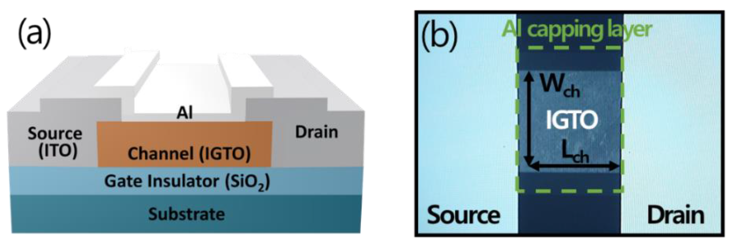
2. Experimental Details

The IGTO TFTs were fabricated on a heavily doped p-type silicon wafer (resistivity < 0.005 Ω cm) covered by 100 nm thick thermally grown SiO2 with the bottom-gate configuration. A 15 nm thick IGTO thin film was deposited via direct current (DC) magnetron sputtering using a 3 inch IGTO target. The working pressure and Ar/O2 ratio were maintained at 3 mTorr and 35/15 (sccm/sccm), respectively, during the deposition process. The DC power was fixed at 150 W, and the substrate was not intentionally heated. A 100 nm thick indium–tin oxide (ITO) was deposited on the IGTO/SiO2/Si by DC magnetron sputtering for the source and drain electrodes of the TFTs. During the sputtering of the ITO, the DC power was fixed at 150 W and the working pressure was maintained at 3 mTorr under an Ar atmosphere. Subsequently, Al capping layers with tAl values of 3, 5, and 8 nm were deposited on top of the IGTO channel layer by electron beam evaporation, respectively. Finally, the fabricated IGTO TFTs without and with Al capping layers were thermally annealed at 200 °C for 1 h in ambient air. All layers were patterned using photolithography and lift-off processes. Figure 1a and b display the schematic view and optical image of the fabricated Al-capped IGTO TFTs, respectively. All IGTO TFTs in this study were designed to have a channel width/length (W/L) of 500/500 (μm/μm). The chemical compositions of the IGTO thin films covered by Al capping layers of different thicknesses were examined by X-ray photoelectron spectroscopy (XPS, K-alpha+, Thermo Scientific). The work-function (Φ) of the deposited IGTO thin film was determined by Kelvin probe force microscopy (SKP5050, KP Technology), and the optical bandgap (Eg) of the IGTO thin film was calculated via ultraviolet visible-near infrared (UV-vis-NIR, wavelength: 300–1400 nm) spectroscopy (V-670, JASCO) using a Tauc plot. The electrical characteristics of the IGTO TFTs were measured using a semiconductor parameter analyzer (4156C, Agilent Technologies) in the dark at room temperature in a vacuum environment to avoid environmental ambient effects on the electrical characteristics and stabilities of the IGTO TFTs.

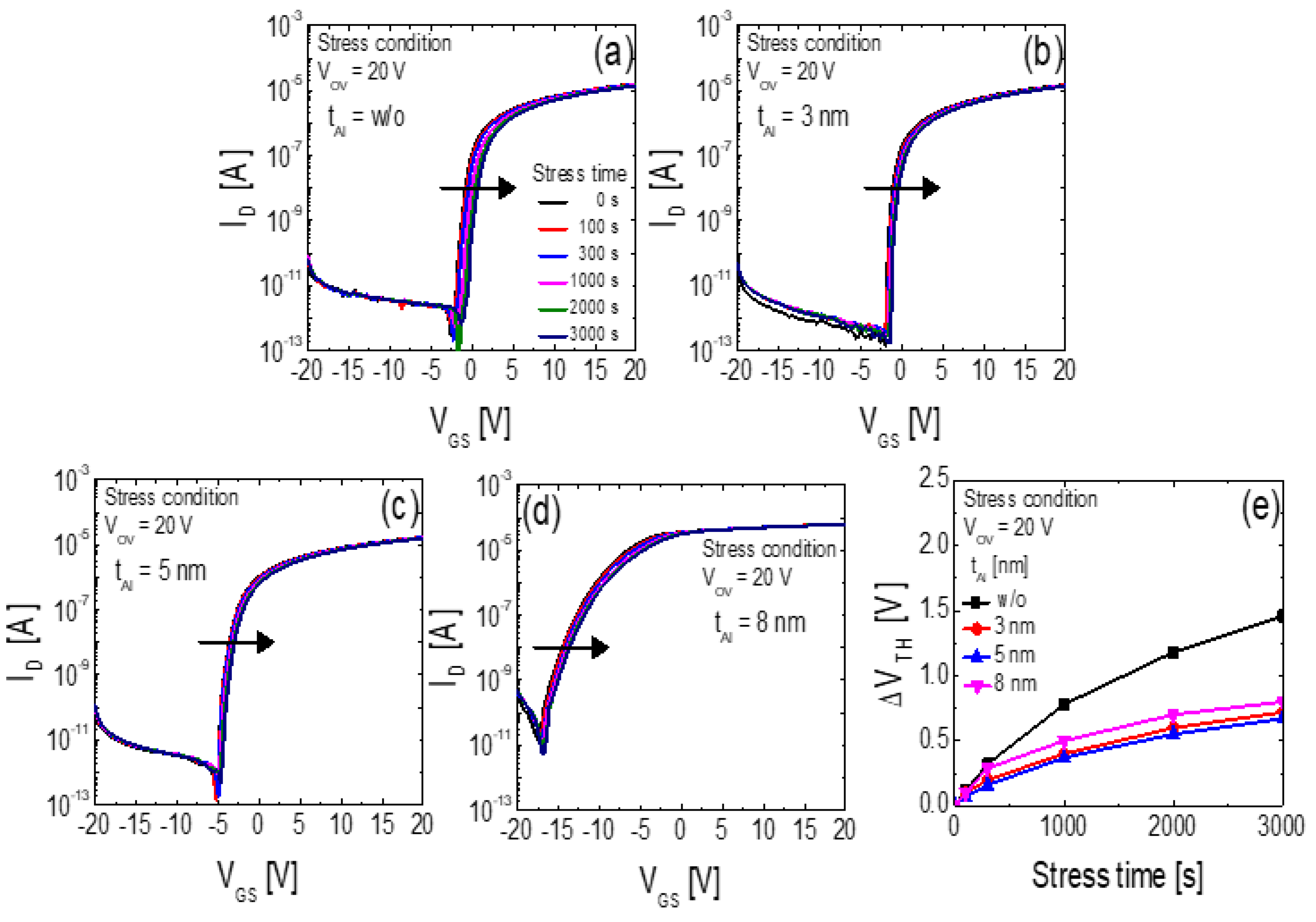
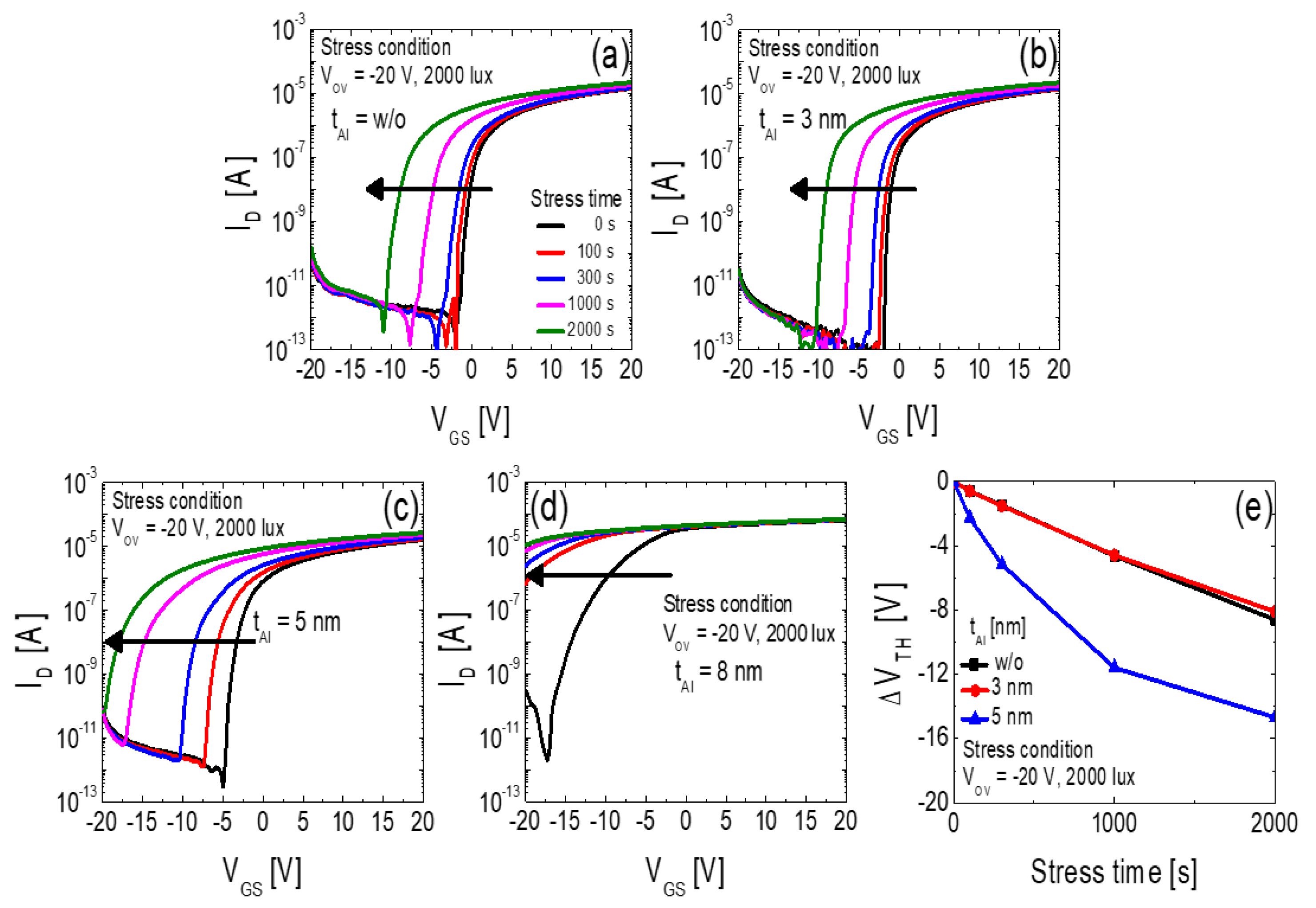
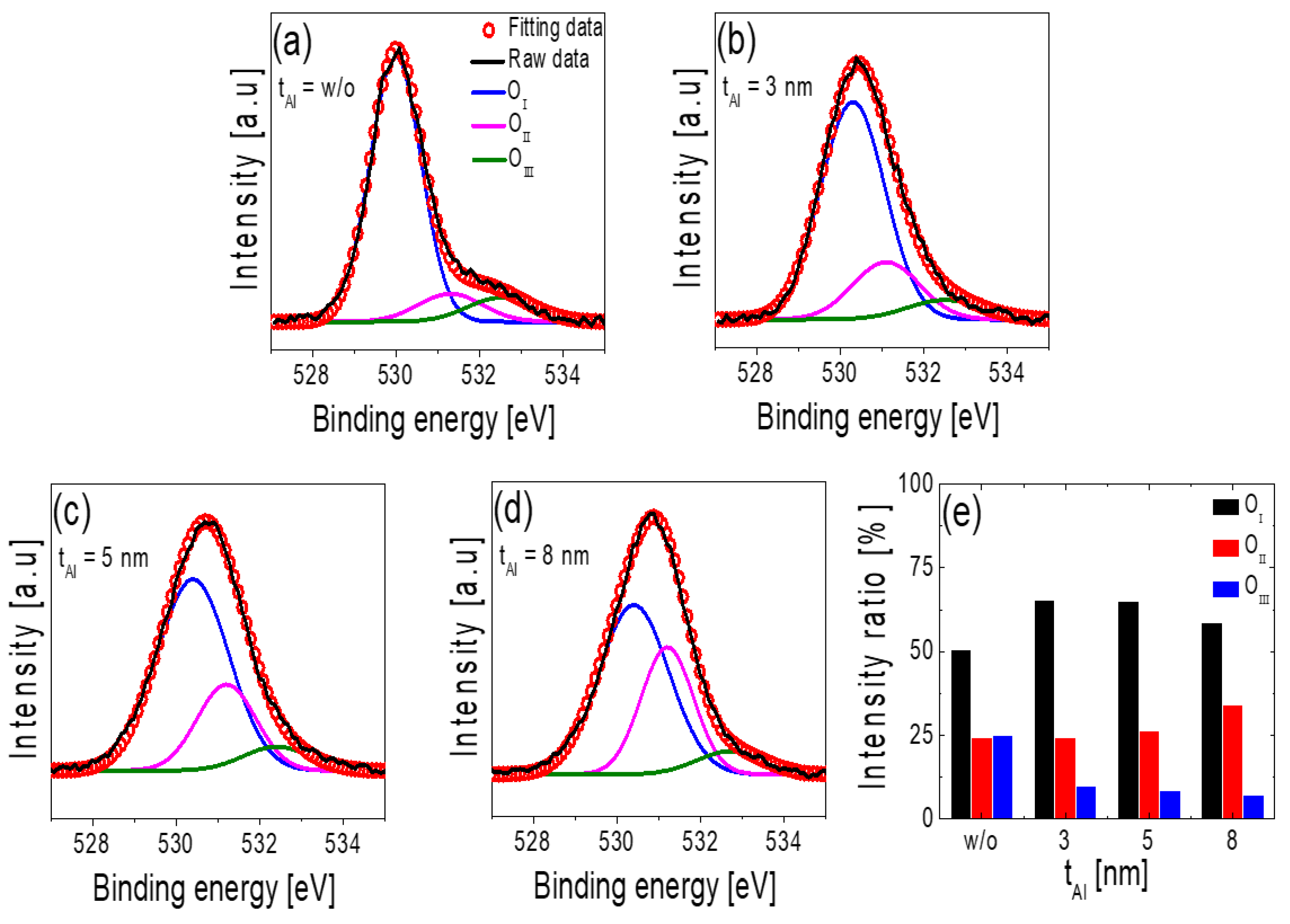
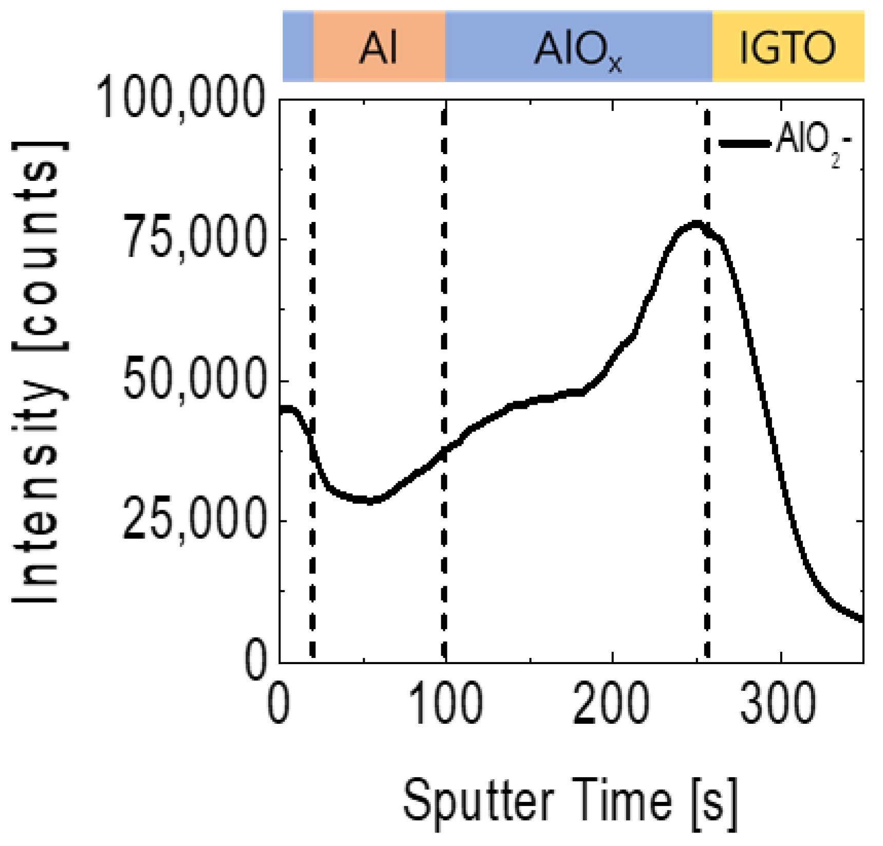
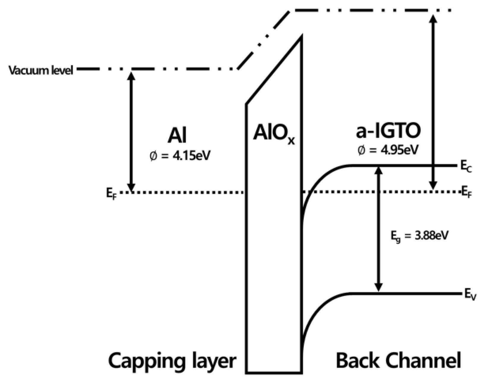
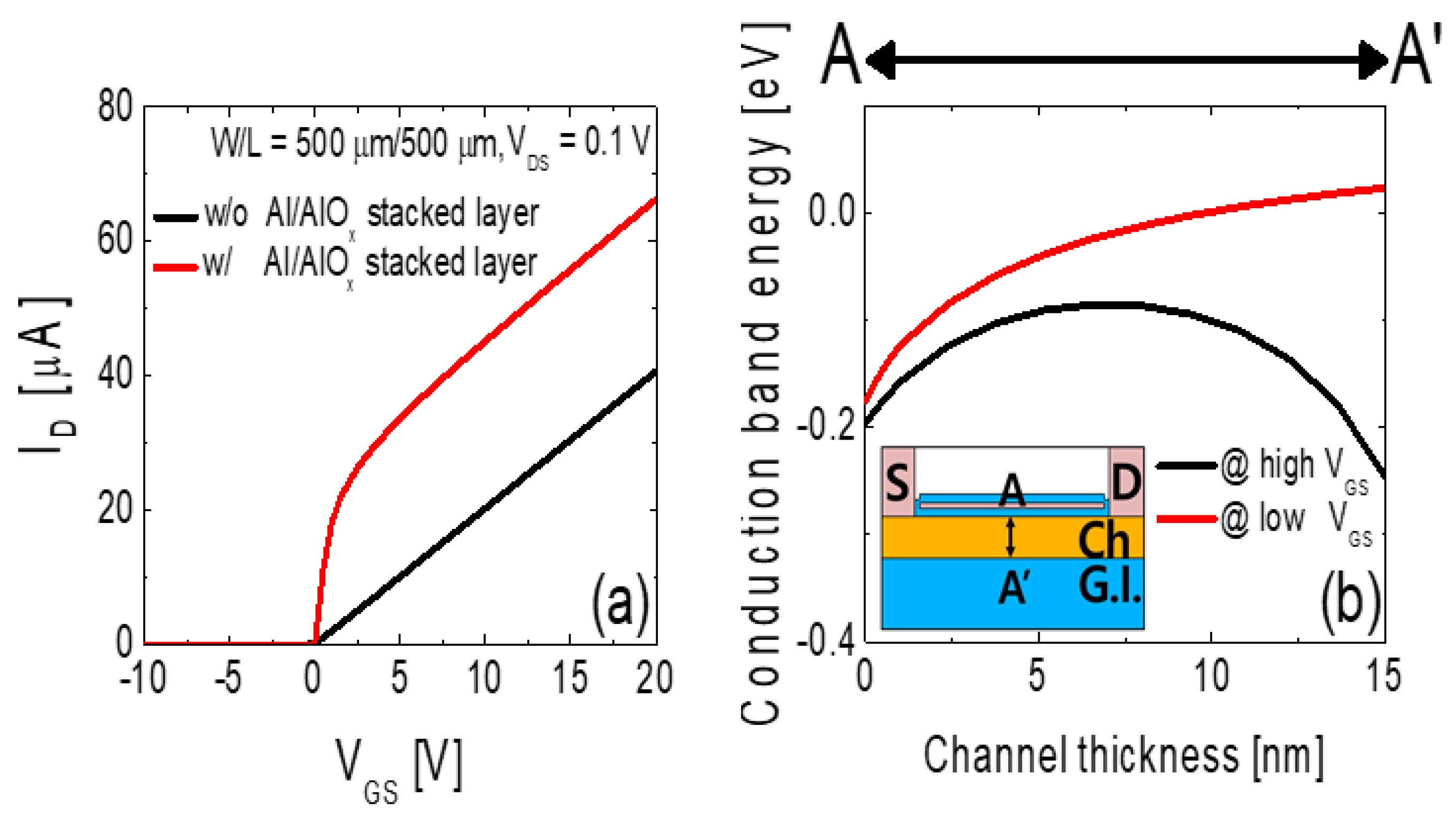
3. Results and Discussion

Figure 2a and b depict the representative transfer curves of the IGTO TFTs without and with 3, 5, and 8 nm thick Al capping layers on a semi-logarithmic (Figure 2a) and linear scale (Figure 2b). In Figure 2, ID, VGS, and VDS represent the drain current, gate-source voltage, and drain-source voltage, respectively. Electrical characterization was conducted by sweeping VGS from −20 to 20 V at VDS = 1.0 V for all IGTO TFTs. Table 1 lists the electrical parameters extracted from the IGTO TFTs without and with 3, 5, and 8 nm thick Al capping layers. The threshold voltage (VTH) was defined as the VGS value giving ID = W/L × 10−8 (A), and the field-effect mobility (µFE) was extracted from the maximum transconductance at VDS = 1.0 V using Equation (1):
μ F E = L g m W C i V D S
where Ci and gm are the gate dielectric capacitance per unit area and transconductance, respectively. The subthreshold swing (SS) was calculated from the semi-logarithmic scale transfer curve using Equation (2).
S S = d V G S d ( l o g I D )
The on/off current ratio (ION/OFF) was defined as the ratio between the maximum value of the on-current and the minimum value of the off-current for VGS ranging from −20 to 20 V at a VDS of 1.0 V. From Figure 2, it is observed that the IGTO TFTs without an Al capping layer and those having Al capping layers with tAls of 3 and 5 nm exhibit normal transfer characteristics; however, the TFT with tAl of 8 nm shows nonideal double slope characteristics in the transfer curve. μFE of the IGTO TFT increases and VTH shifts in the negative direction with an increase in tAl. The IGTO TFT with a 3 nm thick Al capping layer exhibits the minimum value of SS (0.2 V/dec) with satisfactory values of μFE (26.4 cm2/ V s) and VTH (−1.7 V). The obtained results clearly demonstrate that the thickness of the Al capping layer significantly influences the electrical performance of IGTO TFTs.
Figure 3a–d depict the time dependences of transfer curves for IGTO TFTs without and with 3, 5, and 8 nm thick Al capping layers, respectively, under a PBS of VOV = 20 V, where VOV = VGSVTH. Figure 3e summarizes the VTH shift (ΔVTH) obtained from IGTO TFTs without an Al capping layer and those with Al capping layers having different tAl values after each PBS time. The transfer curves shift in the positive direction for all IGTO TFTs as the PBS time increases. From Figure 3, it is observed that the formation of the Al capping layer effectively reduces the magnitude of ΔVTH after PBS in IGTO TFTs. However, no significant difference was observed in the PBS stabilities of the Al-capped IGTO TFTs having tAl values of 3, 5, and 8 nm. Figure 4a–d and e depict the time dependence of transfer curves and ΔVTH for IGTO TFTs without and with 3, 5, and 8 nm thick Al capping layers under an NBIS of VOV = −20 V and a white light (luminance: 2000 lx). Transfer curves shift in the negative direction for all IGTO TFTs as the NBIS time increases. Figure 4 shows that the magnitudes of ΔVTH after being exposed to NBIS have similar values for the uncapped IGTO TFT and that having a 3 nm thick Al capping layer. However, the transfer curves shift in the negative direction more significantly when tAl is greater than 3 nm. Figure 3 and Figure 4 show that the thickness of the Al capping layer strongly influences not only the electrical characteristics, but also the PBS and NBIS stabilities of the IGTO TFTs.
To elucidate the physical mechanism responsible for the observed phenomena, we compared the O1s spectra of the IGTO thin films without and with 3, 5, and 8 nm thick Al capping layers using XPS. Figure 5a–d depict the XPS O1s spectra of the IGTO thin films without and with 3, 5, and 8 nm thick Al capping layers, respectively. The XPS spectra were obtained for the middle sections of each IGTO thin film. The three sub-peaks at 530.0, 531.0, and 532.5 eV deconvoluted from the XPS spectra were assigned to the fully-coordinated metal ions (metal–oxygen lattice) (OI), oxygen deficiencies (OII), and weakly bonded oxygen components such as an interstitial oxygen and a hydroxyl group (OIII), respectively [19]. Figure 5e displays the relative areas of each sub-peak corresponding to OI, OII, and OIII, obtained from the IGTO thin films without and with Al capping layers. The XPS results in Figure 5 show that the weakly bonded oxygen-related components decreased from 25.0 to 10.0%, whereas the oxygen-deficient portion was maintained at 24.4% after the formation of the 3 nm thick Al capping layer. In contrast, a significant increase in the oxygen-deficient portion was observed after the formation of Al capping layers with tAl values greater than 3 nm (24.4% for uncapped IGTO thin film and that having a 3 nm thick Al capping layer, 26.5% for IGTO thin film with tAl value of 5 nm, and 34.1% for IGTO thin film with tAl value of 8 nm). These results imply that the thickness of the Al capping layer strongly affects the chemical composition of the underlying IGTO channel layer. The Gibbs free energies of formation (ΔGf) for In2O3, Ga2O3, SnO2, and Al2O3 are −830.7, −998.3, −516.0, and −1582.3 kJ/mol, respectively [25,26], and the lowest ΔGf value corresponding to that of Al2O3 implies that Al has a stronger oxidation power than In, Ga, and Sn. Therefore, the Al capping layer causes a reduction in the IGTO channel and becomes aluminum oxide (AlOX) after thermal annealing, which eliminates the weakly bonded oxygen such as an interstitial oxygen and a hydroxyl group and the lattice oxygen bonded to In, Ga, and Sn from the IGTO. The results in Figure 5 show that the gathering power of the oxygen species strongly depends on the thickness of the Al capping layer. The breaking of the cation–oxygen bonds requires a high activation energy; therefore, the 3 nm thick, thin Al layer eliminates only the weakly bonded oxygen such as an interstitial oxygen and a hydroxyl group. However, the Al capping layers thicker than 3 nm have a stronger gathering power of the oxygen species; therefore, the lattice oxygen is also eliminated from the IGTO after thermal annealing. The weakly bonded oxygen such as an interstitial oxygen and a hydroxyl group generates acceptor-like trap states near the conduction band (CB) edge and enhances electron trapping during the application of PBS in IGTO [27]. Therefore, a higher value of μFE, smaller value of SS, and better PBS stability of the IGTO TFT with a 3 nm thick Al capping layer can probably be attributed to the lower concentration of the weakly bonded oxygen species within the IGTO channel layer than the IGTO TFT without a capping layer. Oxygen vacancies (VO) generate shallow and deep donor states within the IGTO channel layer [28,29]. Shallow donor states provide electrons to the CB; therefore, the electron concentration increases as the number of VO increases within the IGTO channel layer. The increase in the electron concentration enhances the formation of the percolation conduction path in IGTO and makes it difficult to turn off the TFT [30,31,32]. In addition, a higher carrier concentration within the channel increases the SS value of the TFT [33,34]. Therefore, a lower value of VTH and higher values of μFE and SS in the 5 and 8 nm thick Al-capped IGTO TFTs than in the uncapped and 3 nm thick Al-capped IGTO TFTs can be attributed to the larger concentration of VO within the IGTO channel layer caused by the stronger oxidation power of the thicker Al capping layer. The poorest NBIS stability exhibited by TFTs with tAl values of 5 and 8 nm can also be attributed to the high density of VO within the IGTO channel, because the doubly ionized VOs are generated from VO and diffuse toward the gate dielectric/channel interface under NBIS [35,36].
The non-ideal double slope transfer characteristics of the Al-capped IGTO TFT with tAl of 8 nm are considered to be a result of the partial oxidation of the Al capping layer during thermal annealing. Figure 6 displays the time-of-flight secondary ion mass spectrometry (ToF-SIMS) negative ion depth profile for AlO2- ions obtained from the 8 nm thick Al capping layer in the fabricated Al-capped IGTO TFT. Figure 6 shows that the AlO2-signal exhibits high values at the surface and near the IGTO channel layer; however, relatively lower values of the AlO2-signal are observed between these two regions. Considering that the AlO2-ion is a representative of AlOX, this implies that the 8 nm thick capping layer is composed of three regions: AlOX (near the surface), Al, and AlOX (near IGTO), as depicted in Figure 6. The AlOX layers at the surface and near the IGTO layer are likely to be formed as a result of the oxidation of the Al capping layer by oxygen in the environmental air and that in the IGTO channel layer, respectively. Figure 7 illustrates the schematic energy band diagram for the Al-AlOX-Si MOS capacitor, where the Φ and Eg values of the IGTO were determined to be 4.95 and 3.88 eV, respectively. Considering that the Φ value of Al (4.0 ~ 4.28 eV) [37,38] is smaller than that of the IGTO, the accumulation layer can be formed at the interface between the AlOX and IGTO, as observed in Figure 7, which can act as the parasitic channel causing the non-ideal double slope transfer characteristics of the Al-capped IGTO TFT with tAl of 8 nm.
Figure 8a displays the technology computer-aided design (TCAD) simulation results for the transfer characteristics of the IGTO TFT with and without an Al/AlOX stacked layer on top of the IGTO channel layer. The simulation results show that the transfer characteristics of the IGTO TFT with an Al/AlOX stacked layer exhibit non-ideal double slope transfer characteristics. Figure 8b depicts the TCAD simulation results for the conduction band energy in the IGTO TFT with an Al/AlOX stacked layer along A-A’ in the inset figure. The TCAD simulation results in Figure 8b show that the main channel is formed near the top AlOX layer at low VGS’s, but is formed near the bottom SiO2 layer at high VGS’s. These results show that the parasitic channel formed between the AlOX and IGTO is the reason for the non-ideal double slope transfer characteristics of the Al-capped IGTO TFT with tAl of 8 nm.

4. Conclusions

In this work, we studied the effect of Al capping layer thickness on the electrical performance and stability of high-mobility IGTO TFTs. An Al capping layer with tAl values of 3, 5, and 8 nm were deposited on top of the IGTO thin film and the fabricated IGTO TFTs without and with Al capping layers were thermally annealed at 200 °C for 1 h in air. Among the IGTO TFTs, the TFT with a 3 nm thick Al capping layer exhibited excellent electrical properties and better electrical stability under PBS and NBIS than the other TFTs. The IGTO TFT without an Al capping layer exhibited a lower value of μFE, higher value of SS, and inferior PBS stability compared with the IGTO TFT with a 3 nm thick Al capping layer. The IGTO TFTs with 5 and 8 nm thick Al capping layers exhibited significantly lower values of VTH, higher values of SS, and poorer NBIS stabilities compared with the IGTO TFT with a 3 nm thick Al capping layer. The observed phenomenon was attributed to the thickness dependent oxidation power of the Al capping layer. The oxidation power of the Al capping layer increased with increasing tAl and 3 nm was found to be the optimum thickness of the Al capping layer, which can selectively eliminate the weakly bonded oxygen species from the IGTO channel layer without significantly generating VO within the IGTO. Our experimental results show that the electrical performance and stability of IGTO TFTs can be effectively improved by forming an Al capping layer with optimal thickness.

Author Contributions

Conceptualization, H.-S.C. and H.-I.K.; experiment, H.-S.C., H.-S.J., S.-H.H. and D.-H.L.; data analysis, H.-S.C. and H.-I.K., writing—original draft preparation, H.-S.C.; supervision, H.-I.K.; writing—review and editing, H.-I.K. All authors have read and agreed to the published version of the manuscript.

Funding

This research was supported by Samsung Display Co., Ltd. and the Chung-Ang University Research Scholarship Grants in 2020. In particular, the authors thank Shinhyuk Kang (Samsung Corning Advanced Glass) for supporting the IGTO sputter target for this work.

Conflicts of Interest

The authors declare no conflict of interest.

References

  1. Fortunato, E.; Barquinha, P.; Martins, R. Oxide semiconductor thin-film transistors: A review of recent advances. Adv. Mater. 2012, 24, 2945–2986. [Google Scholar] [CrossRef] [PubMed]
  2. Kamiya, T.; Hosono, H. Material characteristics and applications of transparent amorphous Oxide semiconductors. NPG Asia Mater. 2010, 2, 15–22. [Google Scholar] [CrossRef] [Green Version]
  3. Jang, J.T.; Ahn, G.H.; Choi, S.-J.; Kim, D.M.; Kim, D.H. Control of the boundary between the gradual and abrupt modulation of resistance in the schottky barrier tunneling-modulated amorphous Indium-Gallium-Zinc-Oxide memristors for neuromorphic computing. Electronics 2019, 8, 1087. [Google Scholar] [CrossRef] [Green Version]
  4. Park, J.-S.; Maeng, W.-J.; Kim, H.-S.; Park, J.-S. Review of recent developments in amorphous Oxide semiconductor thin-film transistor devices. Thin Solid Films 2012, 520, 1679–1693. [Google Scholar] [CrossRef]
  5. Kamiya, T.; Nomura, K.; Hosono, H. Present status of amorphous In–Ga–Zn–O thin-film transistors. Sci. Technol. Adv. Mater. 2010, 11, 044305. [Google Scholar] [CrossRef] [PubMed]
  6. Kikuchi, Y.; Nomura, K.; Yanagi, H.; Kamiya, T.; Hirano, M.; Hosono, H. Device characteristics improvement of a-In–Ga–Zn–O TFTs by low-temperature annealing. Thin Solid Films 2010, 518, 3017–3021. [Google Scholar] [CrossRef]
  7. Kim, S.-C.; Jeon, Y.-W.; Kim, Y.-S.; Kong, D.-S.; Jung, H.-K.; Bae, M.-K.; Lee, J.-H.; Ahn, B.-D.; Park, S.-Y.; Park, J.-H.; et al. Impact of oxygen flow rate on the instability under positive bias stresses in DC-sputtered amorphous InGaZnO thin-film transistors. IEEE Electron Device Lett. 2012, 33, 62–64. [Google Scholar] [CrossRef]
  8. Yabuta, H.; Sano, M.; Abe, K.; Aiba, T.; Den, T.; Kumomi, H.; Nomura, K.; Kamiya, T.; Hosono, H. High mobility thin-film transistor with amorphous InGaZnO4 channel fabricated by room temperature rf magnetron sputtering. Appl. Phys. Lett. 2006, 89, 112123. [Google Scholar] [CrossRef]
  9. Fuh, C.-S.; Liu, P.-T.; Huang, W.-H.; Sze, S.M. Effect of annealing on defect elimination for high mobility amorphous Indium-Zinc-Tin-Oxide thin-film transistor. IEEE Electron Device Lett. 2014, 35, 1103. [Google Scholar] [CrossRef]
  10. Paine, D.-C.; Yaglioglu, B.; Beiley, Z.; Lee, S.-H. Amorphous IZO-based transparent thin film transistor. Thin Solid Films 2008, 516, 5894–5898. [Google Scholar] [CrossRef]
  11. Ruan, D.-B.; Liu, P.-T.; Chiu, Y.-C.; Kan, K.-Z.; Yu, M.-C.; Chien, T.-C.; Chen, Y.-H.; Kuo, P.-Y.; Sze, S.-M. Investigation of low operation voltage InZnSnO thin-film transistors with different high-k gate dielectric by physical vapor deposition. Thin Solid Films 2018, 660, 885–890. [Google Scholar] [CrossRef]
  12. Jeong, H.-S.; Cha, H.S.; Hwang, S.H.; Kwon, H.-I. Effects of annealing atmosphere on electrical performance and stability of high-mobility Indium-Gallium-Tin Oxide thin-film transistors. Electronics 2020, 9, 1875. [Google Scholar] [CrossRef]
  13. Hur, J.-S.; Kim, J.-O.; Kim, H.-A.; Jeong, J.-K. Stretchable polymer gate dielectric by ultraviolet-assisted Hafnium Oxide doping at low temperature for high-performance Indium Gallium Tin Oxide transistors. ACS Appl. Mater. Interfaces 2019, 11, 21675–21685. [Google Scholar] [CrossRef] [PubMed]
  14. Kim, J.-O.; Hur, J.-S.; Kim, D.-S.; Lee, B.-M.; Jung, J.-M.; Kim, H.-A.; Chung, U.-J.; Nam, S.-H.; Hong, Y.T.; Park, K.-S.; et al. Network structure modification-enabled hybrid polymer dielectric film with Zirconia for the stretchable transistor applications. Adv. Funct. Mater. 2020, 30, 1906647. [Google Scholar] [CrossRef]
  15. Park, J.-S.; Kim, T.-W.; Stryakhilev, D.; Lee, J.-S.; An, S.-G.; Pyo, Y.-S.; Lee, D.-B.; Mo, Y.-G.; Jin, D.-U.; Chung, H.-K. Flexible full color organic light-emitting diode display on polyimide plastic substrate driven by amorphous indium gallium zinc oxide thin-film transistors. Appl. Phys. Lett. 2009, 95, 013503. [Google Scholar] [CrossRef]
  16. Carey, P.-G.; Smith, P.-M.; Theiss, S.-D.; Wickboldt, P. Polysilicon thin film transistors fabricated on low temperature plastic substrates. J. Vac. Sci. Technol. 1999, 17, 1946–1949. [Google Scholar] [CrossRef]
  17. Jeong, H.-J.; Ok, K.-C.; Park, J.; Lim, J.-H.; Cho, J.-H.; Park, J.-S. Stability improvement of In–Sn–Ga–O thin-film transistors at low annealing temperatures. IEEE Electron Device Lett. 2015, 36, 1160–1162. [Google Scholar] [CrossRef]
  18. Kim, H.-A.; Kim, J.O.; Hur, J.S.; Son, K.-S.; Lim, J.H.; Cho, J.; Jeong, J.K. Achieving high mobility in IGTO thin-film transistors at a low temperature via film densification. IEEE Trans. Electron Devices 2018, 65, 4854–4860. [Google Scholar] [CrossRef]
  19. Oh, C.; Jang, H.; Kim, H.W.; Jung, H.; Park, H.; Cho, J.; Kim, B.S. Influence of oxygen partial pressure in In–Sn–Ga–O thin-film transistors at a low temperature. J. Alloy. Compd. 2019, 805, 211–217. [Google Scholar] [CrossRef]
  20. Lee, B.-H.; Sohn, A.; Kim, S.-S.; Lee, S.-Y. Mechanism of carrier controllability with metal capping layer on amorphous Oxide SiZnSnO semiconductor. Sci. Rep. 2019, 9, 1–7. [Google Scholar] [CrossRef] [Green Version]
  21. Choi, J.-Y.; Lee, B.-H.; Kim, S.-S.; Lee, S.-Y. Metal capping on Silicon Indium Zinc Oxide semiconductor for high performance thin film transistors processed at 150°C. J. Nanosci. Nanotechnol. 2017, 17, 3397–3400. [Google Scholar] [CrossRef]
  22. Shin, Y.-W.; Kim, S.-T.; Kim, K.-T.; Kim, M.-Y.; Oh, S.; Jeong, J.-K. The mobility enhancement of Indium Gallium Zinc Oxide transistors via low-temperature crystallization using a Tantalum catalytic layer. Sci. Rep. 2017, 7, 10885. [Google Scholar] [CrossRef] [PubMed]
  23. Ji, H.; Hwang, A.-Y.; Lee, C.-K.; Yun, P.-S.; Bae, J.-U.; Park, K.-S.; Jeong, J.-K. Improvement in field-effect mobility of Indium Zinc Oxide transistor by Titanium metal reaction method. IEEE Trans. Electron Devices 2015, 62, 1195–1199. [Google Scholar] [CrossRef]
  24. Kim, T.-H.; Kim, M.-J.; Lee, J.-W.; Jeong, J.-K. Boosting carrier mobility in Zinc Oxynitride thin-film transistors via Tantalum oxide encapsulation. ACS Appl. Mater. Interfaces 2019, 11, 22501–22509. [Google Scholar] [CrossRef]
  25. Park, J.-M.; Kim, H.-D.; Jang, S.-C.; Kim, M.-J.; Chung, K.-B.; Kim, Y.-J.; Kim, H.-S. Improved field-effect mobility of In–Ga–Zn–O TFTs by oxidized metal layer. IEEE Trans. Electron Devices 2020, 67. [Google Scholar] [CrossRef]
  26. Kojima, T.; Kameoka, S.; Tsai, A.P. Heusler Alloys: A group of novel catalysts. ACS Omega 2017, 2, 147–153. [Google Scholar] [CrossRef]
  27. Robertson, J.; Guo, Y. Light induced instability mechanism in amorphous InGaZn oxide semiconductors. Appl. Phys. Lett. 2014, 104, 162102. [Google Scholar] [CrossRef]
  28. Kamiya, T.; Nomura, K.; Hirano, M.; Hosono, H. Electronic structure of oxygen deficient amorphous oxide semiconductor a-InGaZnO4–x: Optical analyses and first-principle calculations. Phys. Stat. Sol. 2008, 5, 3098–3100. [Google Scholar] [CrossRef]
  29. Lee, J.-S.; Kim, D.-J.; Lee, S.-H.; Cho, J.-H.; Park, H.-G.; Jang, J. High field effect mobility, amorphous In-Ga-Sn-O thin-film transistor with no effect of negative bias illumination stress. IEEE Electron Device Lett. 2019, 40, 1443–1446. [Google Scholar] [CrossRef]
  30. Lee, S.; Ghaffarzadeh, K.; Nathan, A.; Robertson, J.; Jeon, S.; Kim, C.; Song, I.-H.; Chung, U.I. Trap-limited and percolation conduction mechanisms in amorphous oxide semiconductor thin film transistors. Appl. Phys. Lett. 2011, 98, 203508. [Google Scholar] [CrossRef]
  31. Shao, L.; Nomura, K.; Kamiya, T.; Hosono, H. Operation characteristics of thin-film transistors using very thin amorphous In–Ga–Zn–O channels. Electrochem. Solid-State Lett. 2011, 14, H197. [Google Scholar] [CrossRef]
  32. Barquinha, P.; Pimentel, A.; Marques, A.; Pereira, L.; Martins, R.; Fortunato, E. Influence of the semiconductor thickness on the electrical properties of transparent TFTs based on indium zinc oxide. J. Non-Cryst. Solids 2006, 352, 1749. [Google Scholar] [CrossRef]
  33. Wang, D.; Zhao, W.; Li, H.; Furuta, M. Drain current stress-induced instability in amorphous InGaZnO thin-film transistors with different active layer thicknesses. Materials 2018, 11, 559. [Google Scholar] [CrossRef] [PubMed] [Green Version]
  34. Woo, C.H.; Kim, Y.Y.; Kong, B.H.; Cho, H.K. Effects of the thickness of the channel layer on the device performance of InGaZnO thin-film-transistors. Surf. Coat. Technol. 2010, 205, S168–S171. [Google Scholar] [CrossRef]
  35. Mativenga, M.; Um, J.-G.; Jang, J. Reduction of bias and light instability of mixed oxide thin-film transistors. Appl. Sci. 2017, 7, 885. [Google Scholar] [CrossRef] [Green Version]
  36. Um, J.-G.; Mativenga, M.; Jang, J. Mechanism of positive bias stress-assisted recovery in amorphous-indium-gallium-zincoxide thin-film transistors from negative bias under illumination stress. Appl. Phys. Lett. 2013, 103, 033501. [Google Scholar] [CrossRef]
  37. Kumar, B.; Kaushik, B.K.; Negi, Y.S. Perspectives and challenges for organic thin film transistors: Materials, devices, processes and applications. J. Mater. Sci. Mater. Electron. 2014, 25, 1–30. [Google Scholar] [CrossRef]
  38. Lang, N.D.; Kohn, W. Theory of metal surfaces: Work function. Phys. Rev. B 1971, 3, 1215. [Google Scholar] [CrossRef]
Figure 1. (a) Schematic view and (b) optical image of the fabricated Al-capped indium–gallium–tin oxide (IGTO) thin-film transistors (TFTs). ITO, indium–tin oxide.
Electronics 09 02196 g001
Figure 2. Representative transfer curves of the IGTO TFTs without and with 3, 5, and 8 nm thick Al capping layers on a (a) semi-logarithmic and (b) linear scale. Electrical characterization was conducted by sweeping VGS from −20 to 20 V at VDS = 1.0 V.
Electronics 09 02196 g002
Figure 3. Time dependence of the transfer curves for IGTO TFTs (a) without and with (b) 3, (c) 5, and (d) 8 nm thick Al capping layers, under a positive bias stress (PBS) of VOV = 20 V. (e) ΔVTH obtained from IGTO TFTs without and with 3, 5, and 8 nm thick Al capping layers after each PBS time.
Electronics 09 02196 g003
Figure 4. Time dependence of the transfer curves for IGTO TFTs (a) without and with (b) 3, (c) 5, and (d) 8 nm thick Al capping layers, under a negative bias illumination stress (NBIS) of VOV = −20 V and a white light (luminance: 2000 lx). (e) ΔVTH obtained from IGTO TFTs without and with 3 and 5 nm thick Al capping layers after each NBIS time.
Electronics 09 02196 g004
Figure 5. X-ray photoelectron spectroscopy (XPS) O1s spectra of the IGTO thin films (a) without and with (b) 3, (c) 5, and (d) 8 nm thick Al capping layers, obtained at the middle of the thin films. (e) Relative areas of each peak corresponding to OI (metal–oxygen lattice), OII (oxygen deficiencies), and OIII (weakly bonded oxygens), obtained from the IGTO thin films without and with 3, 5, and 8 nm thick Al capping layers.
Electronics 09 02196 g005
Figure 6. Time-of-flight secondary ion mass spectrometry (ToF-SIMS) negative ion depth profile for AlO2-ions obtained from the 8 nm thick Al capping layer in the fabricated Al-capped IGTO TFT.
Electronics 09 02196 g006
Figure 7. Schematic energy band diagram for the Al-AlOX-Si MOS capacitor.
Electronics 09 02196 g007
Figure 8. (a) Technology computer-aided design (TCAD) simulation results for the transfer characteristics of the IGTO TFT without and with an Al/AlOX stacked layer on top of the IGTO channel layer. (b) TCAD simulation results for the conduction band energy in the IGTO TFT with an Al/AlOX stacked layer along A-A’ in the inset figure.
Electronics 09 02196 g008
Table 1. Electrical parameters extracted from the indium–gallium–tin oxide (IGTO) thin-film transistors (TFTs) without and with 3, 5, and 8 nm thick Al capping layers.
tAl [nm]VTH [V]μFE [cm2·V−1·S−1]SS [V/decade]ION/OFF
0 (w/o Al)−0.125.90.423.51 × 10 7
3−1.726.40.205.52 × 10 8
5−3.727.60.373.90 × 10 7
8−14.0-1.312.50 × 10 6
Publisher’s Note: MDPI stays neutral with regard to jurisdictional claims in published maps and institutional affiliations.

