1. Introduction
In high power applications such as medium voltage motor drives, solar cells, vehicles, and most recently, wind generation system, etc., multilevel topologies introduced in [
1] have been widely applied to reduce harmonic in the grid current, to downsize the physical filter size, and to mitigate the switching losses of the used devices as compared with the conventional two-level pulse width modulation (PWM) inverter. These multilevel topologies allow the output voltage to be closer to the sinusoidal wave by increasing the number of voltage levels, and reducing the harmonic distortion, as reported in the literature [
2,
3,
4]. The major multilevel topologies that have been studied are neutral point clamped (NPC) [
5,
6], active net point clamped (ANPC) [
7,
8,
9], flying capacitor (FC) [
10,
11,
12], and cascaded multilevel inverter (CMLI) [
13,
14]. The ANPC application has a high cost since it has a relatively large number of switching devices. The capacitor used in FC requires precharging, and the high number of flying capacitors required with increasing output levels reduces system reliability. The disadvantages of CMLI are the complexity of synchronization and the unbalanced power losses between power modules. Among these topologies, the three-level neutral point clamped (NPC) voltage source inverter (VSI) is the most popular topology as compared with other three-level topologies because it has some advantages such as simple operating sequence, low voltage stress, and low switching losses [
15,
16].
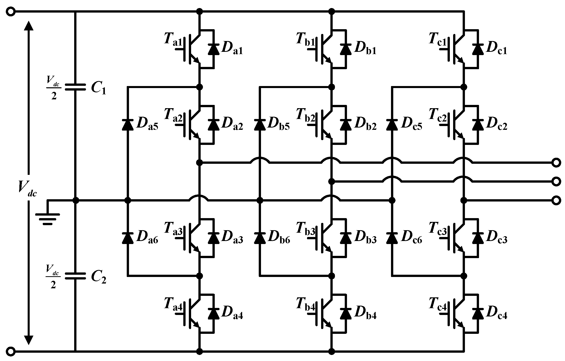
Figure 1 illustrates a three-level NPC VSI topology.
Each leg consists of four switching devices which are connected in series, two diodes, and a neutral point of dc-link as shown in
Figure 1.
The performance including the efficiency and total harmonic distortion (THD) of the three-level NPC VSI is affected by the PWM method such as sinusoidal pulse width modulation (SPWM), space vector pulse width modulation (SVPWM), and discontinuous pulse width modulation (DPWM), etc.; the available output voltage area is determined depending on the PWM method [
17,
18,
19,
20]. The previously explained PWM techniques all require dead time when transitioning from positive to zero, or reverse, switching transition conditions. In this transition time, the switching device,
Tx1, is turned off and the switching device,
Tx3, is turned on, in parallel. During the transition time, the dead time is applied to prevent a short circuit caused by the on/off delay of the switching devices.
However, the dead time in the complementary switching method causes distortion in the output voltage, and therefore increases the THD in the phase current. For this reason, dead-time compensation methods are widely studied to reduce the THD in phase current [
21,
22,
23,
24]. In [
21], the authors proposed a method to improve the harmonic components caused by dead time by applying the offset voltage which consisted of the reference voltage and distorted output voltage in an inverter. Selective harmonic elimination (SHE) modulation is also one of the ways to solve harmonic component, considering dead-time effect [
25]. However, since this method is based on the PWM which operates complementarily, these methods have the characteristic of turning on the switching device even when there is no current flowing into the switching devices.
Another research integrated the sixth harmonic of the synchronous d-axis proportional-integral (PI) current regulator [
22]. This method imposes high computational burden and is difficult to realize, because of the detection of harmonics by integrated operation with integral controller. A previous study used a parameter adjustment mechanism for adaptive dead-time compensation [
23]. Because this method utilized the dc-bus voltage and three-phase voltage, it was difficult to achieve an accurate effect if an imbalance of three-phase voltage and dc-bus voltage existed. In [
26], dead-time compensation was performed with a dead-time correction state machine. This method was based on the error from measured three-phase voltage and current, and sensitiveness existed from the disturbance, which was a disadvantage.
In the case of the previous studies, there are limitations to the compensation of current disturbance due to dead time, because of the modulation or complicated control configuration and mechanism, and based on various infarction signals.
In this paper, to solve these limitations, the zero dead-time width modulation (ZDPWM) method is proposed which does not need the dead-time, and therefore there improve the distortion of output current. A short circuit which is caused by the on/off delay of switching devices does not appear when the complementary switching operation is not used. Thus, in this paper, we describe the ZDPWM method that operates without dead time, and how this PWM is implemented by comparing the carrier and reference voltage. We also suggest an improved method that can solve the sampling delay of a microcontroller unit (MCU) that is seen in the experiment.
This paper is organized as follows: In
Section 2, we describe the basic structure and theory of the existing three-level NPC topology; in
Section 3, we describe the analysis of the proposed ZDPWM method and how to implement the proposed technique; in
Section 4, we describe the impact of sampling delay on the proposed ZDPWM method and the technique to improve this; in
Section 5, we describe the simulation and experimental results for validation of the proposed control; and in
Section 6, we provide the conclusions.
2. Configuration of the Three-level Neutral Point Clamped (NPC) Inverter and Operation Principle
In this section, first, we describe the basic configuration and operating principles of NPC topology and the effects of dead time before describing the proposed techniques.
The three-level NPC inverter, as shown in
Figure 1, is connected to the neutral point, the neutral point clamp diode, and the dc-link capacitor, each leg consists of four switches, and two neutral point clamp diodes. Since the two neutral point clamp diodes are connected to the neutral point of the dc-link, unlike the two-level inverter, an output state of "zero" is possible.
Table 1 shows the switching state of the three-level NPC inverter according to the output voltage. Switching states can be divided into three states depending on the output voltage.
Figure 2 shows the flow of current with switching status in a three-level NPC inverter. The state, in
Figure 2a, outputs a voltage of "positive" with current flowing under load from the top capacitor and switches
Tx1 and
Tx2 on one leg.
Tx1 and
Tx3,
Tx2 and
Tx4 perform reciprocal actions, therefore,
Tx3 and
Tx4 are off. The state, in
Figure 2b, is that the current is flowing from the neutral point to the load, the voltage output is "zero", with switches
Tx2 and
Tx3 on and switches
Tx1 and
Tx4 off. The state, in
Figure 2c, is that the current is flowing from the lower capacitor to the load, the voltage output is "negative", with switches
Tx3 and
Tx4 on and switches
Tx1 and
Tx2 off.
These three-level NPC inverters can be designed to have a lower voltage on each switch than conventional two-level inverters because one leg consists of four switches. In addition, the level of voltage is higher than that of a two-level inverter, therefore, the THD is lower. All elements are switched to the fundamental frequency, which gives the inverter a high efficiency advantage [
27].
The three-level NPC is generally adapting SVPWM, the same as the two-level inverters [
28]. With SVPWM, the three-level NPC inverter consists of a total of 27 switching states and 19 voltage vectors, as shown in
Figure 3.
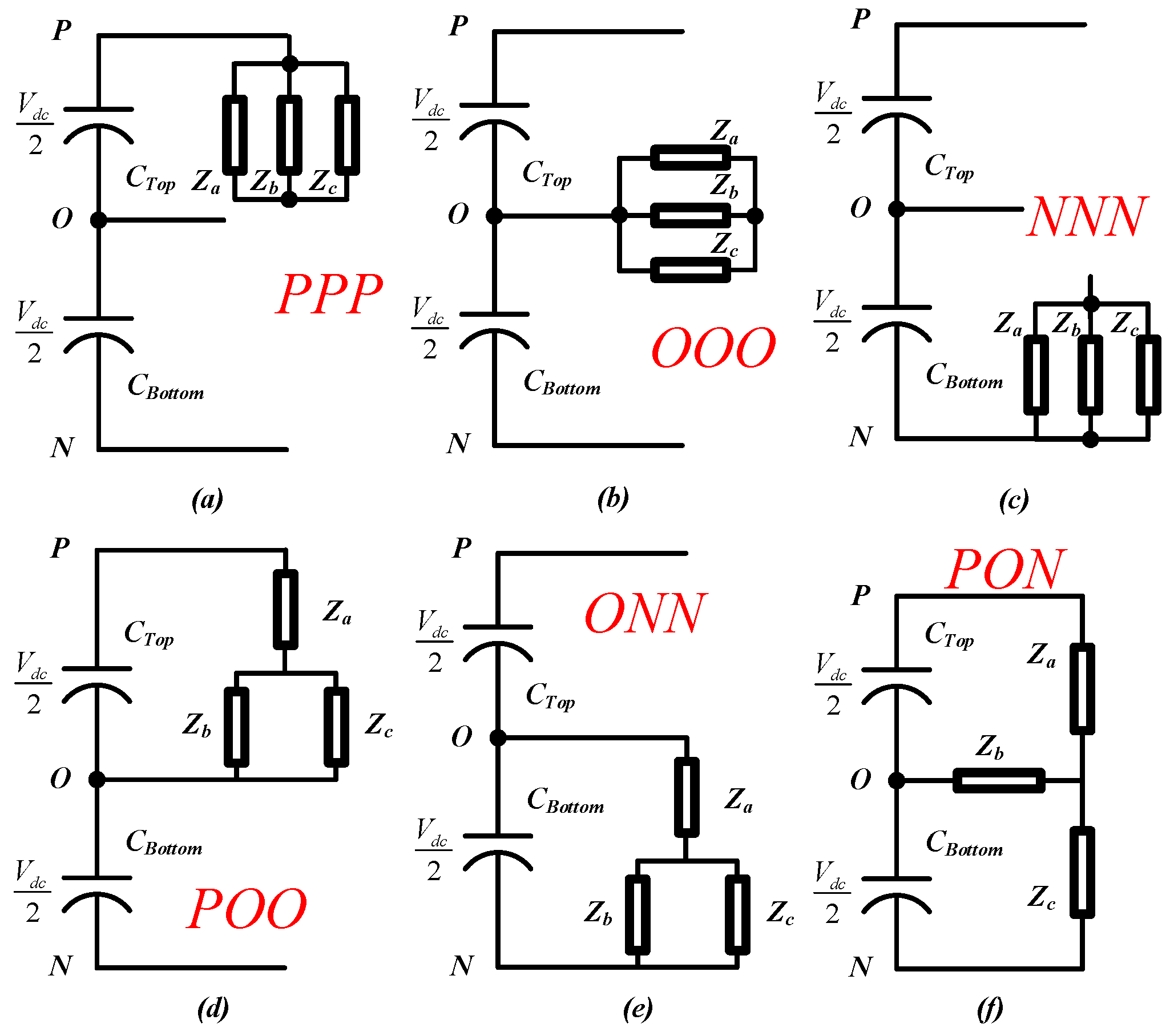
At this time, vectors requiring dead time are divided into three forms, as shown in
Figure 4, depending on the state of the load. First, a unit vector, representing 120 degrees phase displacement, is as shown in Equation (1), in order to express the phase voltage of the load as:
The space vector of the phase voltage of the load can be expressed as shown in Equation (2):
With equation (2), the voltage vector of the zero vector in
Figure 4a–c can be expressed as (3):
Figure 4d,e shows a small vector. When switching states are (POO) and (ONN), voltage vectors can be expressed in the following ways:
In addition,
Figure 4f shows the medium vector, and if the switching state is (PON), the dc-link neutral point is connected to the load stage, which affects the voltage variation of the neutral point. In the above state, the voltage vector may be shown as follows:
In order to make the above load conditions, the three-level NPC inverter must perform a complementary operation of four insulated gate bipolar transistor (IGBT) and two reverse parallel diodes, as described earlier.
Figure 5 shows the characteristics of power switching devices that use dead time, when performing complementary operation. The upper side represents switching signals, and the bottom side represents collector-emitter voltage and output current. As shown in
Figure 5, the transition between the on/off states may cause a short circuit, due to the time difference between rising time and falling time, and therefore dead time is applied to the on/off signals to prevent such short circuit accidents. However, due to the effect of dead time, an error occurs between the commanded voltage and the actual voltage. These voltage errors vary with the inverter current direction.
Figure 6 shows the switching state and output voltage during dead time. Switch
Tx2 is always on, and
Tx4 is always off. When the direction of the current is
io > 0, applying the dead time by
tdead to switch
Tx1 causes an error between the command switching and the actual switching, resulting in an error voltage equal to
Verror in the output voltage. Similarly, when the direction of the current is
io < 0, applying dead time to
Tx3 produces a voltage error as much as
Verror at the output voltage. The error voltage generated by such dead time causes distortion of the output current, higher distortion of the electric wave, and lower stability of the system, due to the distorted output current [
29].
3. Proposed Zero Dead-Time PWM Method
In this section, we describe the proposed zero dead-time PWM (ZDPWM) which totally removes dead-time utilization for PWM generation, in order to improve the previously explained current distortion caused by dead time in a three-level NPC inverter.
Figure 7 shows the switching mode according to the reference voltage and phase current. The proposed method focuses on turning on the switching devices which are flowing the current, and is divided into four operation areas depending on the direction of the reference voltage and phase current as shown in
Figure 7b–e. The reference voltage and phase current conditions in each section are as follows:
First,
Figure 7b illustrates when the direction of the current is in the “+” direction. In section I, the switch
Tx3, which is affected by dead time, does not turn on when switching from “positive” to “zero” state. Therefore, because it does not operate the more than three switching devices, there is no dead-time interval without implementing the complementary operation.
Figure 7c illustrates when the direction of the current is in the “+” direction, as in case of
Figure 7b. In Section II, switch
Tx3, which is affected by dead time, does not turn on when switching from the “negative” to “zero” state. Therefore, the complementary operation is also not performed in Section II.
Figure 7d shows when the direction of the current is in the “−” direction. In Section III, the switch
Tx2, which is affected by dead time does not turn on when switching from the “negative” to “zero” state. Thus, because it does not operate the more than three switching devices, there is also no implementation of the complementary operation.
Figure 7e illustrates when the direction of the current is in the “+” direction, as in case of the
Figure 7d. In Section IV, the switch
Tx2 does not turn on when switching from the “positive” to “zero” state. Therefore, the complementary operation is also not implemented in Section IV. As a result, the switching states can remove dead time from any of the operation modes as there is no short circuit fault resulted from turn on/off delay between the switching transient [
30].
Figure 8 shows the switching signal and reference voltage waveforms of phase A of the proposed ZDPWM method used in the three-level NPC VSI. Depending on the direction of the output current, two offset voltages
Va_offsetx are generated, and the magnitude of the offset voltage is determined by the maximum modulation index (MI), as shown in
Figure 8 and Equation (7) as:
The proposed technique is based on the SVPWM method; the maximum MI value of SVPWM is 1.1547. When the SVPWM generates a voltage reference from the output of the PI current controller, the offset value is designated as the maximum MI value, as described in Equation (7), in order to use the same maximum capable output voltage as the maximum voltage of SVPWM.
Two new reference voltages are generated by adding two offset voltage to the reference voltage, as shown in
Figure 8. On the one hand, when
V*a_ref1, which is generated by merging with the “−” offset voltage, is greater than the upper carrier
Carriertop, the switching signal is generated by switch
Tx1, and when
V* a_ref1 is greater than the lower carrier
Carrierbottom, the switching signal is generated by switch
Tx2.
On the other hand, when
V*a_ref2, which is generated by merging with the “+” offset voltage, is less than the upper carrier
Carriertop, the switching signal is generated by switch
Tx3, and when
V*a_ref2 is less than the lower carrier
Carrierbottom, the switching signal is generated by switch
Tx4. The switching condition are expressed as follows:
Therefore, in the proposed ZDPWM method, since each switching signal is compared only in each area, switches Tx1 and Tx3, and switches Tx2 and Tx4 do not perform the complementary operation to each other, unlike conventional SPWM, SVPWM method.
Figure 9 also shows that, when using the proposed ZDPWM method, there is no need for dead time at the transition of each section. As shown in
Figure 9, unlike conventional techniques, a switch can be seen to perform switching operations in each area, in contrast to conventional complementary operation. The switching state in the proposed ZDPWM technique can be defined as in
Table 2.
Figure 10 illustrates the determination of short-circuit accidents at the transition of a three-level NPC inverter using the proposed ZDPWM technique.
Figure 10a shows the switching state of the four switches when transitioning from Section I to Section II. In Section I,
Tx1 and
Tx2 are determined by the top carrier, the bottom carrier, and the first reference voltage
v*a_ref1, and
Tx3 and
Tx4 are determined by the second reference voltage
v*a_ref2. Due to this, transition from Section I to section II is not affected by short circuit accidents.
Figure 10b shows the switching state when transitioning from Section II to Section III. Because switch
Tx1 was off when transitioning from Section I to Section II, it does not affect the state in
Figure 10b. Switch
Tx2 is off before transitioning from Section II to Section III, and switches
Tx3 and
Tx4 are on at the transitioning from Section II to Section III. Due to this, transition from section II to section III is also not affected by short circuit accidents, because the three switches do not simultaneously change the state.
Figure 10c shows the switching state when transitioning from Section III to Section IV. Switches
Tx1 and
Tx2 are off state, switches
Tx3 are determined by the top carrier, bottom carrier, and second reference voltage
v*a_ref2, and switch
Tx4 are switched off when transitioning from Section III to Section IV. Therefore, no short circuit accident is occurred because the three switches do not change the state simultaneously.
Figure 10d shows the switching state when transitioning from Section IV to Section I. Three switches are turned on when the section is changed, but no short circuit accident occurs because switches
Tx1 and
Tx2 do not change at the same time.
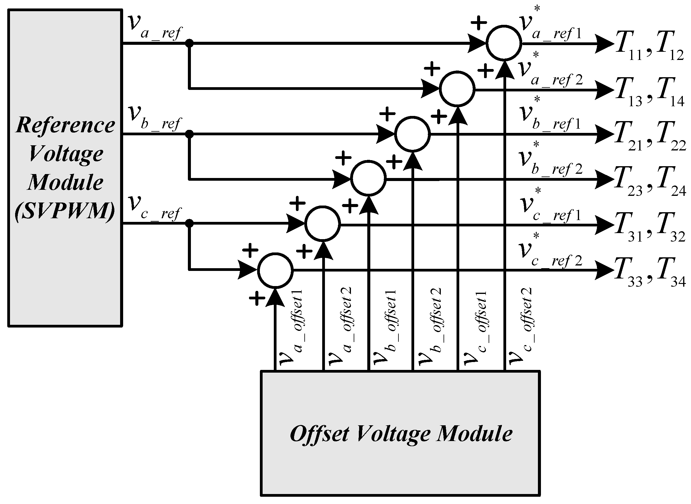
Figure 11 shows a control block diagram of the proposed ZDPWM technique based on previous illustration. As shown on the figure, it can be easily implemented based on the SVPWM technique.
However, since this method determines the offset of reference voltage according to the polarity of the phase current, unexpected distortion may occur if the delay occurs in the analog-to-digital converter (ADC) modules that senses the phase current. Therefore, in this paper, simple phase delay modeling was performed, and it was applied to the proposed ZDPWM method.
4. Phase Delay Modeling and Compensation Method
In this section we describe the problems that can arise when the proposed ZDPWM technique is actually implemented and how to optimize it.
Figure 12 shows the delay in sampling data caused by the ADC module in MCU. Since the sampling period of ADC modules is determined using the interrupt of the PWM modules in MCU, the initiation of the ADC for real-time data sampling is associated with the switching period, as shown in
Figure 12. The ADC modules which sense the current needs more than a certain amount of time to converter analog-to-digital data. Therefore, the phase current data are not immediately converted at the beginning of the sampling, and the data sampled at the previous time is used at the start of the next sampling. The sampled phase current is calculated as the lagging current relative to the real current and, consequently, the current controller or voltage controller of the inverter is operated through these sampled current data.
When the conventional PWM is used, it does not significantly affect switching operation even if it is sensed as a lagging current, because the delayed phase is compensated by using the d-axis current control. However, in the case of the proposed ZDPWM, because the phase of voltage and current are shifted by the sampling delay, it causes a delayed transition of the operation section. This delay of section transition delays the recognition of the zero-crossing of the phase current and causes distortion of the phase current. This delay of section transition also cannot be improved by only the d-axis control used in the conventional SPWM, SVPWM method. Therefore, the sampling delay should be improved to have the same phase with real current for the ideal operation of the proposed ZDPWM method.
The sampling delay
tdelay can be calculated by Equation (9) as:
where
fsw is the switching frequency of the inverter. The relation formula both the delay angle of phase current, which is output AC phase, and the sampling delay are calculated through proportional trigonometric equation as follows:
In Equation (10),
fref is the frequency of the reference voltage. In this paper, we propose the sampling delay compensation method through phase angle of d-q transformation using the delay angle which is calculated from the Equation (11) as:
The delayed phase current through sampling can be defined as follows:
Equation (12) can be expressed as a d-q axis current using the d-q transformation as follows:
In general, the phase angle which is used in d-q transformation is obtained by phase locked loop (PLL). T(0) and R(θ) are transfer matrix of the Park transformation and Clark Transformation. As shown in the Equation (13), finally, the current of d and q axis does not affect the sampling delay of the ADC modules.
Therefore, to prevent the phase delay caused by the sampling delay, as shown in Equation (14), the delayed phase angle obtained by Equation (11) is compensated when performing the reverse d-q transformation as:
Figure 13 shows a flowchart to compensate for the phase angle delay of the phase current. When sensing the current, as shown in
Figure 13, the phase angle of the current is delayed by the sampling delay. This delayed current is converted to a synchronous reference frame via d-q transformation, and harmonics within this value are removed by digital filters such as low pass filter. Then, the values of these converted synchronous reference frame are converted to a stationary reference frame again using the compensated phase angle shown in the Equation (14) via reverse d-q transformation. Therefore, the proposed ZDPWM method can use the phase current, which is not delayed, to calculate the offset voltage. The phase angle used in this time is compensated as much as it is delayed.
5. Simulation and Experimental Results
In order to verify the principle and feasibility of the proposed ZDPWM method, a simulation was developed using the PSIM software program. The simulation schematic in which the three-level NPC VSI back-to-back system is illustrated in
Figure 14. The systems parameters of the simulation are shown in
Table 3.
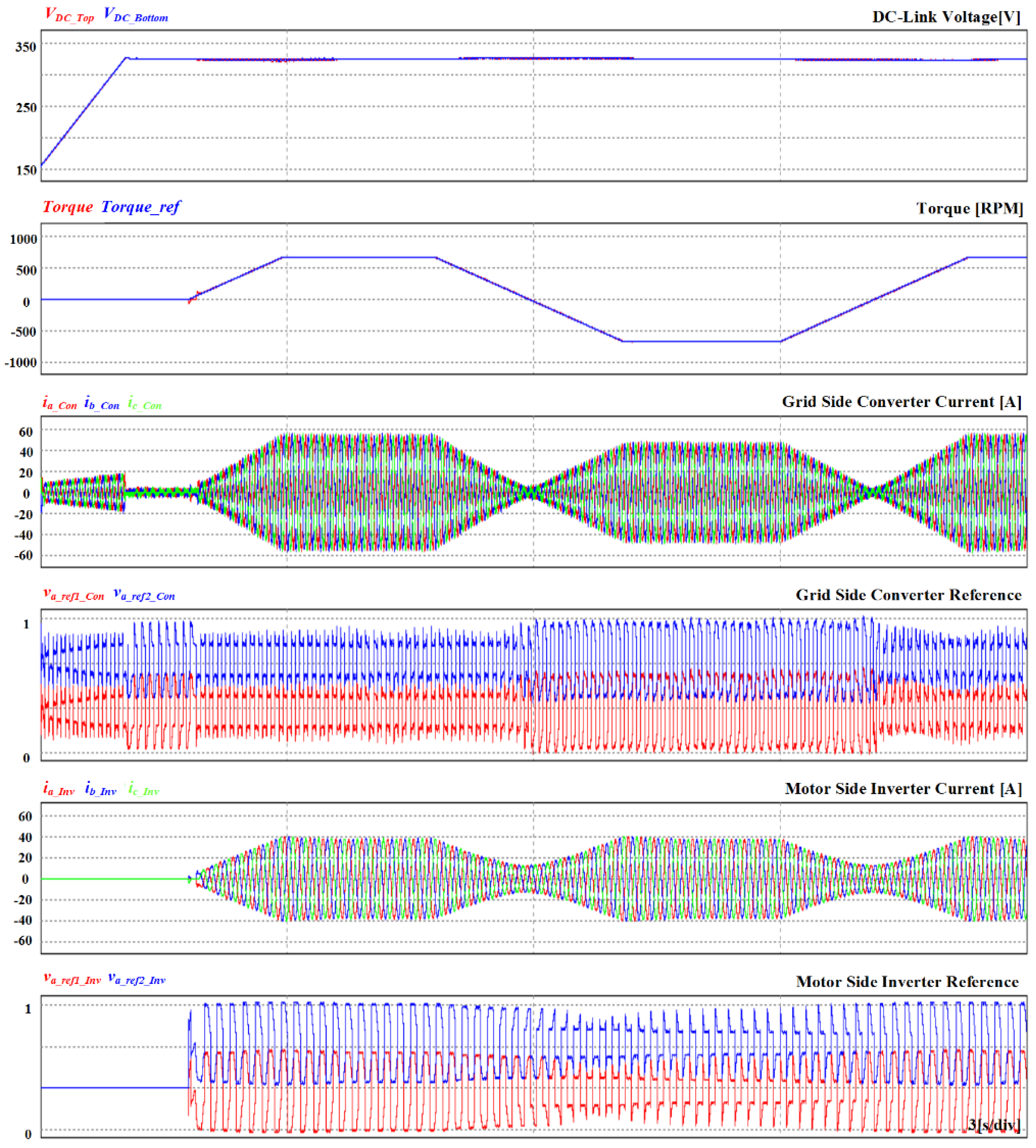
Figure 15 shows the results of a permanent magnet synchronous motor (PMSG) torque control simulation using a conventional SVPWM with dead time. When the control starts, the grid side inverter operates as a converter to perform voltage control. After reaching the normal state, the torque command is applied to the load side inverter at 0 → 670 (Nm) → −670 (Nm) → 670 (Nm). From the top, it shows dc-link voltage, torque, grid side measured current, grid side reference voltages, and current and reference voltages to motor load. In order to figure out the dead-time effect, grid side current, LCL filter current, and motor current are shown on
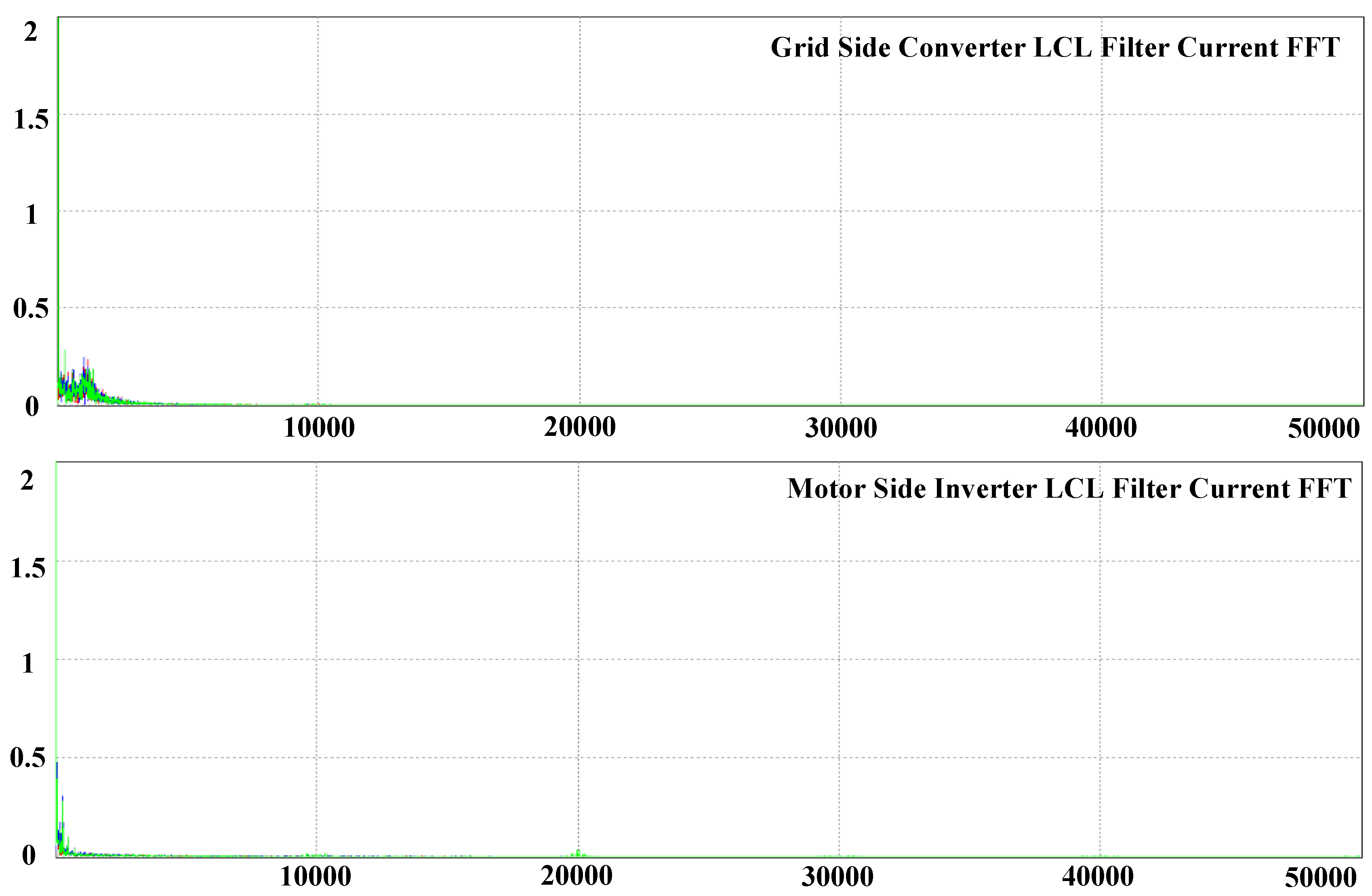
Figure 16. As previously explained, dead time is applied to prevent a short circuit accident, but it causes current distortion. This distortion appears in the form of low-order harmonics when performing fast Fourier transform (FFT) analysis, as shown in
Figure 17.
Figure 18 shows the simulation results when applying the proposed ZDPWM in the same conditions without dead time as the previous SVPWM. The applied load is the same as the previous condition 0 → 670 (Nm) → −670 (Nm) → 670 (Nm]). As shown in
Figure 19, the proposed ZDPWM does not use dead time, and current distortion cannot be seen caused by dead-time effect of the current in the grid side, the LCL filter, and the load motor. Thus, the FFT analysis, as shown in
Figure 20, indicate that the low-order harmonics produced by dead time are significantly reduced as compared with SVPWM.
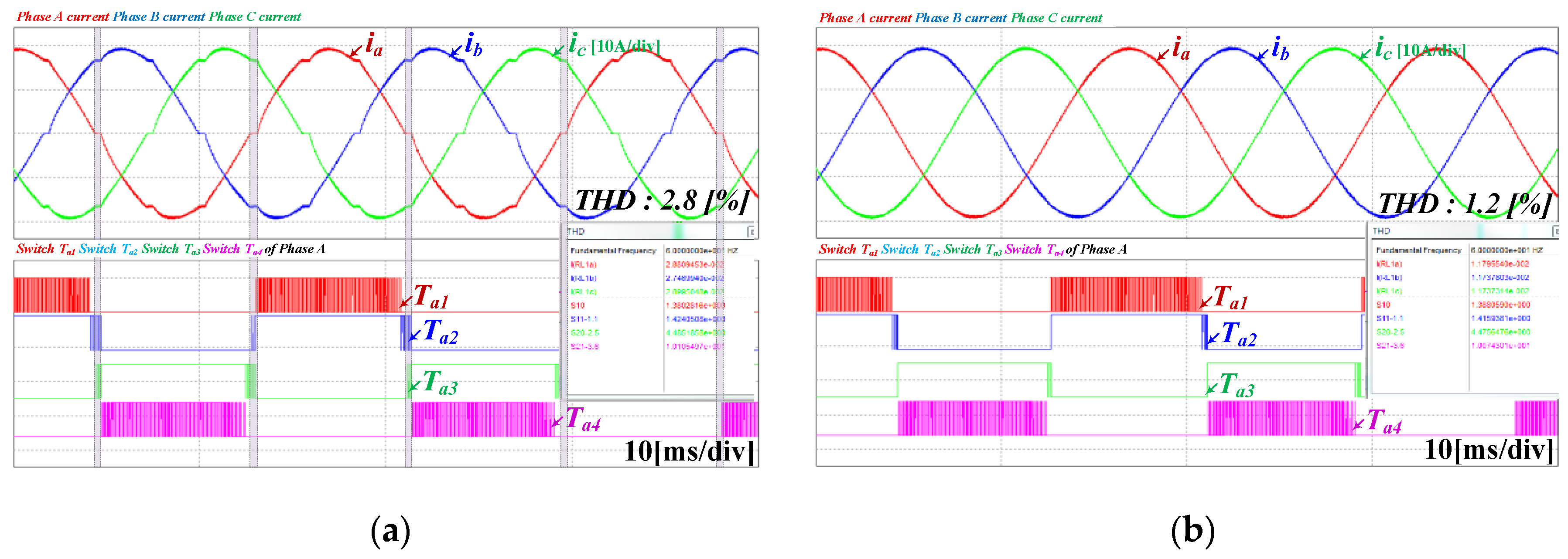
Figure 21 shows the comparison simulation result of the conventional SVPWM and proposed ZDPWM method. As previously mentioned, when using the conventional SVPWM method, dead time increases the distortion in the phase current, which causes an increase in the THD. However, the proposed ZDPWM method does not require dead time because it does not perform a complementary operation, as shown in
Figure 21, and therefore it reduces the distortion in the phase current. Consequently, when using the conventional SVPWM method with dead time, the THD of the current is about 2.4%, but the THD of the current is about 1.2% when using the proposed method.
Figure 22 also shows the simulation waveforms before and after applying proposed ZDPWM with sampling delay compensation. We can see that the proposed ZDPWM method is more distorted by the sampling delay of the phase current at the section where it is transmitted, as shown in
Figure 22a. At this time, the THD of current is about 2.8% and is higher than the conventional SVPWM method.
Figure 22b shows that by compensating the delay, the distortion caused by the delay is reduced.
In this case, the compensated phase angle, which is calculated by using the Equation (11), is shown in
Figure 23. Therefore, although the phase of the sensed current is delayed more than the real current, the phase current used in the proposed ZDPWM method has the same phase as the real current because delay is compensated during the reverse d-q transformation.
Simulation results of three methods are summarized as
Table 4. The THD characteristics of the conventional SVPWM, proposed ZDPWM without delay compensation and proposed ZDPWM with delay compensation are 2.4%, 2.8%, 1.2% respectively. As a result, proposed ZDPWM with delay compensation is the best method to improve current distortion of a three-level NPC inverter.
In addition, in the NPC topology, in this paper, voltage unbalancing occurs in the dc-link due to load condition, difference in charging/discharging status according to current direction, etc. Therefore, as illustrated in [
31,
32], voltage balancing in dc-link is generally achieved by applying offset voltage to the PWM output from SVPWM, PSPWM, or LSPWM. In this paper, we also applied offset voltage to compensate dc-link unbalancing at the output end of ZDPWM, and conducted simulation by applying offset voltage the same as the conventional SVPWM.
Figure 24 and
Figure 25 show the simulation results applying SVPWM and the proposed ZDPWM in a three-level inverter, respectively. As shown in the figure, all applications in this paper perform voltage balance control, and therefore the dc-link voltage imbalance in the upper/lower capacitors does not occur.
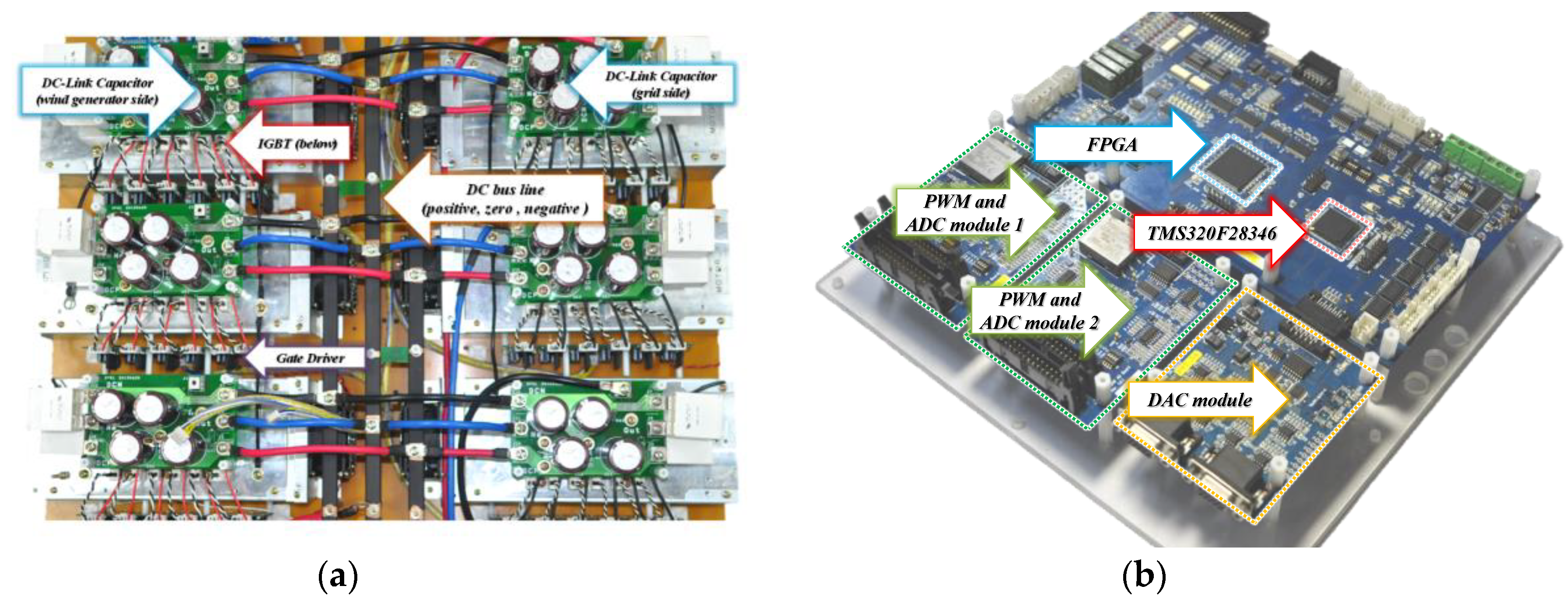
An experiment was performed to verify the feasibility of the proposed ZDPWM method applied in a three-level NPC VSI. The configurations of the experimental system and power stacks are as follows in
Figure 26 and
Figure 27.
The controller is implemented on TMS320F28346 and that of a floating point microcontroller unit at 300 MHz rate frequency. The switching and sampling frequency is 10 kHz. The power is supplied to the three-level NPC inverter through the three-level NPC PWM converter.
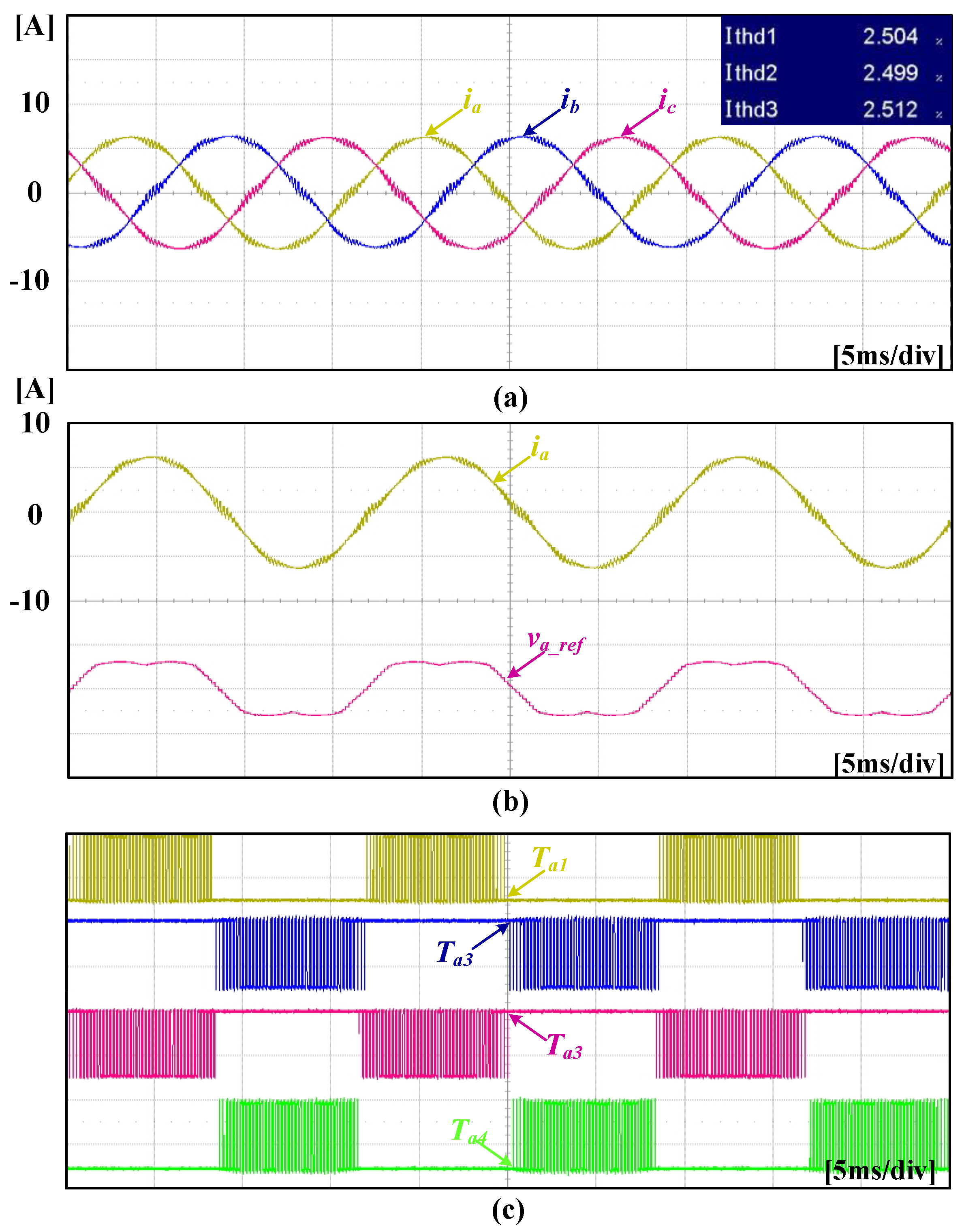
Figure 28a shows the output phase current waveforms of each phase when the conventional SVPWM method is used in a three-level NPC VSI. In this experiment, the dead time was 5 us. As shown in
Figure 28, we can see that dead time causes the distortion of the output current and, in particular, large distortion of the current, at zero crossing points.
Figure 28b shows the phase A output current and reference voltage waveform, and the switching signal according to the reference voltage is generated, as shown in
Figure 28c. As a result, it can be seen that the THD of the output current has deteriorated to about 2.5% due to the dead time.
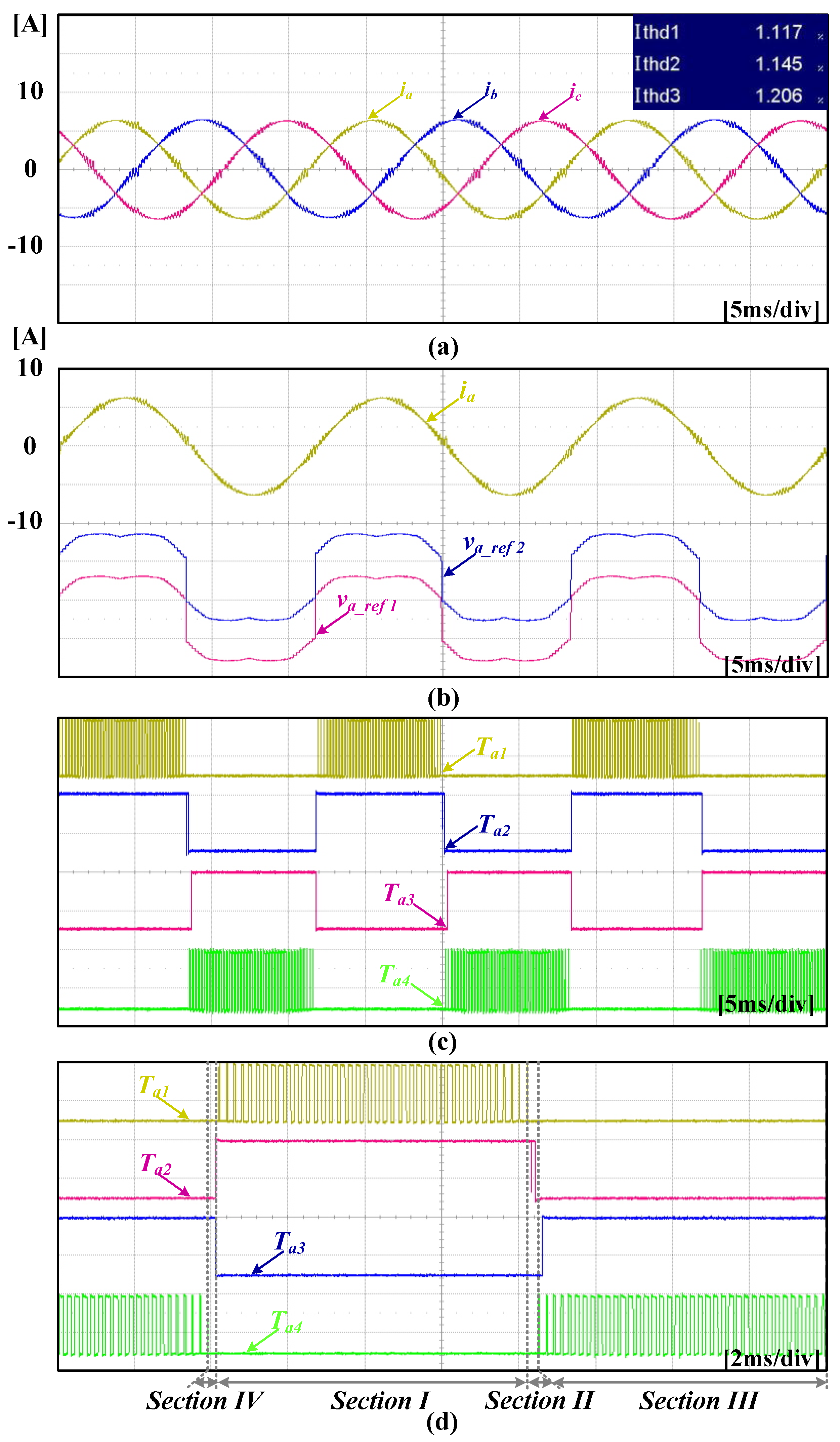
Figure 29a shows the output phase current waveforms of each phase when the proposed ZDPWM method with delay compensation is used in a three-level NPC VSI. In this experiment, the dead time was not applied.
Figure 29b shows the phase A output current and reference voltage waveform.
Figure 29c shows the switching signal generated by two reference voltage which are adding the offset voltage to reference voltage. In the conventional SVPWM method, each switching signal is generated by applying the dead time in order to perform the complementary operation and prevent the short circuit, but in the proposed ZDPWM method, it is possible to verify that the switches
Ta1 and
Ta3, and the switches
Ta2 and
Ta4 do not perform the complementary operation, as shown
Figure 29d. As a result, we can see that the THD of the output current is about 1.2% better than the conventional SVPWM method by about 1.3%.
6. Conclusions
In this paper, we have proposed the ZDPWM method with compensation of the sampling delay in three-level NPC VSI. It can reduce the current distortion caused by the dead time and it is easy to implement.
We discovered that complementary switching operation of the NPC VSI was the reason dead time was needed and we described how to operate the NPC VSI without dead time. In addition, the sampling delay modeling was described to compensate the delay of the phase current.
In this paper, a simulation and an experiment were performed and presented to verify the proposed ZDPWM method as well as their feasibility. From them, the proposed method resulted in better performance of lower current harmonic distortion.
From the simulation result, the current regulated by conventional SVPWM has a THD of about 2.4%, the current regulated by proposed ZDPWM without sampling delay compensation has a THD of about 2.8%, and the current regulated by proposed ZDPWM with sampling delay compensation has a THD of about 1.2%. Additionally, in experimental result shows that the current regulated by proposed ZDPWM without sampling delay compensation has a THD of about 2.5% and the current regulated by proposed ZDPWM with sampling delay compensation has a THD of about 1.2%, similar to the simulation result. These results indicate that THD can be significantly reduced by the proposed method. As a result, the proposed ZDPWM is a good PWM strategy for three-level NPC VSI systems.


