1. Introduction
1.1. Background
The verification of designs at the software, hardware and firmware level is one of the most important tasks to assure the correct functionality of a designed application. This can be especially critical in fields where a functional failure is costly in terms of economy or risk to human life, such as biomedical and aerospace industries.
At the firmware (also called gateware) level, there are multiple ways to verify the behaviour of a circuit, from the basic use of simulation tools to simulate specific parts of a design [
1], or using these simulation tools following standard verification methodologies, such as UVM [
2] or UVVM [
3], to applying formal verification [
4].
Simulation-based approaches allow the user to monitor the behaviour of his/her circuit when faced with given stimuli. This is also known as functional verification. When the complexity of the designs grows, testbenches also become more complex and thus require more time to be developed. For this reason, there is a high interest in the industry to reuse code for testbenches and streamlining the verification process. UVM and UVVM are simulation methodologies to describe testbenches and its components in a generic way, so that they can be reused for many different projects and allow automatic testing.
Formal methods are capable of proving that the properties of a given design hold, under specific conditions (such as inputs within an expected sequence of values), using mathematical methods, without the need to create complex testbenches.
As the complexity of the design increases, as can happen in the integration between software and hardware, the verification becomes more complex and therefore requires the use of more sophisticated tools to detect and correct errors in the application or design to be verified.
1.2. Problem of Interest
Nowadays, there are different tools to perform verification, such as Vivado Simulator [
5] or Questa Advanced Simulator [
6] for HDL simulation, which typically require the purchase of expensive licenses. Recently, free and open source software tools have emerged that are capable of simulating HDL designs with accuracy, speed and adherence to the HDL Standards that can rival many of the commercial tools (particularly the ones integrated with the software provided by FPGA vendors). A revision of what can be done with these free and open source tools can be found in [
7].
Basic simulation, without following any functional verification methodologies, has the advantage of requiring little engineering effort at first, but it does not scale well when testing complex modules or using complicated input sequences, requiring more and more engineer effort as complexity increases. For this reason, it is seldom used to simulate complete designs, but is instead used by the design engineers to make some quick verification of the most basic functionality of a module. When verification metrics are used, this verification method typically obtains poor results.
Functional verification methodologies improve on what can be done with simulation, by structuring testbenches so that engineering efforts are distributed between different testbench submodules which may also be reused. The main drawback of these methodologies is their steep learning curve: for example, if a VHDL designer wants to use UVM to verify a design, he or she must first learn Verilog, SystemVerilog and object-oriented programming, and then learn the UVM. Furthermore, the commercial simulators that support the versions of the HDL standards that these methodologies need (SystemVerilog in the case of UVM, and VHDL-2008 in the case of UVVM) are not distributed with the FPGA vendor tools and must be purchased separately. This makes designers, especially the ones whose target is an FPGA, not have the economic or time budget to use them. The reason being that these methodologies are mainly tailored for designs that are going to silicon, but designs whose target device is an FPGA (which would gain confidence if using these methodologies) often find that the designers do not need all the verification capabilities and their time/effort budget is not sufficient to warrant the use of these methodologies.
Formal methods are notably powerful for demonstrating circuit properties in small-to-medium design blocks. Due to the heavy mathematical load of these methods and the change in mindset that the verification engineer needs to undertake in order to use them, they typically require special training. As the complexity of the mathematical proofs increases exponentially with design complexity, these methods do not lend themselves well to checking full designs. In some cases, the formal models of the full designs may be simplified in order to reduce calculation time, which could create verification gaps if not done correctly.
Apart from the verification methods chosen, projects where integration between hardware, software and firmware is required often suffer from delays, which may risk the final project closure on time. A missing hardware or firmware part may block the progress of the software part and vice versa, resulting in a delay of the global project. The integration with external software is subject to the capabilities of proprietary simulators, and the users may be in a situation where they want to access a feature that is not covered by their current licenses. Furthermore, simulators that are provided with the typical FPGA vendor tools, which are the ones that the majority of users know how to use, do not support the VHDL or Verilog capabilities that these modern verification methodologies require. It would be desirable to have a verification environment whose capabilities were not limited by proprietary licenses, while being easy to use to verify a complex design where the integration of software and hardware is required.
1.3. Literature Survey
In the existing literature, there are several methods and tools to perform the verification of different kinds of designs or circuits. They can be classified into two categories: functional verification and formal verification.
Functional verification based on simulation can be done by stimulating the design under test with ad hoc test benches using a software simulation tool. Commercial simulation tools are used in [
8], where genetic algorithms are used to define input patterns, which are fed to a VHDL simulator to drive the system to configurations that increase code coverage, improving the capabilities of the verification by simulation technique. In [
9], the co-simulation of hardware and software for a system-on-chip is achieved by running the software part in a simulated hardware model. Co-verification allows verifying the complete final system, thus avoiding software development time delays due to missing hardware or mismatches between hardware architecture and software application.
Other approaches for functional verification, such as [
10,
11], use the standard methodologies, such as UVM or UVVM, to verify their designs. A recent study in FPGA verification trends in industry can be found in [
12]. On the other hand, in academia, there seems to be a lower penetration of functional verification methodologies, and specific verification efforts are typically not mentioned in publications, except the ones that directly focus on verification [
13,
14,
15,
16]. Some researchers, such as [
17], propose their own methodologies with reusable modules, resulting in testbench architectures similar to (but not compatible with) the standard methodologies.
If a higher level of confidence is needed, formal verification methodologies may be applied. This technique allows to mathematically prove or disprove properties of the circuit, without using simulations. A popular use is to check that specific error conditions will never occur in a module, given a set of restrictions in its inputs. For some circuits, another use case could be to compare the equivalence between the design under verification and a reference model that behaves as desired. A survey of techniques for formal verification for co-verification is collected in [
18].
When the complexity of the designs increases, formal verification techniques are more difficult to apply. In these cases, approaches that combine different verification methodologies can be useful. Ref. [
19,
20] combine techniques of simulation and formal verification to reach a compromise between confidence and complexity.
1.4. Scope and Contribution of This Paper
This paper presents the design and development of a co-verification environment with both software and firmware components that allows to verify the functionality of an FPGA application that communicates with a software that runs on a PC, all using open source tools.
Although approaches like [
9] also perform co-verification techniques, there is not a single one among the above proposed that performs co-verification where the software and hardware parts interact, but are independent of each other. In the case of [
9], the software runs inside the simulated hardware, while in the proposed approach, the software runs on a PC and communicates with a firmware application running on an FPGA.
The proposed verification approach has a lower learning curve than standard methodologies, since it does not require learning a different language or constructing a very complex testbench in terms of transactions, drivers, monitors and agents.
Another advantage of the proposed approach compared to the rest found in the literature is the use of open source tools, which avoids licensing requirements that limit the capabilities of the software, allowing full access to the tool for the user.
1.5. Organization of the Paper
The paper is structured as follows:
Section 2 describes the design under co-verification and how to construct the co-verification environment.
Section 3 describes the test procedure. Experimental results obtained using the co-verification environment are shown in
Section 4. Lastly, the discussion and conclusions are presented in
Section 5.
1.6. Graphical Abstract
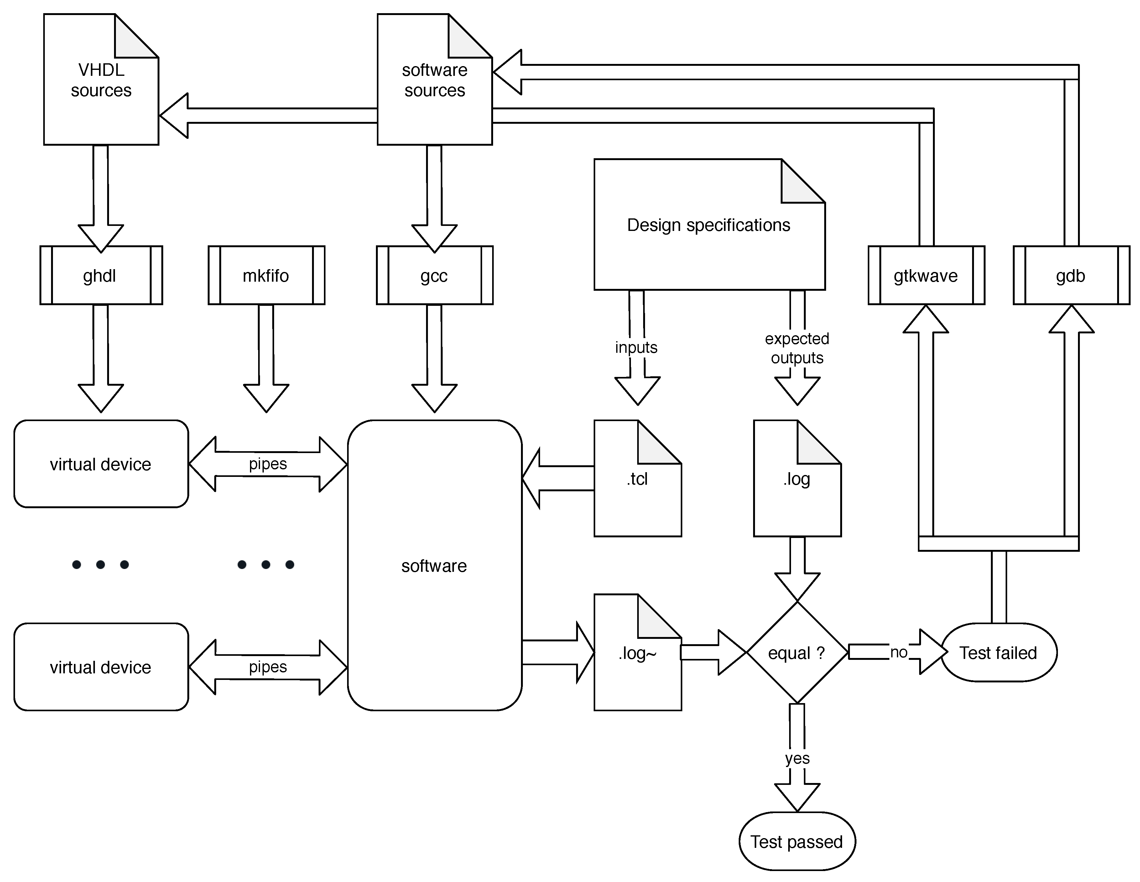
Figure 1 summarizes the proposed approach, test procedure and involved files and tools, which will be explained in the following sections.
2. Co-Verification Environment
2.1. Design under Co-Verification: The FTU-VEGAS System
The design under co-verification is the system logic of the FTU-VEGAS system, an FPGA-based fault injection platform developed by Universidad de Sevilla for the European H2020 project VEGAS. This fault injection platform is based on its previous version FT-Unshades2 [
21], which allows to inject single event upsets (SEUs) on the user logic and configuration bits of an FPGA.
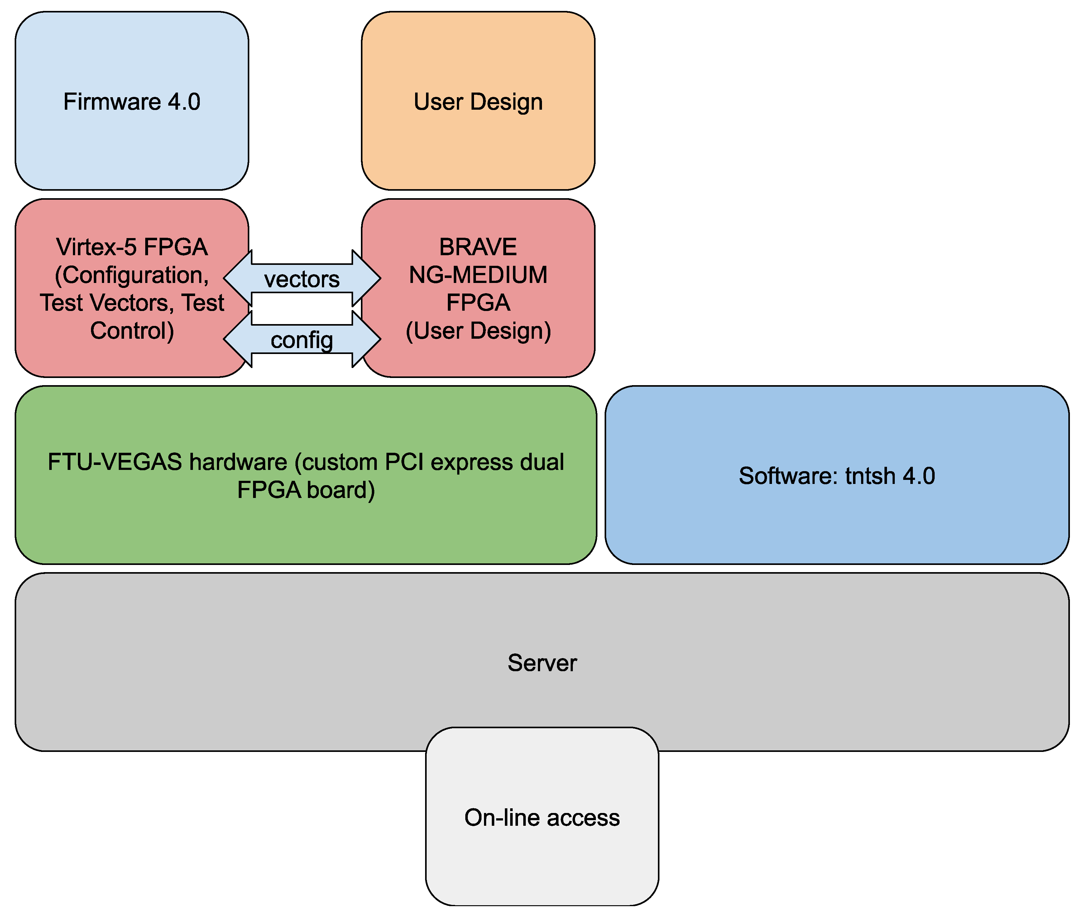
The architecture of the complete system can be seen in
Figure 2. In the absence of any specific verification efforts, all the different elements of the platform must be available in order to test and verify the system logic, which is implemented in the software and firmware.
The elements that compose the design are described in the following sections.
2.1.1. The Hardware Device
The hardware side of the system is a custom PCI express dual-FPGA board. The two FPGAs are a Xilinx Virtex-5 and a NanoXplore BRAVE NG-MEDIUM. The first FPGA is called the Service FPGA, and the second one is called the Target FPGA. The purpose of the system is to study the behaviour under radiation-induced faults of the Target FPGA, which can be configured with different user designs. The Service FPGA must then contain all the necessary firmware to control the fault injection testing and associated on-board hardware: buses, communications, memory, etc. The hardware device also includes two on-board memories and a PCI express port to connect to a PC. The design and production of this hardware device consisting of a custom PCB with these two FPGAs require a considerable fraction of the project time, resulting in a bottleneck in the development process.
2.1.2. The FPGA Firmware
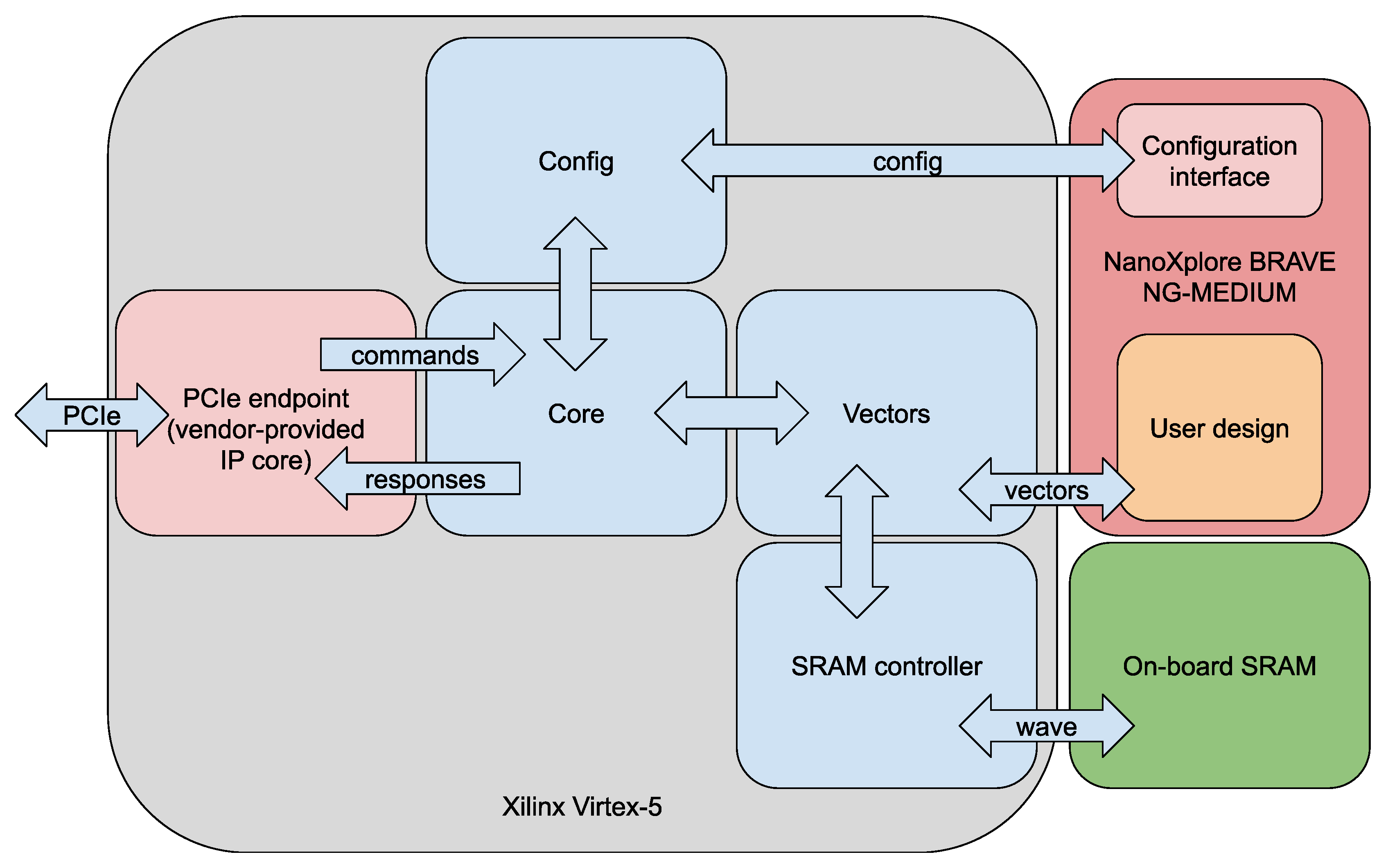
The firmware that runs in the Service FPGA is responsible for the low-level management of the fault injection testing and all on-board hardware. The different modules of the firmware exchange data using custom-made stream blocks that allow managing a flow of data whose width may change. The architecture of the firmware is shown in
Figure 3, which also shows other on-board components that directly interact with it.
The main functional blocks in the firmware are:
Core: decodes commands from software, manages the other modules and sends responses to software.
Config: manages the configuration interface of the Target FPGA.
Vectors: manages the feeding of test vectors (stimuli and clock) for the user design. Communicates with the SRAM controller to store the input and output vectors in order to minimize communications with the software.
SRAM controller: manages data transfer with one of the on-board SRAMs.
2.1.3. The Computer Software
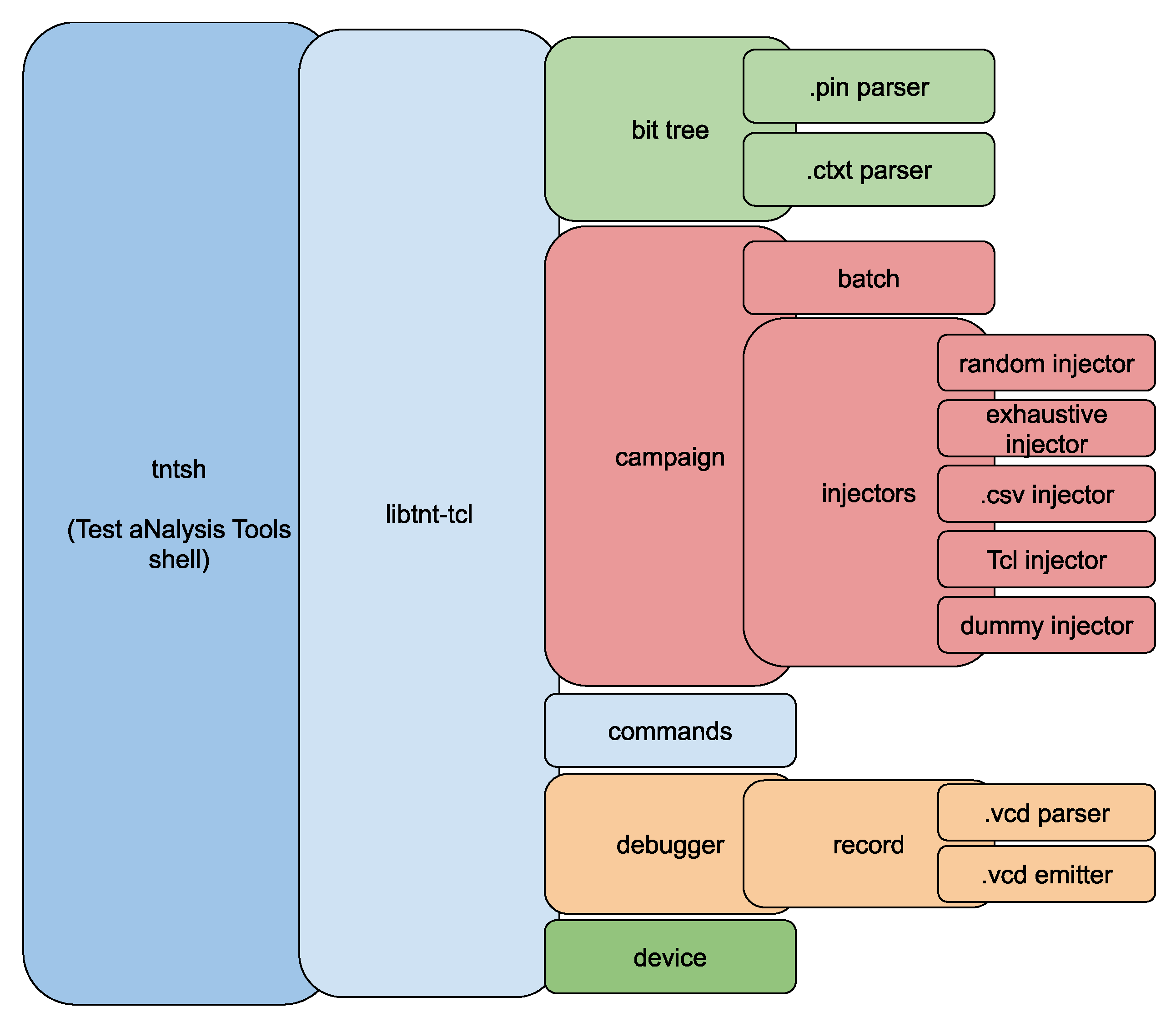
The software runs on a computer to which the hardware is connected and interfaces with both the hardware and firmware of the system, interpreting and executing the user commands which can be read either from an interactive shell or from a script file. Most of the functionalities of the software require interacting with the firmware that is supported by the hardware. The software is called tntsh (test analysis tools shell), and its architecture is shown in
Figure 4.
The main functional modules of the software are:
tntsh: a tcl shell that interprets the user commands and can be used in batch mode.
libtnt-tcl: extends the tntsh functionalities by wrapping the C/C++ API of the internal modules, so that they can be accessed through the tcl shell.
bit tree: creates an internal representation of the design hierarchy. The .pin files are I/O pin representations and the .ctxt files are internal design representations.
campaign: the top-level implementation of the fault injection tests. Different injection schemas may be used, and campaigns can be run in batch mode.
commands: header file with the command codes
debugger: allows single-step execution, interactive debugging and reading and writing .vcd files with the inputs and outputs of the design under test. The record submodule manages an internal compressed I/O vector format.
device: manages the communications with the FTU-VEGAS device.
2.2. Developing the Co-Verification Environment
2.2.1. Traditional Testing
Unit tests can be performed at all levels by building a test environment for every module developed, both at firmware and software source levels. Due to the complexity of the system, these unit tests may only cover small parts of the complete functionality. Many, if not most, of the functionalities of all system elements require the system to be at least partially complete, to cover all the functionality that depends on the interactions between the different system elements.
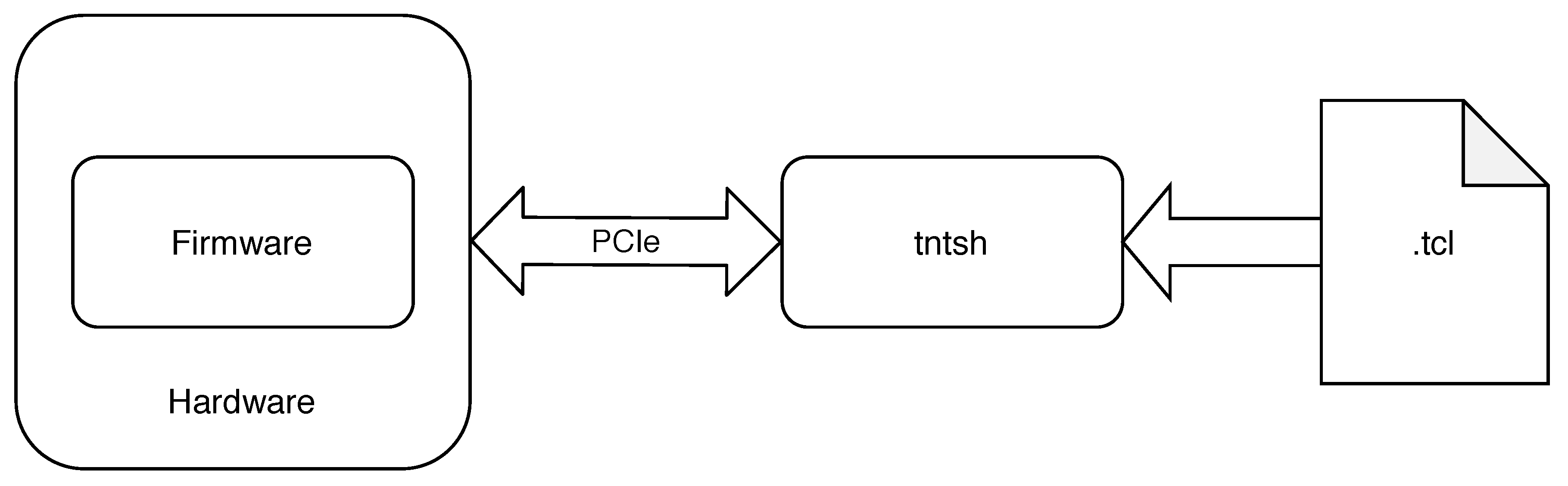
If no specific verification actions are taken, integration tests can only be run if we have the complete system, as shown in
Figure 5. Waiting for the complete system to be available in order to begin a thorough testing of the system logic increases risk and may introduce delays in the project.
The integration tests use the Tcl API provided by tntsh to run a test script and compare the output with a model that is sometimes hand made, sometimes generated with an independent script, and sometimes generated with a previous version of the system and checked for errors. Unfortunately, they cannot be executed without the hardware.
2.2.2. Testing Software with No Hardware or Firmware
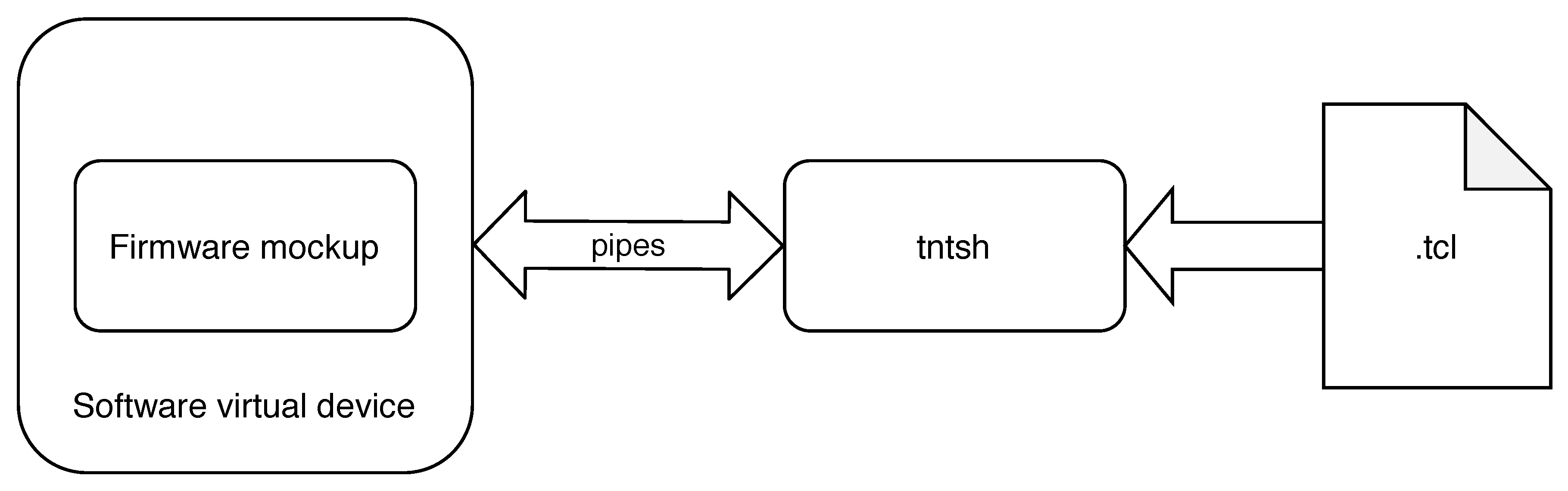
At some point in the development process, it was noticed that the software was getting ahead of the rest of the project, but could not be tested beyond the most basic unit tests because there was no platform to do so. The solution is then to provide a platform that does not require the same resources that the hardware does, as can be seen in
Figure 6.
Since the communication protocol between software and firmware had been specified, it was possible to write a software module that behaved just like the firmware and hardware would. It could not be connected to a PCI express device, but since a PCI express device connected to a unix or unix-like server can become a device file in userspace, the presence of the device can be emulated by a pair of named pipes that connect the software and our virtual device.
The software virtual device is a computer program that completes the following tasks:
Open the read and write pipes that connect it to the tntsh software.
While the pipes exist:
- -
Read 1 byte from the input pipe.
- -
Decode the read byte to obtain the command sent by tntsh.
- -
Execute the command, reading from the input pipe any data needed.
- -
Send the expected response to the output pipe.
Exit cleanly, closing any open files and releasing any reserved memory.
If the software is well structured, multiple files can be shared between the software and the software virtual device, such as the header file with the command codes, communication protocol details, and internal data structures, which eases the construction of the software virtual device. Reusing these files is a tradeoff between development speed and verification capability.
The software virtual device has many limitations: it does not actually simulate the Target FPGA; instead, it has a table where the bitstreams are copied and the values of individual bits can be queried and changed. For these reasons, only a subset of the software functions can be meaningfully tested. The simulation of the functionality inside the Service FPGA is not cycle-accurate, since no HDL code is being used. The emulation of the user design is also missing, since there is no simulation of any HDL. It does, however, handle all possible error conditions and returns the appropriate codes. Examples of these are sanity checks, such as reporting an error if the user tries to perform a single clock step without any vectors previously loaded. While this solution is interesting to test a number of software functions that need some interaction with the device, it cannot be used to verify any of the VHDL code of the firmware, since it is not involved in these tests. When enough firmware code is available, a firmware virtual device becomes preferable, making the software virtual device obsolete except for functional comparison purposes.
2.2.3. Testing Software and Firmware with No Hardware
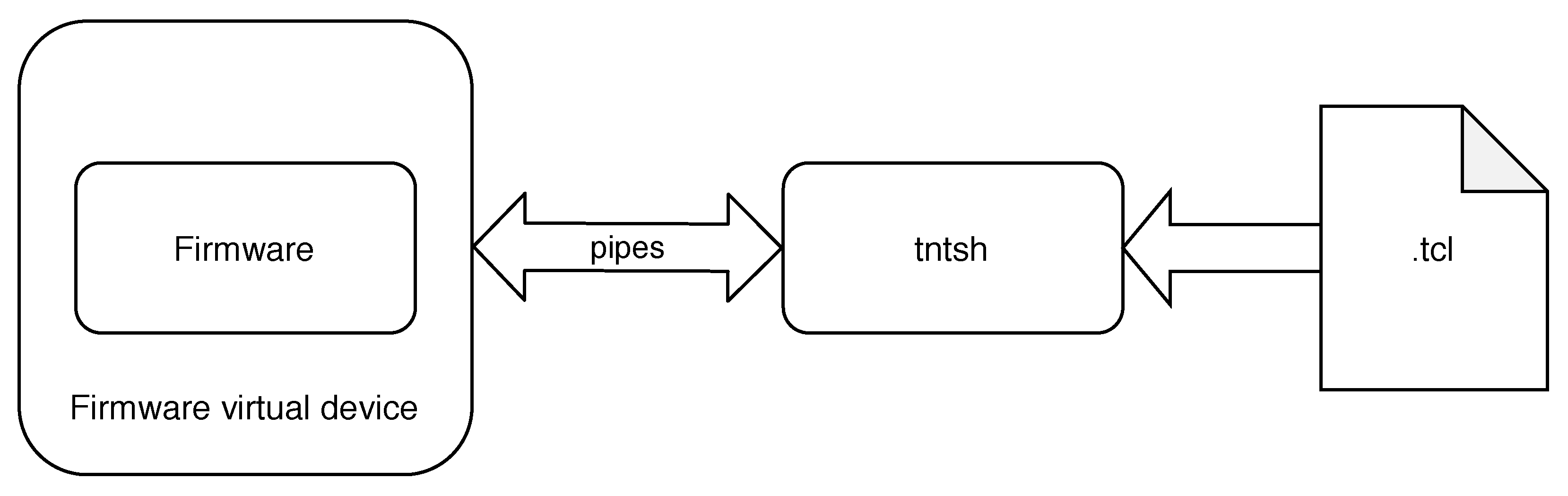
As development advanced, the firmware for the Service FPGA grew, as did the required integration tests, but the development of the hardware lagged behind producing yet another bottleneck. With the software virtual device in mind, the same principles can be applied to remove the need for actual hardware in these tests. To achieve this, it would be desirable to have a simulation of the firmware HDL code that could manage the communication with the unix pipes. The components required to perform the integration tests in this case are shown in
Figure 7.
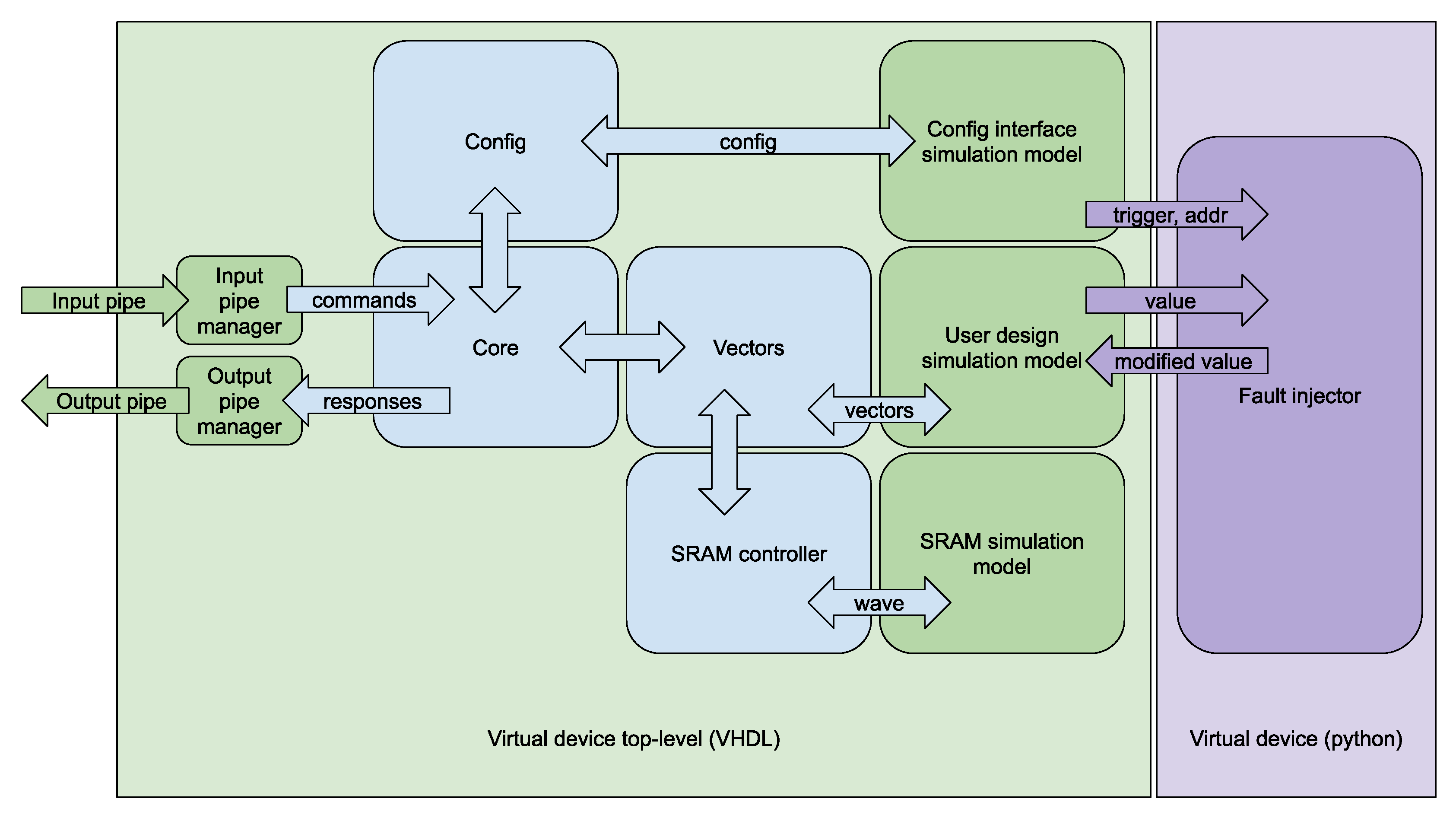
In order to construct the firmware virtual device, a number of additions have been made to the firmware architecture. The modified architecture is shown on
Figure 8, and it includes the following new elements:
Configuration interface simulation model: a simple model of the configuration memory of the Target FPGA that allows to write and read data from it.
User design simulation model: instances one of a number of different possible designs.
SRAM simulation model: models the on-board SRAM. Allows to store and retrieve data.
Virtual device top-level (VHDL): a wrapper that instances the needed firmware modules and simulation models, and manages communication between the software shell (tntsh) and the instantiated firmware through a pair of pipes. This top level implements a VHDL generic that allows to select the user design and is passed to the user design simulation model.
Virtual device (Python): a small script that modifies signal values in the user design when it detects write operations in the configuration interface simulation model. The Python script uses the cocotb coroutine cosimulation framework [
22] in order to perform the fault injections.
Compiling the first four modules with the rest of the firmware code, with GHDL [
23], results in an executable file: the firmware virtual device. In case of testing any system features that need fault injection, the relevant environment variables must be set or passed so that the Python script is executed with the virtual device.
The firmware virtual device solves the drawbacks that the software virtual device had: it includes a simulation model of the Target FPGA with fault injection capabilities, the simulation is cycle-accurate, and the user designs in the Target FPGA can be emulated. There is no possible verification gap due to code reuse, since all the code of the firmware virtual device is written in a different language than the software. The tradeoff is that the firmware virtual device requires longer execution times, since the VHDL simulation is more complex than the execution of the software virtual device.
3. Test Procedure
3.1. Unit Tests
Before running the integration tests, it is always advisable to run all unit tests available. This saves time in case of an easier-to-detect error being inserted in the code, since it would not make sense to run the integration tests with erroneous code. The developed unit tests check the main functionalities of the different submodules of the system and have been automated using the GNU Make tool.
3.2. Integration Tests
3.2.1. Components
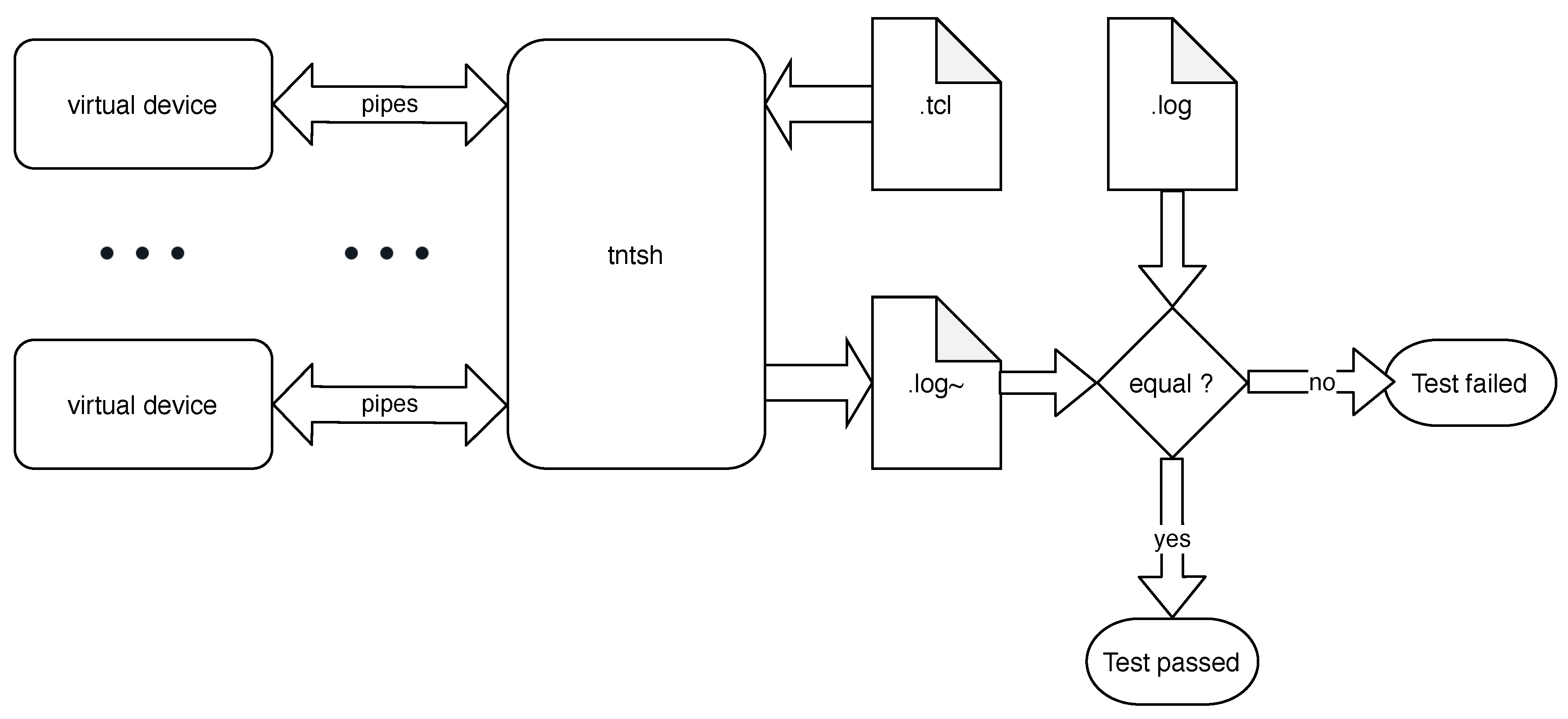
Figure 9 shows the different components that must interface for every integration test performed:
The software shell, which is the tntsh software of the project.
One or more virtual devices.
One pair of named pipes per virtual device.
A script that is executed in the shell (.tcl file).
A model output (.log) that is compared to the shell output (.log~).
3.2.2. Process
The procedure to run the tests is as follows:
Create n pairs of named pipes, where n is the number of devices required to run the test (typically 1, but more are needed when testing multi-device functionality). These pipes will be used for communication between the virtual devices and the software shell.
Launch n virtual devices, each one using a different pair of named pipes.
Execute the script in the software shell. The script is the one responsible for opening the virtual devices through the names of the pipes.
The output of the script is written to a file, e.g.,: testname.log~
When the software shell ends, the test environment must be cleaned: the processes for all virtual devices must be terminated and the named pipes used for communication must be removed. The Python part of the virtual device catches the SIGTERM unix signal in order to gracefully terminate the simulation, to avoid any possible data loss, such as code coverage files not being written.
Table 1 summarizes the test procedure, which has been automated through the use of the GNU Make tool, showing the tools used to obtain the required components and perform the tests. As soon as it becomes available, the use of the firmware virtual device is preferred to the software one.
3.2.3. Error Conditions
The test fails if one of the following conditions happen:
tntsh terminates with an error code or raises an exception.
The actual test output testname.log~ and expected test output testname.log do not match.
The test does not terminate (see below).
Otherwise, the test is assumed to have succeeded. A potential pitfall for this system is that an error in the virtual device can result in a test that never ends if the software keeps waiting for a response that will never come. This can happen if the virtual device gives a shorter response than expected or is caught in an endless loop itself. A timeout can be implemented at several levels to prevent this: it can be implicit in the software shell itself—only in debug mode, in our case—or it can be implemented in the scripts that manage the test. Furthermore, assertions can be added to both software and HDL implementations of the virtual device to detect the most probable failure conditions. If a new failure condition is detected as a result of executing a new test, new assertions can be added as needed.
3.2.4. Debugging
The software virtual device can be debugged with any software debugger such as gdb, simply launching the application with it. Having launched this process, the rest of the test proceeds as usual, and it can be interrupted at any time by the user.
The GHDL virtual devices can be made to export waveform data. This can be done by passing the --wave GHDL option to the firmware virtual device executable. The generated files can be viewed with the open source waveform analyzer tool gtkwave.
4. Experimental Results
The co-verification environment, with the firmware virtual device, has been used as a verification platform for the firmware and software parts of the FTU-VEGAS fault injection system. A set of unit tests was performed to check the correct functionality of each element of the firmware and software parts. Afterwards, integration tests were executed, in order of increasing complexity. For each test, a comparison between the expected output and the actual output has been performed to detect differences between them, thus allowing to find bugs in the system and fix them. In addition, several fault injection campaigns have been performed using the virtual device, obtaining results as expected. These fault injection campaigns are also a type of integration test, since performing fault injection campaigns is the intended use of the system under co-verification, and in order to perform them, most of the functionalities of the system have to be used.
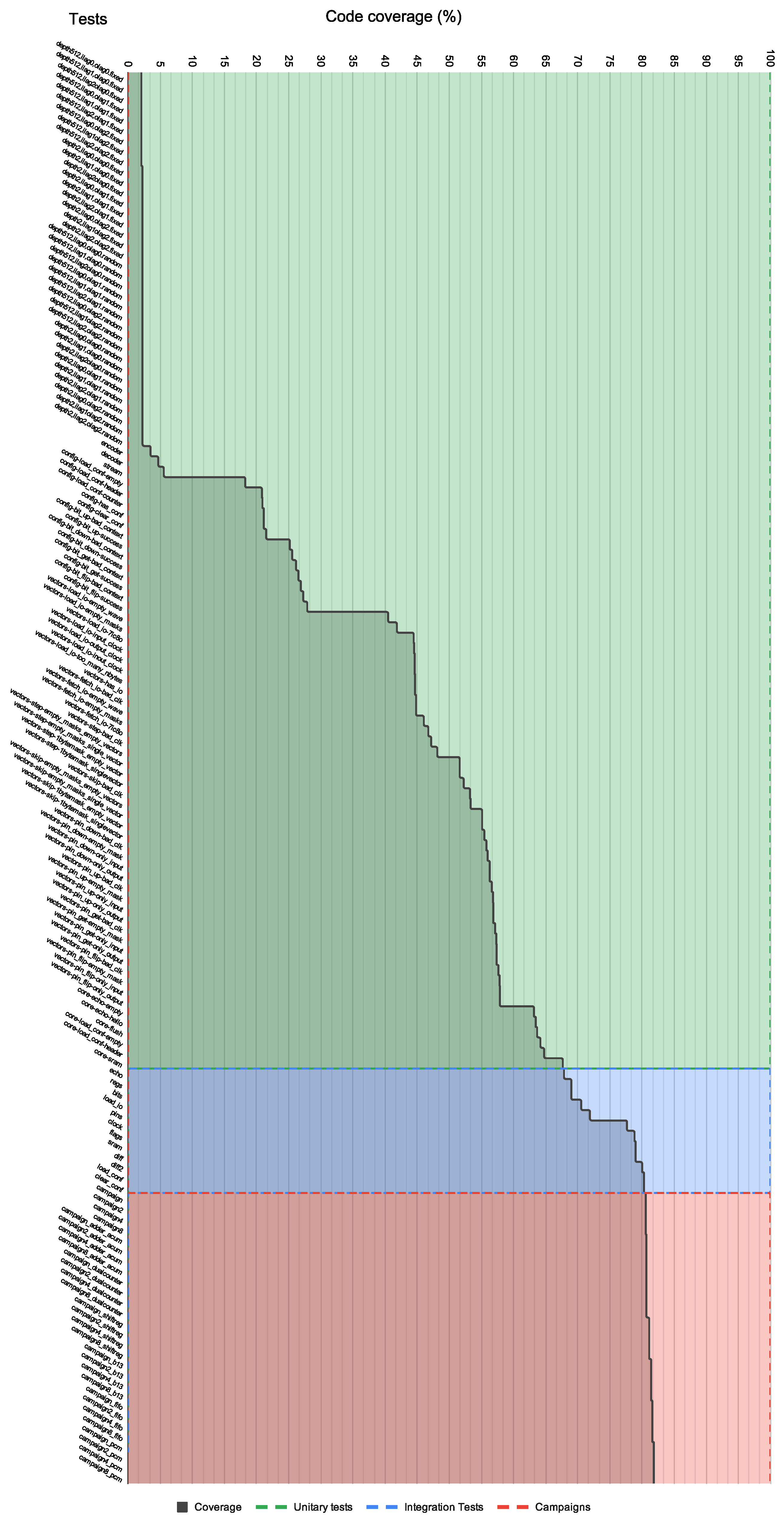
The code coverage metric has been obtained using GHDL and accumulatively measured after each test, so the increase in the metric with each new test can be measured. GHDL can generate line coverage metrics if compiled with the GCC backend.
Figure 10 shows how the code coverage metric improves with each added test, where the green area corresponds to unit tests, the blue area to non-campaign integration tests and the red area to the fault injection campaigns performed. The final code coverage reached is 82.97% of the source code, which is a large quantity considering that no actions have been taken specifically to increase the code coverage metric. Further increases in this metric could be achieved by identifying and analyzing the unreached code, in order to develop unit or integration tests specially tailored to hit the missed lines.
4.1. Firmware Unit Tests
The set of firmware unit tests executed is summarized in
Table 2,
Table 3,
Table 4 and
Table 5. The tests are executed in the order that they appear in the tables. An asterisk (*) in a test name in the Tables symbolizes a group of tests that result from executing the same test setup with different configurations. Nonetheless, all test names can be found in
Figure 10. The coverage column in the Tables shows the accumulated line coverage metric up to the specific test.
4.2. Integration Tests
The set of Integration tests executed is shown in
Table 6. As in the previous tables, the coverage column shows the accumulated line coverage metric up to the specific test.
4.3. Campaigns
Table 7 describes the designs for which a set of fault injection campaigns have been performed. For all designs, four campaigns have been made, using 1, 2, 4 and 8 devices in parallel. As in previous Tables, an asterisk (*) in a test name symbolizes a group of tests that result from executing the same test setup with different configurations, in this case with a different number of devices in parallel. As in the previous tables, the coverage column shows the accumulated line coverage metric up to the specific test.
4.4. Discussion
The proposed co-verification approach has been used to verify a complex design with a high level of confidence, obtaining very satisfactory code coverage results, in line with what can be expected using complex verification methodologies such as UVM or UVVM.
The main advantages of this approach are twofold: it bridges the efforts/results gap between simple ad-hoc testbenches and complex verification methodologies, and it does not require any proprietary software tool.
The approach has shown to be useful to methodically verify complex SW-VHDL co-designs, where the software and hardware parts interact, but are independent from each other. The approach is also fully automatable using any scripting or build tool such as GNU Make.
On the other hand, a number of simulation models for on-board hardware had to be developed to construct the firmware virtual device. Developing these simulation models is a tradeoff between test capability and verification effort, since each new simulation model added to the virtual device allows to test a bigger set of system functionalities. This is not a particularity of this approach, since at least basic simulation models of external interfaces or hardware are often required to perform high-quality functional verification.
Another advantage is that the integration tests are compatible with the physical hardware. This makes it possible to use the co-verification environment to reproduce bugs found while executing the system logic in the physical hardware, with the added debugging capabilities of a waveform viewer and software debugger.
A drawback of this approach is that it only supports VHDL code, since the GHDL simulator only supports VHDL simulation. While a firmware virtual device could be constructed with verilog code using verilog-only FOSS tools and simulators like Verilator or Icarus Verilog, currently there exist no free or open source simulators that support Verilog-VHDL mixed simulation, so this approach cannot be used yet in mixed-language designs.
One of the advantages of this approach is that it requires less effort to learn: the engineer can start adding tests as needed, adding different elements to the environment and virtual device architecture as soon as they become necessary. This reduces the learning curve as there is no need to have a complex testbench to begin performing tests. The proposed approach also allows mitigating delays introduced by a lack of hardware in complex projects.
Since the firmware under verification was highly structured by using custom stream interface blocks, the development of unit tests was made simpler, since the majority of the firmware modules use the same interface. In the case of a less structured design, unit test development would be expected to require more effort, depending on the complexity and number of module interfaces. This issue could be mitigated by writing less unit tests and focusing more on developing the firmware virtual device and integration tests, checking any gaps in the code coverage metric to identify untested functionality.
The advantages and disadvantages of different verification approaches, including the proposed approach, are summarized in
Table 8.
5. Conclusions and Future Work
A co-verification environment has been proposed and developed to perform co-verification of the software and firmware of a complex system. This co-verification environment can be used in all the family of FPGA designs, which comprises FPGA designs that interact with software running on an external computer. This is a fairly common case of digital design that may not always require all the verification capabilities used in ASIC design, but would benefit from an easy-to-deploy verification methodology.
The co-verification environment has been successfully demonstrated and used to verify the FTU-VEGAS fault injection system. The use of the virtual device avoids bottlenecks in projects where the work of different development teams, which may evolve at different speeds, must be integrated.
The virtual device is developed using free and open source software tools, so it is not necessary to purchase licenses for its use, allowing the user to access all its capabilities for free. The proposed approach is extensible to multi-device tests, so that it can be used to co-verify multi-device systems. Furthermore, if a user wanted to co-verify a system with a huge number of devices running in parallel, fully taking advantage of the maximum number of processor cores in his/her computer, the cost in simulator licenses would be prohibitive if using any other different approach that required a commercial simulator.
Multiple bugs have been found and corrected in both software and firmware parts of the system without the need for hardware, by running unit and integration tests with the virtual device. The integration tests are fully compatible, without modification, with the real hardware.
The proposed co-verification methodology bridges the effort/results gap between basic simulation and ASIC-focused modern verification methodologies. Being fully applicable using free and open source software, it is available to companies, researchers and hobbyists. The methodology has also demonstrated that it can achieve very satisfactory values of code coverage.
Future work will include automating the generation of the firmware virtual device wrapper and developing abstraction layers for different communication protocols that do not get mapped to files in unix-like operating systems. Furthermore, synchronization schemas to use multiple computers to run simulations of a huge number of devices will be explored.
Author Contributions
Conceptualization, H.G.-M.; Methodology, H.G.-M. and M.M.-Q.; Validation and bug fixing: M.M.-Q., H.G.-M. and L.S.; Software, L.S.; Simulation, M.M.-Q. and H.G.-M.; Analysis, M.M.-Q.; Investigation, M.M.-Q. and H.G.-M.; Writing—original draft preparation, M.M.-Q., L.S. and H.G.-M.; Writing—review and editing, H.G.-M. and M.M.-Q.; Supervision, H.G.-M.; Project administration, H.G.-M. All authors have read and agreed to the published version of the manuscript.
Funding
This work was supported by the European Commission, through the project “VEGAS: Validation of European high capacity rad-hard FPGA and software tools”, project ID 687220.
Acknowledgments
The authors would like to thank Tristan Gingold, for developing and maintaining GHDL for more than 17 years, as well as the rest of the project contributors. The authors also would like to thank Potential Ventures and the rest of developers and maintainers of Cocotb. The authors would like to also thank the GNU project for their work on GCC and GNU make, and the Python Software Foundation for their work on Python. This paper would not have been possible without all their efforts and the availability of the software under free and/or open source software licenses.
Conflicts of Interest
The authors declare no conflict of interest. The founding sponsors had no role in the design of the study; in the collection, analyses, or interpretation of data; in the writing of the manuscript, or in the decision to publish the results.
Abbreviations
The following abbreviations are used in this manuscript:
| API | Application Programming Interface |
| ASIC | Application-Specific Integrated Circuit |
| BRAVE NG-MEDIUM | Big Re-programmable Array for Versatile Environments, Next Generation—Medium Capacity |
| FOSS | Free and Open-Source Software |
| FPGA | Field Programmable Gate Array |
| FT-Unshades | Fault Tolerance-Universidad de Sevilla Hardware Debugging System |
| FTU-VEGAS | FT-Unshades for the Validation of European High Capacity Rad-Hard FPGA and Software Tools |
| FW | Firmware |
| GDB | Gnu Project Debugger |
| GCC | Gnu Compiler Collection |
| GNU | GNU’s Not Unix |
| HDL | Hardware Description Language |
| HW | Hardware |
| I/O | Input/Output |
| PC | Personal Computer |
| PCB | Printed Circuit Board |
| PCI Express | Peripheral Component Interface Express |
| SEU | Single Event Upset |
| SIGTERM | Termination Signal |
| SRAM | Static Random Access Memory |
| SW | Software |
| TCL | Tool Command Language |
| TNT | Test aNalysis Tools |
| VHDL | Very High Speed Integrated Circuit Hardware Description Language |
| UVM | Universal Verification Methodology |
| UVVM | Universal VHDL Verification Methodology |
| VHDL | Very High Speed Integrated Circuit Hardware Description Language |
References
- Macko, D.; Jelemenská, K. VHDLVisualizer: HDL model visualization with simulation-based verification. In Proceedings of the 2012 IEEE 15th International Symposium on Design and Diagnostics of Electronic Circuits & Systems (DDECS), Tallinn, Estonia, 18–20 April 2012; pp. 199–200. [Google Scholar] [CrossRef]
- Elakkiya, C.; Murty, N.S.; Babu, C.; Jalan, G. Functional Coverage-Driven UVM Based JTAG Verification. In Proceedings of the 2017 IEEE International Conference on Computational Intelligence and Computing Research (ICCIC), Coimbatore, India, 14–16 December 2017; pp. 1–7. [Google Scholar] [CrossRef]
- Tallaksen, E. UVVM—The Fastest Growing FPGA Verification Methodology Worldwide! In Proceedings of the 2019 Workshop on Open Source Design Automation (OSDA), 2019 Design, Automation and Test in Europe Conference (DATE), Florence, Italy, 29 March 2019; Available online: https://osda.gitlab.io/19/tallaksen.pdf (accessed on 25 November 2020).
- Matsuda, A.; Ishihara, T. Developing an integrated verification and debug methodology. In Proceedings of the 2011 Design, Automation & Test in Europe, Grenoble, France, 14–18 March 2011; pp. 1–2. [Google Scholar] [CrossRef]
- Xilinx. Vivado Simulator. Available online: https://www.xilinx.com/products/design-tools/vivado/simulator.html (accessed on 26 November 2020).
- Mentor. Questa Advanced Simulator. Available online: https://www.mentor.com/products/fv/questa/ (accessed on 26 November 2020).
- Marshall, B. Hardware verification in an open source context. In Proceedings of the 2019 Workshop on Open Source Design Automation (OSDA), 2019 Design, Automation and Test in Europe Conference (DATE), Florence, Italy, 29 March 2019; Available online: https://osda.gitlab.io/19/1.2.pdf (accessed on 25 November 2020).
- Corno, F.; Reorda, M.S.; Squillero, G. Simulation-based sequential equivalence checking of RTL VHDL. In Proceedings of the ICECS’99, 6th IEEE International Conference on Electronics, Circuits and Systems (Cat. No.99EX357), Pafos, Cyprus, 5–8 September 1999; Volume 1, pp. 351–354. [Google Scholar] [CrossRef]
- Gao, Y.; Liu, L.; Du, H.; Gong, Q. Software and Hardware Co-Verification Technology Based on Virtual Prototyping of RF Soc. In Proceedings of the 2018 IEEE International Conference on Computer and Communication Engineering Technology (CCET), Beijing, China, 18–20 August 2018; pp. 244–247. [Google Scholar] [CrossRef]
- Vintila, A.; Tolea, I.; Du, H.; Gong, Q. Portable Stimulus Driven SystemVerilog/UVM verification environment for the verification of a high-capacity Ethernet communication endpoint. In Proceedings of the 2018 DVCON Conference and Exhibition Europe, Munich, Germany, 24–25 October 2018; Available online: https://www.amiq.com/consulting/wp-content/themes/Amiq-Unify/papers/pss_dvconeu2018/PSS_AMIQ_DVCon_EU_2018_paper.pdf (accessed on 26 November 2020).
- Cummings, C.E.; Chambers, H.; D’Onofrio, S. UVM Reactive stimulus techniques. In Proceedings of the 2019 DVCON Conference and Exhibition US, San Jose, CA, USA, 2–5 March 2019; Available online: http://www.sunburst-design.com/papers/CummingsDVCon2020_UVM_ReactiveStimulus.pdf (accessed on 26 November 2020).
- Foster, H.D. 2018 FPGA Functional Verification Trends. In Proceedings of the 2018 19th International Workshop on Microprocessor and SOC Test and Verification (MTV), Austin, TX, USA, 9–10 December 2018; pp. 40–45. [Google Scholar] [CrossRef]
- Zhang, B.; Wei, J. Hardware Implementation for Haze Removal With Adaptive Filtering. IEEE Access 2019, 7, 142498–142506. [Google Scholar] [CrossRef]
- Ngo, D.; Lee, S.; Lee, G.-D.; Kang, B. Single-Image Visibility Restoration: A Machine Learning Approach and Its 4K-Capable Hardware Accelerator. Sensors 2020, 20, 5795. [Google Scholar] [CrossRef] [PubMed]
- Luo, Q.; Lv, A.; Hou, L.; Wang, Z. Realization of System Verification Platform of IoT Smart Node Chip. In Proceedings of the 2018 IEEE 3rd International Conference on Integrated Circuits and Microsystems (ICICM), Shanghai, China, 24–26 November 2018; pp. 341–344. [Google Scholar] [CrossRef]
- Zhang, S.; Cao, L. Security and Fault Diagnosis-Based Assertion-Based Verification for FPGA. In Proceedings of the 2019 IEEE 19th International Conference on Software Quality, Reliability and Security Companion (QRS-C), Sofia, Bulgaria, 22–26 July 2019; pp. 478–481. [Google Scholar] [CrossRef]
- Dabic, R.; Jednak, S.; Adzic, I.; Stanic, D.; Mijatovic, A.; Vuckovic, S. Direct Test Methodology for HDL Verification. In Proceedings of the 2015 IEEE 18th International Symposium on Design and Diagnostics of Electronic Circuits & Systems, Belgrade, Serbia, 22–24 April 2015; pp. 115–118. [Google Scholar] [CrossRef]
- Liu, K.; Kong, W.; Hou, G.; Fukuda, A. A Survey of Formal Techniques for Hardware/Software Co-verification. In Proceedings of the 2018 7th International Congress on Advanced Applied Informatics (IIAI-AAI), Yonago, Japan, 8–13 July 2018; pp. 125–128. [Google Scholar] [CrossRef]
- Hany, A.; Ismail, A.; Kamal, A.; Badran, M. Approach for a unified functional verification flow. In Proceedings of the 2013 Saudi International Electronics, Communications and Photonics Conference, Riyadh, Saudi Arabia, 27–30 April 2013; pp. 1–6. [Google Scholar] [CrossRef]
- Romain, K. Hardware/Firmware Verification of Graphic IP. In Proceedings of the 18th IEEE/IFIP International Workshop on Rapid System Prototyping (RSP ’07), Porto Alegre, Brazil, 28–30 May 2007; pp. 48–56. [Google Scholar] [CrossRef]
- Mogollon, J.M.; Guzmán-Miranda, H.; Nápoles, J.; Barrientos, J.; Aguirre, M.A. FTUNSHADES2: A novel platform for early evaluation of robustness against SEE. In Proceedings of the 2011 12th European Conference on Radiation and Its Effects on Components and Systems, Sevilla, Spain, 19–23 September 2011; pp. 169–174. [Google Scholar] [CrossRef]
- Various. Cocotb Documentation. Available online: https://docs.cocotb.org/en/stable/ (accessed on 25 November 2020).
- Gingold, T. GHDL. Available online: http://ghdl.free.fr/ (accessed on 16 November 2020).
Figure 1.
Architecture of the developed co-verification environment. All software used to develop it is free or open source software (FOSS).
Figure 1.
Architecture of the developed co-verification environment. All software used to develop it is free or open source software (FOSS).
Figure 2.
Architecture of the FTU-VEGAS system. A custom PCI express dual-FPGA board supports the two FPGAs in the system. The system logic is implemented in the FPGA Firmware (Firmware 4.0) and the computer software (tntsh 4.0).
Figure 2.
Architecture of the FTU-VEGAS system. A custom PCI express dual-FPGA board supports the two FPGAs in the system. The system logic is implemented in the FPGA Firmware (Firmware 4.0) and the computer software (tntsh 4.0).
Figure 3.
Architecture of the firmware that runs in the Service FPGA, the Xilinx Virtex-5. The NanoXplore BRAVE NG-MEDIUM FPGA and the on-board SRAM accessed by the Virtex-5 are also shown.
Figure 3.
Architecture of the firmware that runs in the Service FPGA, the Xilinx Virtex-5. The NanoXplore BRAVE NG-MEDIUM FPGA and the on-board SRAM accessed by the Virtex-5 are also shown.
Figure 4.
Architecture of the tntsh software.
Figure 4.
Architecture of the tntsh software.
Figure 5.
Components required for integration tests of the full system.
Figure 5.
Components required for integration tests of the full system.
Figure 6.
Components required for integration tests where neither hardware nor firmware are available.
Figure 6.
Components required for integration tests where neither hardware nor firmware are available.
Figure 7.
Components required for integration tests where firmware is available but hardware is not.
Figure 7.
Components required for integration tests where firmware is available but hardware is not.
Figure 8.
Architecture of the firmware virtual device. This simulation model includes components to simulate different parts of the system, including the user designs.
Figure 8.
Architecture of the firmware virtual device. This simulation model includes components to simulate different parts of the system, including the user designs.
Figure 9.
Data flow for all integration tests where hardware is not available.
Figure 9.
Data flow for all integration tests where hardware is not available.
Figure 10.
Coverage improvement with each test. The green area corresponds to the unit tests, the blue area corresponds to the integration tests and the red area represents the fault injection campaigns performed. The total coverage value reached is 82.97%.
Figure 10.
Coverage improvement with each test. The green area corresponds to the unit tests, the blue area corresponds to the integration tests and the red area represents the fault injection campaigns performed. The total coverage value reached is 82.97%.
Table 1.
Test procedure and software tools involved in test preparation, execution, debugging and automation.
Table 1.
Test procedure and software tools involved in test preparation, execution, debugging and automation.
| Step | Description | Tool |
|---|
| Test preparation |
| Step 1 | Compile firmware virtual device | ghdl |
| Step 1 (alternate) | Compile software virtual device | gcc |
| Step 2 | Compile tntsh software | gcc |
| Test execution |
| Step 3 | Create pipes | mkfifo |
| Step 4 | Launch virtual devices | compiled virtual device |
| Step 5 | Run the .tcl script | tntsh |
| Step 6 | Test output is written to a file | tntsh |
| Step 7 | Compare test output with model output | diff |
| Step 8 | Clean test environment | kill, rm |
| Debugging and automation |
| Step 9 | Software debugging | gdb |
| Step 10 | Firmware debugging | gtkwave |
| Step 11 | Test automation | GNU Make |
Table 2.
Tests for the stream module.
Table 2.
Tests for the stream module.
| Test Name | Description | Coverage % |
|---|
| depth_* | Tests for the fifo submodule of the stream module with various sizes | 1.78 |
| encoder | Test for the encoder submodule of the stream module given various byte widths | 3.19 |
| decoder | Test for the decoder submodule of the stream module given various byte widths | 4.56 |
| stream | Test for the complete stream module given various byte widths | 5.51 |
Table 3.
Tests for the config module.
Table 3.
Tests for the config module.
| Test Name | Description | Coverage % |
|---|
| load_conf-empty | Loads an empty bitstream | 18.48 |
| load_conf-header | Loads the header of the bitstream | 20.92 |
| load_conf-counter | Loads a complete bitstream of a counter design | 21.00 |
| has_conf | Tests has_conf command which indicates if the Target FPGA is configured | 21.25 |
| clear_conf | Tests clear_conf command which clears the configuration on the FPGA | 21.25 |
| bit_up-bad_context | Tests sanity check for bit_up command | 21.67 |
| bit_up-success | Changes the state of a bit of the bitstream to high level | 25.10 |
| bit_down-bad_context | Tests sanity check for bit_down command | 25.52 |
| bit_down-success | Changes the state of a bit of the bitstream to low level | 26.22 |
| bit_get-bad_context | Tests sanity check for bit_get command | 26.64 |
| bit_get-success | Gets the value of a bit of the bitstream | 27.05 |
| bit_flip-bad_context | Tests sanity check for bit_flip command | 27.46 |
| bit_flip-success | Performs a flip of a bit of the bitstream | 28.17 |
Table 4.
Tests for the vectors module.
Table 4.
Tests for the vectors module.
| Test Name | Description | Coverage % |
|---|
| load_io-empty_wave | Loads an empty wave to the vectors module | 37.74 |
| load_io-empty_masks | Loads a wave with empty masks for the I/O vectors | 39.27 |
| load_io-7ic8o | Loads a complete wave with 7 inputs, clock and 8 outputs | 41.88 |
| load_io-input_clock | Loads a wave with clock as an input (bad wave) | 41.96 |
| load_io-output_clock | Loads a wave with clock as an output (bad wave) | 42.05 |
| load_io-inout_clock | Loads a wave with clock as inout (bad wave) | 42.05 |
| load_io-too_many_nbytes | Loads a very wide wave (bad wave) | 42.13 |
| has_io | Checks if a wave is loaded | 42.13 |
| fetch_io-bad_clk | Returns a preloaded wave with a bad clock | 42.29 |
| fetch_io-empty_wave | Returns a preloaded empty wave | 42.29 |
| fetch_io-empty_masks | Returns a preloaded wave with empty masks | 43.66 |
| fetch_io-7ic8o | Loads, reads and returns the 7ic8o (7 in, clock and 8 out) wave | 44.45 |
| step-bad_clk | Performs a step (give cycles of clk to the vectors) to a bad clock wave | 44.95 |
| step-empty_masks_empty_vectors | Performs a step of an empty masks and empty vectors wave | 46.02 |
| step-empty_masks_single_vector | Performs a step of an empty masks and one cycle vectors wave | 49.96 |
| step-1bytemask_empty_vector | Performs a step of a 1byte masks and empty vectors wave | 49.96 |
| step-1bytemask_single_vector | Performs a step of a 1byte masks and one cycle vector wave | 50.66 |
| skip-bad_clk | Performs a skip (skip cycles of clk to the vectors) to a bad clock wave | 51.78 |
| skip-empty_masks_empty_vectors | Performs a skip of an empty masks and empty vectors wave | 51.86 |
| skip-empty_masks_single_vector | Performs a skip of an empty masks and one cycle vectors wave | 53.89 |
| skip-1bytemask_empty_vector | Performs a skip of a 1byte masks and empty vectors wave | 53.89 |
| skip-1bytemask_single_vector | Performs a skip of a 1byte masks and one cycle vector wave | 54.27 |
| pin_down-bad_clk | Sanity check for pin_down command | 54.64 |
| pin_down-empty_mask | Set down a pin of an empty wave | 54.85 |
| pin_down-only_input | Set down a pin of an only inputs wave | 55.22 |
| pin_down-only_output | Set down a pin of an only outputs wave | 55.22 |
| pin_up-bad_clk | Sanity check for pin_up command | 55.59 |
| pin_up-empty_mask | Set up a pin of an empty wave | 55.80 |
| pin_up-only_input | Set up a pin of an only inputs wave | 55.84 |
| pin_up-only_output | Set up a pin of an only outputs wave | 55.84 |
| pin_get-bad_clk | Sanity check for pin_get command | 56.17 |
| pin_get-empty_mask | Get a pin of an empty wave | 56.38 |
| pin_get-only_input | Get a pin of an only inputs wave | 56.42 |
| pin_get-only_output | Get a pin of an only outputs wave | 56.42 |
| pin_flip-bad_clk | Sanity check for pin_flip command | 56.75 |
| pin_flip-empty_mask | Flip a pin of an empty wave | 56.96 |
| pin_flip-only_input | Flip a pin of an only inputs wave | 57.00 |
| pin_flip-only_output | Flip a pin of an only outputs wave | 57.00 |
Table 5.
Tests for the core module.
Table 5.
Tests for the core module.
| Test Name | Description | Coverage % |
|---|
| echo-empty | Echoes an empty string | 63.01 |
| echo-hello | Echoes a “hello” string | 63.30 |
| flush | Checks the flush command, which empties the output buffer, ensuring that the responses from all executed commands, including the flush itself, are sent to the software | 63.55 |
| load_conf-empty | Loads an empty configuration bitstream | 64.13 |
| load_conf-header | Loads a configuration header | 64.79 |
| sram | Tests the commands that write to and read from the SRAM | 68.06 |
Table 6.
Integration tests.
Table 6.
Integration tests.
| Test Name | Description | Coverage % |
|---|
| echo | Echoes a string | 68.10 |
| regs | Sets up, sets down, flips and gets registers of the Target FPGA when configured and when non-configured (sanity check) | 69.39 |
| bits | Sets up, sets down, flips and reads multi-register values from the Target FPGA | 69.39 |
| load_io | Loads a wave to a device | 71.13 |
| pins | Tests pin commands, which read and modify the value of the pins that connect to the user design | 72.66 |
| clock | Tests commands to manipulate vectors (step, skip, rewind, etc.) | 79.16 |
| flags | Tests flags for the campaign options | 80.49 |
| sram | Performs writes and reads to/from SRAM | 80.65 |
| diff | Computes the differences between the simulation wave and the emulated wave | 80.65 |
| diff2 | Computes the differences between the simulation wave and the emulated wave after rewind, step and skip commands are performed | 81.81 |
| load_conf | Loads a configuration file to the Target FPGA | 82.15 |
| clear_conf | Clears the configuration of the Target FPGA | 82.15 |
Table 7.
Fault injection campaigns performed. For each user design, 4 campaigns have been performed, using 1, 2, 4 and 8 devices in parallel.
Table 7.
Fault injection campaigns performed. For each user design, 4 campaigns have been performed, using 1, 2, 4 and 8 devices in parallel.
| Test Name | Description | Coverage % |
|---|
| campaign* | Fault injection campaigns over an 8-bit counter design | 82.48 |
| campaign*_adder_acum | Fault injection campaigns over an adder-acummulator design | 82.48 |
| campaign*_dualcounter | Fault injection campaigns over two 8-bit counters in series | 82.48 |
| campaign*_shiftreg | Fault injection campaigns over an 8-bit shift register | 82.97 |
| campaign*_b13 | Fault injection campaigns over an interface to meteo sensors | 82.97 |
| campaign*_fifo | Fault injection campaigns over a first-in first-out memory controller | 82.97 |
| campaign*_pcm | Fault injection campaigns over an I2S interface for an audio codec | 82.97 |
Table 8.
Comparative analysis of different verification approaches. The proposed approach bridges the gap between ad hoc simulation and complex verification methodologies.
Table 8.
Comparative analysis of different verification approaches. The proposed approach bridges the gap between ad hoc simulation and complex verification methodologies.
| Methodology | Advantages | Disadvantages |
|---|
| Ad hoc testbenches | Quick to start
Does not require any specific simulator | Does not scale well to complex designs
Efforts increase hugely with complexity if all functionalities must be tested
Typically gets poor results in terms of code coverage |
| Proposed approach | Reduced learning curve
Can scale to complex designs
Can co-verify VHDL and software through simple pipe-based communication
Can be implemented only with free and open source tools
Integration tests are fully compatible with the physical hardware
Can achieve high values of code coverage | Needs constructing basic simulation models of on-board hardware
No mixed-language simulation (VHDL-Verilog) |
| UVVM | Can scale to complex designs
Can achieve high values of code coverage
Partially supported by the open source simulator GHDL | Full features require a commercial simulator
Steep learning curve |
| UVM | Most popular industry standard
Can scale to complex designs
Can achieve high values of code coverage | Requires expensive commercial simulators
Very steep learning curve
Testbenches are written in Verilog, which can be an issue for VHDL-only engineers
Class-based Object-Oriented testbench architecture difficult for design engineers |
| Publisher’s Note: MDPI stays neutral with regard to jurisdictional claims in published maps and institutional affiliations. |
© 2020 by the authors. Licensee MDPI, Basel, Switzerland. This article is an open access article distributed under the terms and conditions of the Creative Commons Attribution (CC BY) license (http://creativecommons.org/licenses/by/4.0/).


