1. Introduction
Today’s advanced embedded system designs pose a challenge for teams that have to deal with tight deadlines. A productive methodology for designing specialized hardware accelerators (HWacc) is that where more time is spent at higher levels of abstraction, verification time is minimized and productivity is maximized. In this sense, High-Level Synthesis (HLS) makes the designer to focus his effort on designing and verifying the right system, as well as make designers to explore faster the design space for value-added solutions.
Focusing on verification tasks, HWacc developed using HLS must be verified at each abstraction level to assess its correctness. Therefore, once the behavior of the C model is verified (simulation), the generated RTL model has to also be verified to check whether it is functionally equivalent (through co-simulation). Then, after going through the place & route process, the synthesized RTL may be mapped on a reconfigurable fabric to be verified again (on-board verification) [
1]. These three verification stages are considered pre-silicon activities [
2], whose objective differs from post-silicon activities, which creates a gap between both; the first is driven by models, whilst the second ensures that the silicon works properly under actual conditions. In contrast, early pre-silicon activities omit important details of the physical layer, and designers are forced to use prototyping platforms, such as FPGAs. These devices have a similar complexity to post-silicon activities and make control, observation and debugging difficult to accomplish [
1].
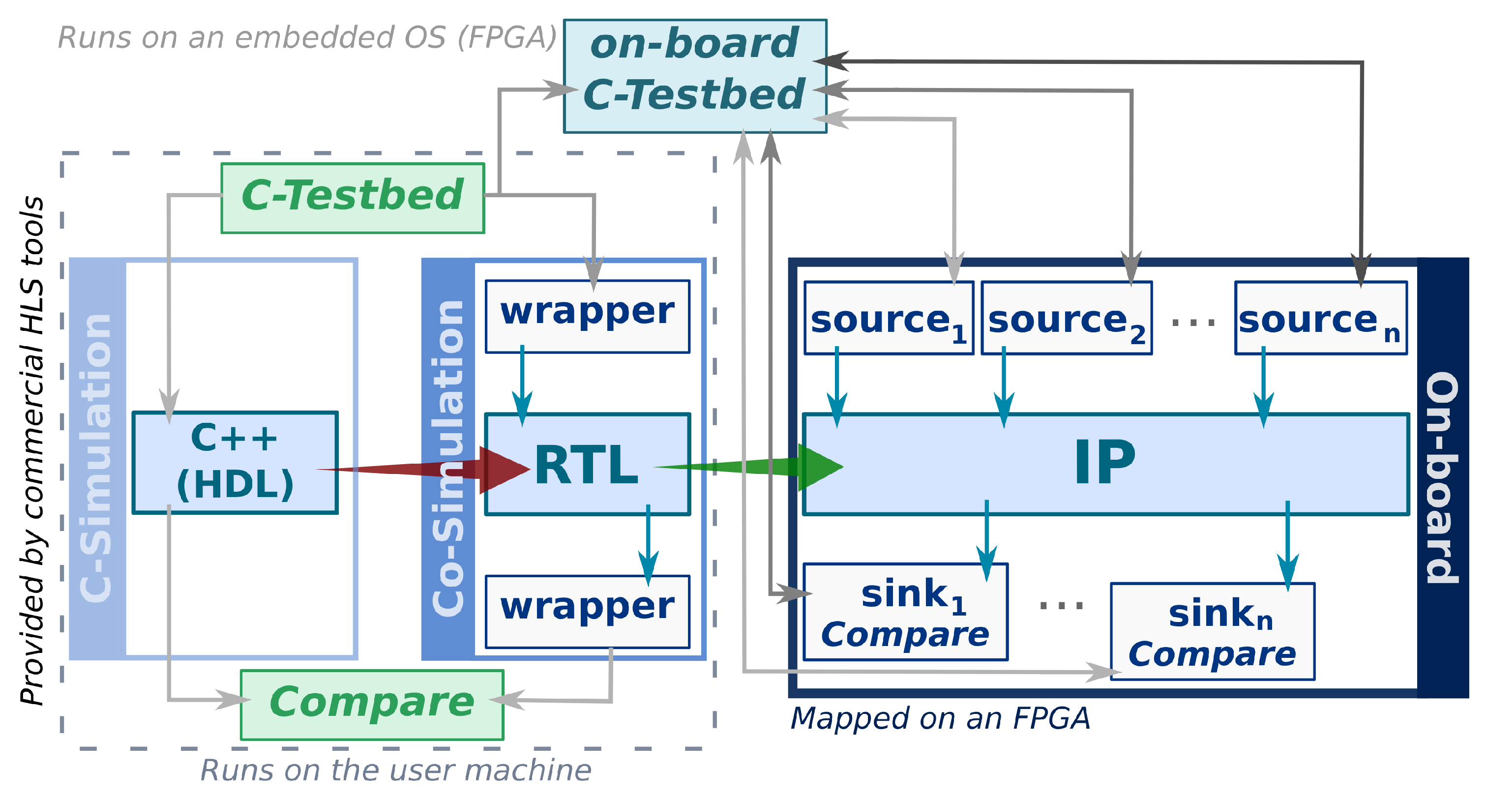
Unfortunately, commercial HLS tools only cover the first two phases of pre-silicon activities (see dotted box in
Figure 1). On the one hand, commercial tools such as Vivado HLS from Xilinx or Catapult HLS from Mentor use the cosimulation and smoke testing strategies respectively to perform an RTL verification by instrumenting the testbench with wrappers that do not add additional code to the generated logic model. On the other hand, academic HLS tools, such as LegUp, provide some facilities to debug the HWacc in-situ but instrumenting the C code [
3], which adds new paths in the generated RTL and, hence, modifies the component under test.
In this article, a novel solution to mitigate the impact of the verification processes in modern FPGA-SoC design is introduced, but without altering the structure nor the component behaviour. This proposal combines techniques that are familiar to software engineers (unit testing) and seamlessly integrates in current design workflows supported by commercial HLS tools (see
Figure 1). According to [
1] verification activities account for, roughly, 60% of the development cycle, and it is exacerbated by industrial verification trends [
4]. In this sense, the focus of this work is on providing a solution to reduce the gap between pre-silicon and post-silicon verification activities when it comes to the use of HLS tools. This proposal is based on a set of tools and an on-board verification infrastructure for HLS-based modules. This paper has four main contributions:
A framework that automatically verifies a HWacc across abstraction levels, starting from their high-level description by using Docker images.
An automatic translation of the test cases from a timeless model to a timed one that allows designers to assess the timing development of a HWacc.
A set of timing and checking pragma directives that modify and verify the signal protocol, respectively. Such artifacts bring the facilities to explore an enriched set of testing scenarios that HLS tools cannot carry out.
A demonstration and a statistical comparison of the proposed hardware verification framework.
This paper is organized as follows.
Section 2 describes the related work. In
Section 3, we present the hardware verification framework that instruments HWacc for validation purposes, in which an FPGA-based platform is used to carry out such a process through Docker containers. In addition, we explain how the HWacc is verified across the abstraction levels by using the same testbed.
Section 4 presents an analysis of our hardware verification framework and compares the proposal presented in this paper with others. Finally,
Section 5 summarizes the major outcomes of our proposal.
3. Materials and Methods
Achieving high productivity in verification processes is desirable for design teams. In this regard, designers must use C-based executable models to decrease simulation times, whilst the rest of the design flow must be automated. Thus, designers could spend more time designing value-added solutions instead of building verification systems/platforms that are only valid for testing purposes and usually little or no reusable. When it comes to HLS-based design, designers only deal with a specification of the HWacc in a High-Level Language (HLL), such as C or C++, which is tuned and optimized until the design meets the requirements. To this end, designers must describe test cases to validate the HWacc and, then, analyse the reports produced by the HLS tool to decide the optimizations that will be applied in the next iteration. On top of this, the nature of HLS follows a timeless model because of the use of programming languages that do not include timing features. In this sense, tests are coded with the same programming languages and, thus, they do not allow to change the signal timing or interface protocol. These characteristics are desirable since they allow to stress the HWacc and cover more scenarios.
This work is featured by the use of testing frameworks, such as Unity [
13], to facilitate the description of the test cases and keep up a robust test structure [
14], whilst signal timing requirements are expressed as pragma directives. The rest of the verification tasks, co-simulation and on-board verification stages, are automated by our hardware verification framework, which is able to interpret the timing requirements that have been included by the designer into the test cases. For example, our framework is able to check the temporary behavior of the HWacc that C-Simulation and Co-Simulation steps cannot, because of the nature of their timeless model. Thus, this proposal follows the principles of high-level productivity design, which drives the designer’s effort towards designing the ideal solution.
Following the design flow of the HLS-based high productivity design methodology, that has been extended by our hardware verification framework, the first transition (red arrow in
Figure 1) translates the C specification into the RTL code. The RTL model is instrumented by the HLS tools with a set of wrappers for verification purposes. Stimuli are extracted from the execution of the software simulations and stored for later use in the Co-Simulation and on-board verification stages. The second transition (green arrow in
Figure 1) creates the bitstream from the RTL generated in the previous stage. At this point, the HWacc is automatically instrumented with hardware components, source and sink, that replace the wrappers of the Co-Simulation stage to exercise and compare the results of the HWacc, respectively. The source components exercise the HWacc under test, whilst the sink components compare the results obtained with the expected values. Previously, the test cases written to verify the correctness of the C/C++ model are automatically adapted by our verification framework, so they can be reused during on-board testing without any extra work required from the designer.
3.1. On-Board Verification Environment
The proposed on-board verification environment is based on FPGA-based hybrid platforms, whose architecture is divided into two parts: the Processing System (PS) where test cases are executed; and the Programmable Logic (PL) where the HWacc is instrumented with source and sink components. A fourth component is responsible for orchestrating the verification process in the PL part.
3.1.1. Instrumenting the HWacc
To make the testing process transparent to the software and, at the same time, independent of the hardware platform, the HWacc interfaces with the infrastructure through source and sink components. These components provide or consume data to/from the HWacc, respectively, as
Figure 1 shows. In this sense, we consider the source components to be the initiators because they feed the HWacc by writing values into data input port, whilst the sink components are the targets because they ingest data from an output port of the HWacc. In the current version of the verification platform, only AXI-Stream interfaces to the HWacc are supported, since it is the interface most commonly used [
15,
16] in this type of accelerators. Even though other types of interfaces or protocols are out of the scope of this work, but they could be adopted following a similar approach. Each AXI-Stream interface of the HWacc is connected either to a source or sink component, i.e., the hardware verification platform must provide as many of these components as the HWacc needs.
Source Instrumenting-Component
The source exercises the HWacc through an AXI-Stream packet emulating the behavior of the actual producer component in the final system. The stimuli and timing/signal attributes associated to a source are read from a pre-assigned memory space in DDR memory and, then, stored in the internal buffer of the source component. Thus, the source is inherently capable of buffering data and understands the behavior of not mandatory signals, such as TLAST signal of AXI-Stream protocol, and the time in which the signal must be set/cleared. Each TDATA value is associated to a last and a delay values; the former marks the boundary of a packet (TLAST signal), while the latter establishes the number of cycles that the TVALID signal must be low before set it (delay). In brief, source components can generate AXI-Stream packets with delays, something that cannot be done by HLS tools because of their timeless model, i.e., only ideal testing scenarios are feasible with HLS tools, where there are no data delays or protocol handshaking is always fulfilled. In consequence, through our verification platform, designers can explore an enriched set of testing scenarios where the HWacc is exercised to check for protocol correctness at cycle level through timing pragma directives included in the test cases. Again, HLS tools cannot handle these scenarios and, therefore, are not able to ensure that the HWacc would work correctly under no ideal scenarios. Our verification framework is able to understand such pragmas embedded in the test cases, which, in turn, are translated from a timeless model to a timed one by adding delays (if they are specified) between stimuli. Thus, developers can observe and analyze the adverse effects of delays in the HWacc under test. The timing pragma directives that alter the timing behavior of the AXI-Stream signal set, except for the TDATA signal, are the following:
rand: Generates random values.
none: No signal check. Ideal packet is generated.
<file>: Binds the signal values to the contents of a file.
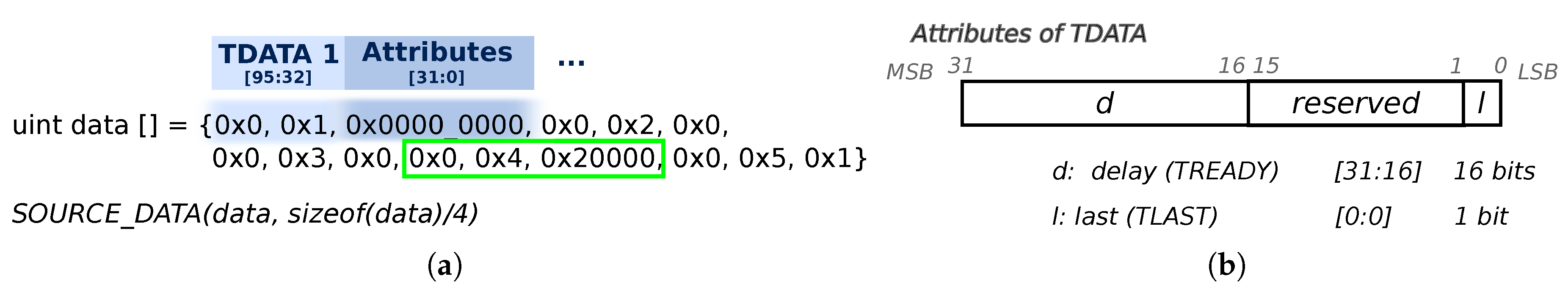
From a technical point of view, data is organized in
N-bit + 32-bit packets, where
N is the width of the
TDATA signal (expanded to multiples of 32-bit words) and the following 32-bits encode the attributes of such
TDATA (delay, last, ...). These packets are stored in the off-chip memory without padding (no gap) between them, so it is minimized the waste of space due to internal fragmentation when the word size of
TDATA differs from 32 bits. For the sake of simplicity and ease of debugging of the prototype at signal level, this parameter is fixed to 32 bits (see
Figure 2b): (1) 16 bits to specify the delay (
TREADY) and; (2) the other 16-bits are devoted to code current (e.g.,
TLAST) and future attributes that could be added (i.e.,
TKEEP). These sizes can be adjusted, reducing the overhead due to side-channel information requirements.
In the end, the source component must deserialize the data it receives from the DDR. The logic in charge of the interpretation of the byte stream is implemented by an FSM (Finite State Machine). This FSM separates the different parts (
TDATA and its attributes) of a stimuli packet.
Figure 2a represents the software function that copies in source’s memory address space the stimuli corresponding to five samples. The values of vector
data[] are automatically generated by our verification framework out of the trace of the C-simulation and with the help of the timing pragma directives.
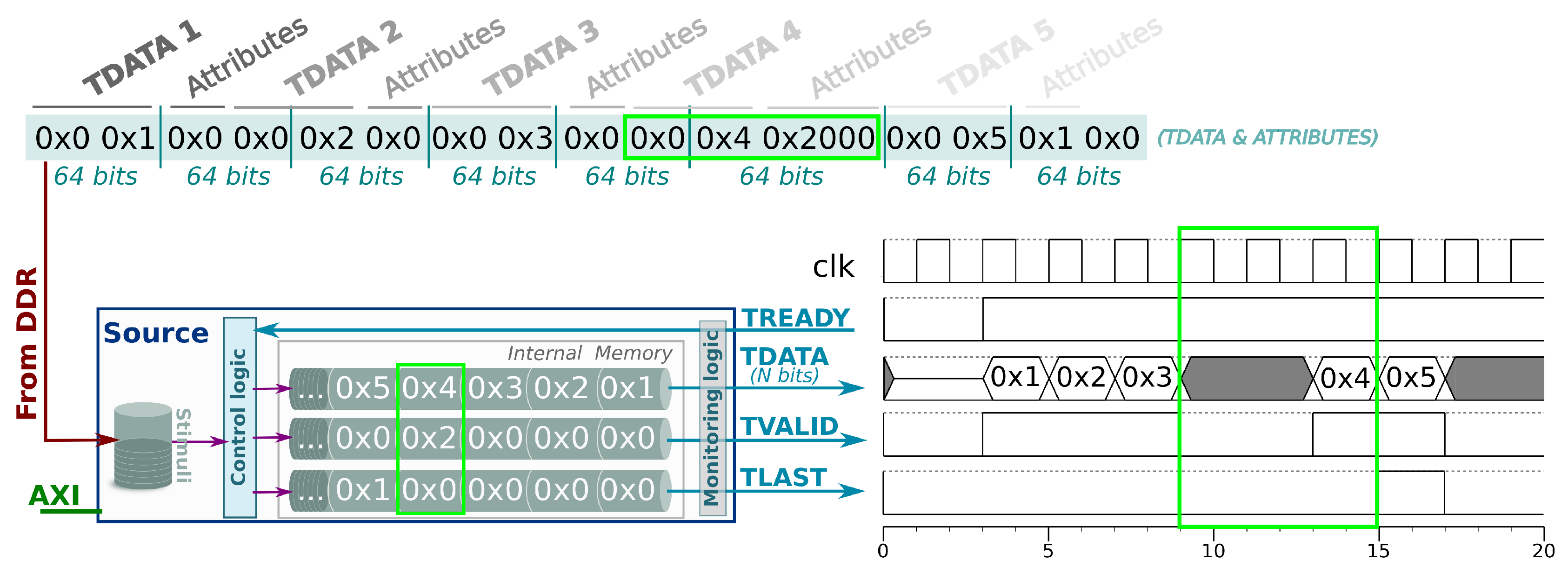
Figure 3 depicts the layout in the off-chip memory of the same five stimuli samples, after the execution of the
SOURCE_DATA function. Then, the memory data are read by the source component, temporarily stored in the local FIFOs and finally resulting in a specific sequence of signals to exercise the DUT. In this example, one sample has been bounded with a green rectangle, so the reader can easily trace it through
Figure 2a and
Figure 3.
As it can be seen, despite the fact
TDATA size is 64-bit, the alignment of the
TDATA samples do not have to be forced to 64-bit, no padding is added and, therefore, no useless bytes are left in memory. Furthermore, the width of the input AXI Memory interface in the source component, through which the stimuli are received, may vary depending on the platform on which the on-board testing infrastructure will be implemented. The control logic module is the main responsible for interpreting the streaming of stimuli and store them in the corresponding FIFOs. This fact makes it possible to separate the data memory access from the testing issues, but achieving a high bandwidth. Thus, using one target platform or another does not imply a change in the testing model, but it requires a change in how data are transferred from off-chip memory (see
Section 3.1.4).
Concerning the time diagram, the delay value of the first sample must be 0, that is, the AXI-Stream signals are assigned to their corresponding values when the handshaking enables it (
TREADY is set). The boundary of a packet can be marked by the value
0x0001 in the last attribute of the last sample, however, designers can indicate as many of last indicators as they need, to set the
TLAST signal at will.
Figure 3 also illustrates an AXI-Stream transfer with delays, in which the fourth value is delayed 2 cycles (highlighted in green).
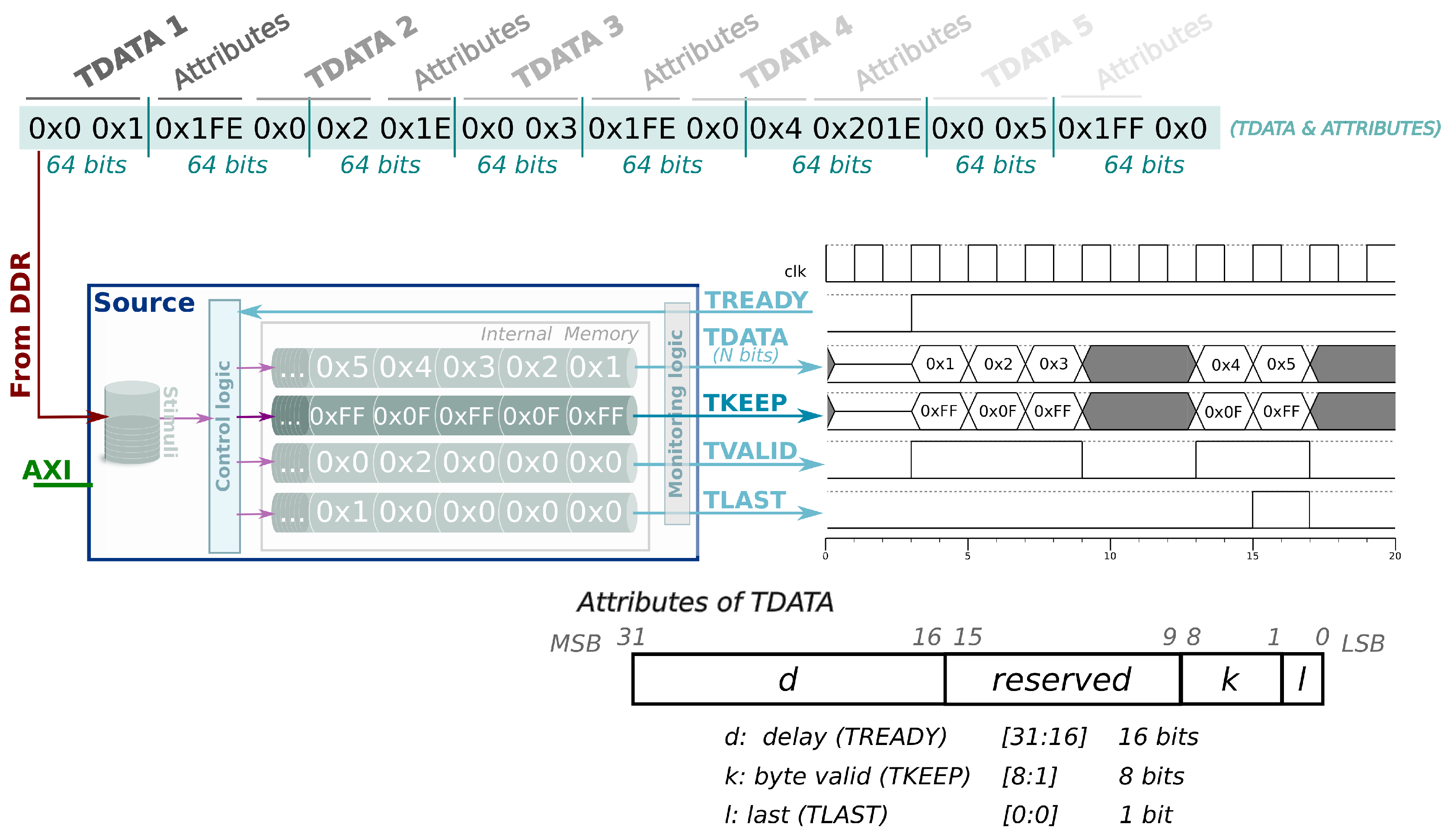
Although the signal set of AXI-Stream protocol has been limited to the
TREADY, TDATA, TVALID and
TLAST signals, the rest of them, such as
TKEEP, could be included following the same approach. In the example shown in
Figure 2b, the 32-bit word, in which the attributes are encoded, contains some unused bits, so the
TKEEP can be managed as a new attribute (see
Figure 4). To this end, the control logic module must be modified to interpret this new attribute, the rest of the modules of the component work as they have been doing.
Sink Instrumenting-Component
The sink components compare at run-time the output of the HWacc with the expected values and, also, check the clock cycle in which the output is generated. Thus, our verification framework moves part of the comparison process from test cases to the sink components. To do so, the reference output values are stored in the sink component according to the two following rules.
The delay value indicates the maximum number of cycles between the current TDATA and the previous one, i.e., the time window in cycles in which the TVALID signal could be set. When the delay is 0xFFFF, it means that TDATA can be received at any time, and it is not checked.
The rest of attributes contain an extra bit that depicts if such attribute must be checked. For example, the TLAST signal has two bits, one to specify the expected value and the other to point out the action that must be performed. A value of 0 in this second bit means that the attribute must be checked, whilst 1 indicates that the attribute is not considered during the test process.
Like source components, sink components read the reference output vectors and the attributes associated to each data value from external memory (DDR). The sink components also store a trace of failure when the HWacc output mismatches the expected one. Such trace contains an error flag to identify the source of the error: 001 for TDATA error; 010 for TLAST error; 100 for TVALID error. The sink components are also capable of detecting multiple failures in the same sample by an OR operation. For example, 011 means that TLAST and TVALID were wrong.
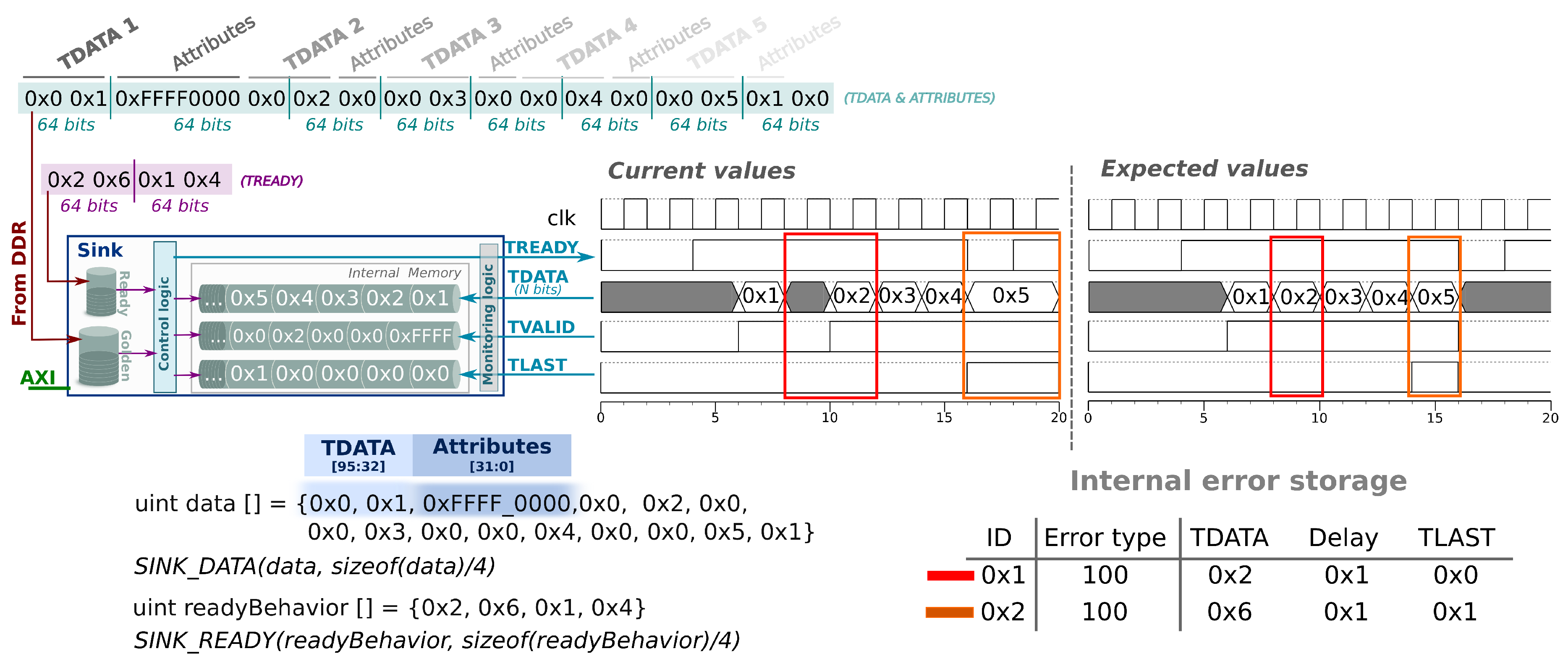
Figure 5 illustrates an example of the sink component with two timing diagrams: current values on the left (AXI-Stream packet with delays caused by the HWacc and by the
TREADY signal) and expected values on the right (AXI-Stream packet without delays). HLS tools would consider both diagrams correct, since co-simulation technology is not able to detect delays or violations of the protocol. By using the proposed verification framework, the designer is able to check the value of
TVALID signal and control the
TREADY signal to force specific scenarios and look for wrong behaviours of the HWacc. From a technical point of view, the delay attribute of the first expected sample must be assigned to the reserved value
0XFFFF for synchronization purposes. The first sample is the beginning of a transfer and the sink component does not have a reference signal-time arrival from a previous sample. Also, the first sample (
0x1) is correct because the value of the data is the expected one and the
TLAST flag is not set. In this case the delay is not taken into account because it is the first data. However, the second sample (
0x2) arrives one cycle later than expected, so the sink component notifies this failure by denoting the error type found (highlighted in red). The sink component keeps looking for mismatches and, in the actual example, another failure takes place in the last sample. The expected delay must be one, but the current delay is two because the
TREADY signal is not set during one cycle (highlighted in orange). The third and fourth samples (
0x3 and
0x4) are not failures because the arrival time is correct; we take as the reference the arrival time of the previous samples.
In addition, the sink component handles the
TREADY signal to disable the output of the HWacc in order to force borderline scenarios. For example, the internal storage (such as FIFOs and BRAMs) of the HWacc can collapse and, depending on the implementation, the HWacc could either discard values, which may lead to
TDATA and
TLAST errors, or block the HWacc, which produces
TVALID errors. It is worth mentioning that such kind of use cases are impossible to be emulated with the testing facilities provided by current HLS tools.
Figure 5 also shows how the sink component handles the
TREADY signal as it is specified in the
readyBehavior array. Starting with 0, each element in the array represents the number of clock cycles the value of
TREADY is maintained before complementing it. In this example, after two cycles, it is set during six cycles and then it is cleared for one cycle, causing a failure in the last sample (highlighted in orange).
Furthermore, both components, source and sink, provide more information, such as the number of samples consumed and produced by the HWacc, respectively, and the rate at which the data is consumed and produced. Thus, designers can determine if the speed rate achieved is enough to validate the HWacc or it must be optimized.
3.1.2. Mapping the HWacc
The source and sink components isolate the HWacc from the rest of the platform. This configuration allows to apply partial reconfiguration techniques to significantly speed up the synthesis process of the whole design. Thus, the on-board verification platform defines a Reconfigurable Partition (RP) where varios HWacc can be mapped as Reconfigurable Modules (RM) by using the Dynamic Partial Reconfiguration (DPR) feature present in some FPGAs architectures [
17]. In this sense, pre-built parts (checkpoints) of a previous project, which have been synthesized, are reused to reduce the synthesis time of a new HWacc in order to make the FPGA iteration faster. In the case that a HWacc does not fit in the RP, because there are not enough FPGA resources to allocate its logic, the DPR feature is not valid. In any case, the process to generate the configuration file (partial and full bitstreams) is completely automated by our verification framework by means of TCL scripts.
3.1.3. Orchestrating the Verification Process
All components are connected to an orchestrator component, whose objective is to oversee the verification process in the PL part, following the implementation shown in [
18,
19]. The orchestrator can be controlled, in turn, by the software part of the test case, which runs on the PS part. The designer of the test cases can make it use of some high-level test functions provided as a library:
The RCUNITY_RESET resets all components in order to assure that the verification environment starts from a well-known state.
The RCUNITY_START(c) enables the HWacc during c cycles and then halts the system, but the information stored in the source and sink components can be accessed by the test cases. The HELD_HIGH value is reserved to permanently activate the HWacc.
3.1.4. Hardware Verification Environment
In this section, we describe the big picture of the hardware verification platform and an overview of the test flow on the hardware side. The software side is detailed in
Section 3.2, where it is explained the extension made on a well-known software testing framework so it can be play the role of test manager in the proposed on-board verification infrastructure.
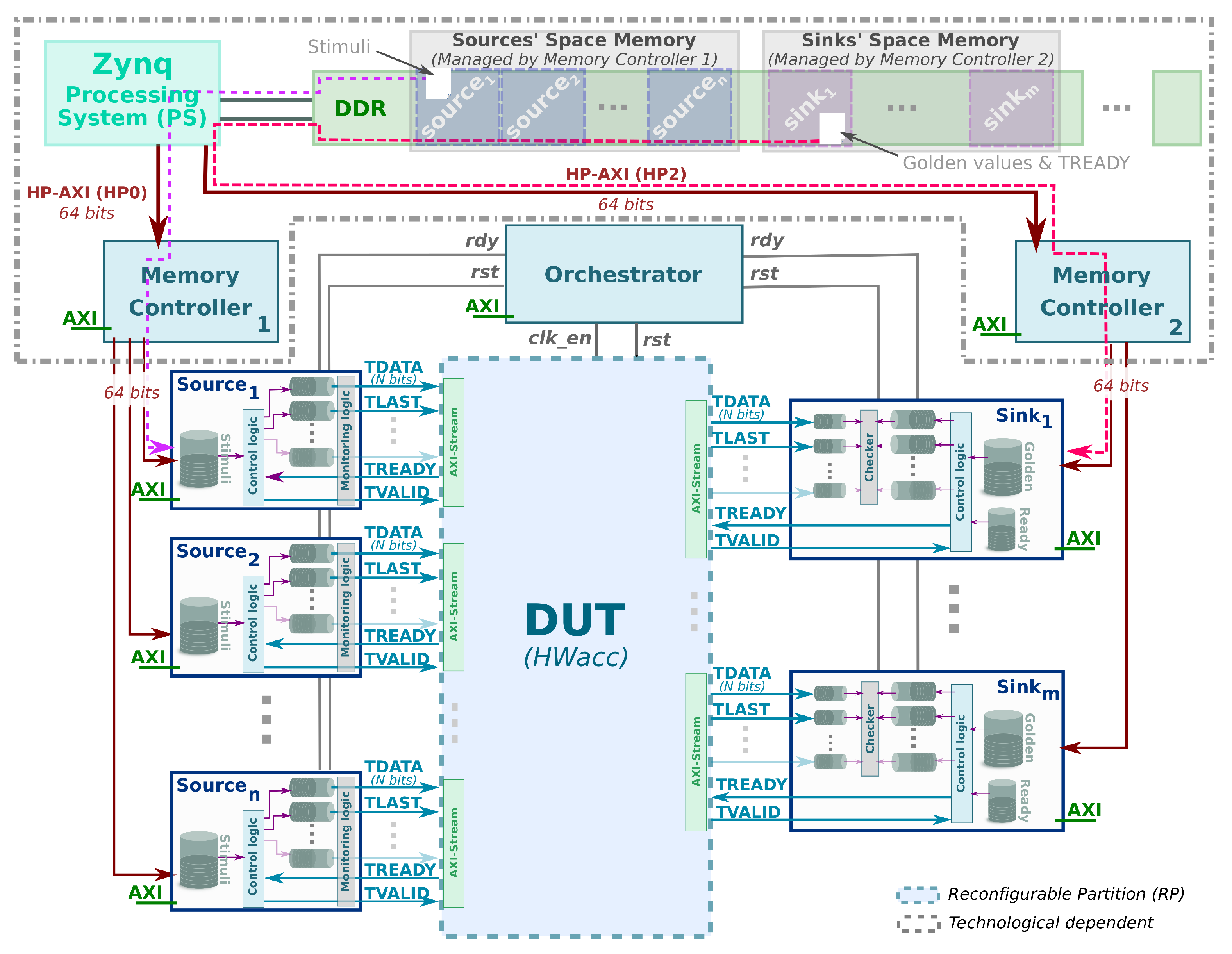
Figure 6 shows an overview of the architecture layout of the hardware verification platform presented in this manuscript. Such architecture contains an RP (Reconfigurable Partition) in which the HWacc is placed during the place & route stage (see
Section 3.1.2). In addition, there are several hardware components around it that allow to proceed with the verification process as follows.
Firstly, the HWacc (DUT) must be developed using HLS and verified at RTL level by using the facilities provided by the HLS tool. During this step, the functional simulation (timeless) of the C or C++ model takes place, producing a set of intermediate files with the trace of the inputs and outputs. Thus, our hardware verification framework is able to automatically extract the stimuli and the golden values from the files generated by the HLS tool. Besides, the timing annotations, which were included in the test cases through the timing pragma directives, are processed and combined with the values extracted from the timeless model. The result is stored in different regions of the off-chip memory (DDR) in which has been divided and assigned to each source and sink component at design time.
Then, the memory controller components read from the DDR the stimuli and golden values as they are needed. That is, the movement of data from DDR memory is made on demand. Since each source and sink component is independent of each other, they are able to issue read requests to the memory controller independently. The memory controller will be responsible for dynamically scheduling the access to the DDR, trying to minimize the waiting times and maximize bandwidth. To help in this goal, each source and sink component is configured with a threshold value that is used to trigger a new request to the memory controller. If the internal buffer empties below such threshold, the source or sink asks for a new block of data to the memory controller (see pink and red dotted arrows in
Figure 6).
It is worth noticing that each source/sink may have a different read pattern of the stimuli/golden data samples. This is highly dependent on the specific application and traffic pattern. Therefore, it is the designer who sets a collection of architectural parameters for such infrastructure at design time so as to get the best tradeoff between the use of resources and the total bandwidth achieved (e.g., size of the internal memory buffers, size of the read request to memory or value of the threshold, etc.). The designer is free to make the best decision based on the aforementioned memory traffic characteristics for each channel. So, for example, one memory controller can be the hub for five components whilst another can handle just two. Everything depends on the estimated aggregated memory traffic that is expected to be generated by the set of sink or source components that connect to a single memory controller.
The execution of the test will start as soon as the source and sink components have enough data to operate. To this purpose, the orchestrator component freezes the HWacc (i.e. disables the DUT clock) and waits until these components are ready to start. Previously, the orchestrator must be configured as is explained in
Section 3.1.3.
Once the hardware verification stage has been finished, the test case retrieves information from the source and sink components concerning metrics about the execution of the test such as the speed rate of each AXI-Stream interface or the number of samples exchanged through such interface. For the sink components, the test case can enquiry about the number of errors or mismatches (see
Section 3.2). Thus, developers can dispense the use of timing diagrams for analysis purposes, which results in highers levels of productivity.
It must be mentioned that although
Figure 6 shows an overview of our hardware verification platform, implemented on a Zynq-7000 FPGA-SoC (Digilent Inc., Pullman, WA, USA), the proposed solution abstracts the verification process from the final target platform. One of the major concerns is the facilities offered by the selected platform to access external memory (where the stimuli will be stored), which may differ in efficiency, services, architecture, etc. In order to overcome this technological challenge, the hardware verification platform isolates the source and sink component from the specificities of the target platform. Thus, the memory controllers are the components that depend on the technology used and are custom implemented to achieve the highest possible performance (see grey dotted box in
Figure 6). In this platform, the internal memory of the source components is filled by a memory controller, whilst the internal memory of the sink components is flushed to DDR by another memory controller. From a technical point of view, the memory controllers, implemented on a Zynq-7000 FPGA-SoC, are connected to the off-chip memory through the PS using different HP-AXI buses, HP0 and HP2, that allows them to work in parallel. This fact is possible because there are two physical buses that connect the off-chip memory with the SoC, whilst the Zynq-7000 FPGA-SoC organize them into two pairs of logical buses, i.e., HP0 and HP1 use one physical bus, whereas HP2 and HP3 use the other one. In addition, each memory controller is connected to the PS through two independent AXI-Interconnect components in order to remove the bus arbitration (not depicted in
Figure 6). Thus, memory controllers are able to perform several burst transfers of 16 64-bit words to fill, as fast as technology allows, the internal memories of the hardware instrumenting components.
Internally, one memory controller instantiates an AXI Data Mover IP [
20] from Xilinx, which could be regarded as the component that implements the core logic of a DMA engine. The AXI Data Mover receives commands through a FIFO-style port that trigger memory transfers. The logic surrounding the AXI Data Mover IP instance is responsible for issuing commands to the AXI Data Mover anytime the data is needed (source) or ready to be written in memory (sink).
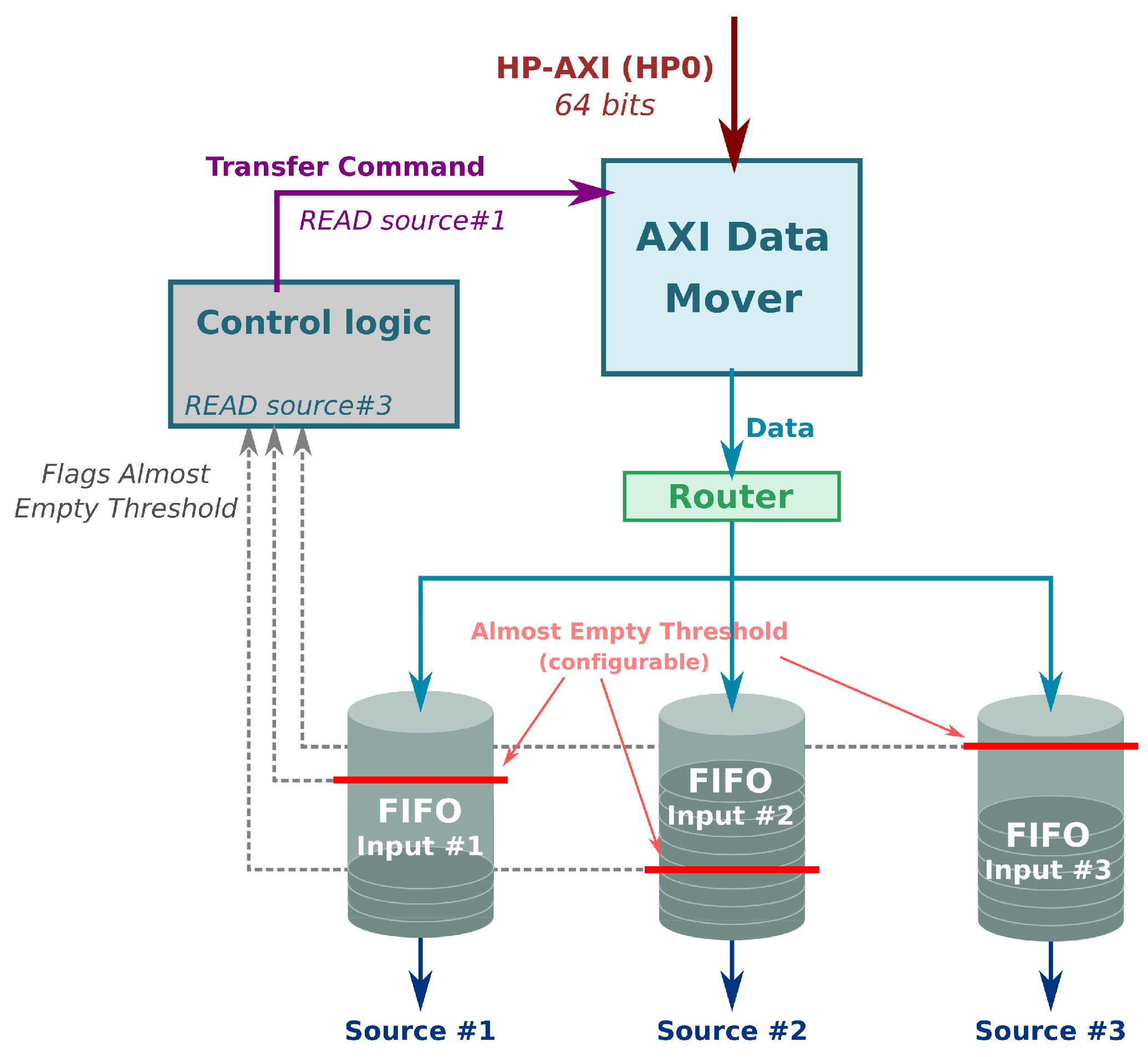
Figure 7 sketches the block diagram of the memory controller for the Zynq architecture. In the represented use case, three source components are connected to the same memory controller. Each source component has its own FIFO, whose data is being consumed by the DUT. If the amount of data falls below a specific level (configurable for each one), the control logic issues a read command to the data mover. In addition, the control logic plays the role of arbiter whenever two or more FIFOs run out of data at the same time or while there is a pending memory transfer. On top of a configurable definition of the FIFO almost empty thresholds that triggers new read commands, it is also possible to adjust at run time parameters of the memory transfers such as the length of a single data beat or the total length of the burst. This is crucial to minimize the dead cycles when transferring the data between memory and the source components and depends on the specific traffic patterns for each source or sink.
Regardless of the specific technology used to implement the memory controller, it is worth noticing that this component is key in pursuing the goal of keeping the testing infrastructure independent of the target platform. Thus, the main benefit is that sources and sinks are independent of the memory interface used and its parameters (data width, access protocol, etc.).
For example, the EK-U1-ZCU104-G (Zynq UltraScale+) board provides completely different hardware facilities as to the access to external memory compared to the ZedBoard (Zynq-7000 SoC). This fact allows us to define a new strategy, while maintaining the same architecture, based on the use of the memory controller. In this new scenario, the best option is based on the use of a single memory controller that provides access to the off-chip DDR memory. All source and sink components of the DUT are connected to this version of the memory controller. The main difference is the protocol access to the DDR, through the user interface protocol of a MIG (Memory Interface Generator) IP [
21]. In this sense, the MIG IP replaces the AXI Data Mover for the ZCU104 board and thus the controller must be modified. However, the rest of the testing infrastructure is isolated from this change, making it easier and fast to move from one prototyping platform to another.
3.1.5. Distribution through Docker Images
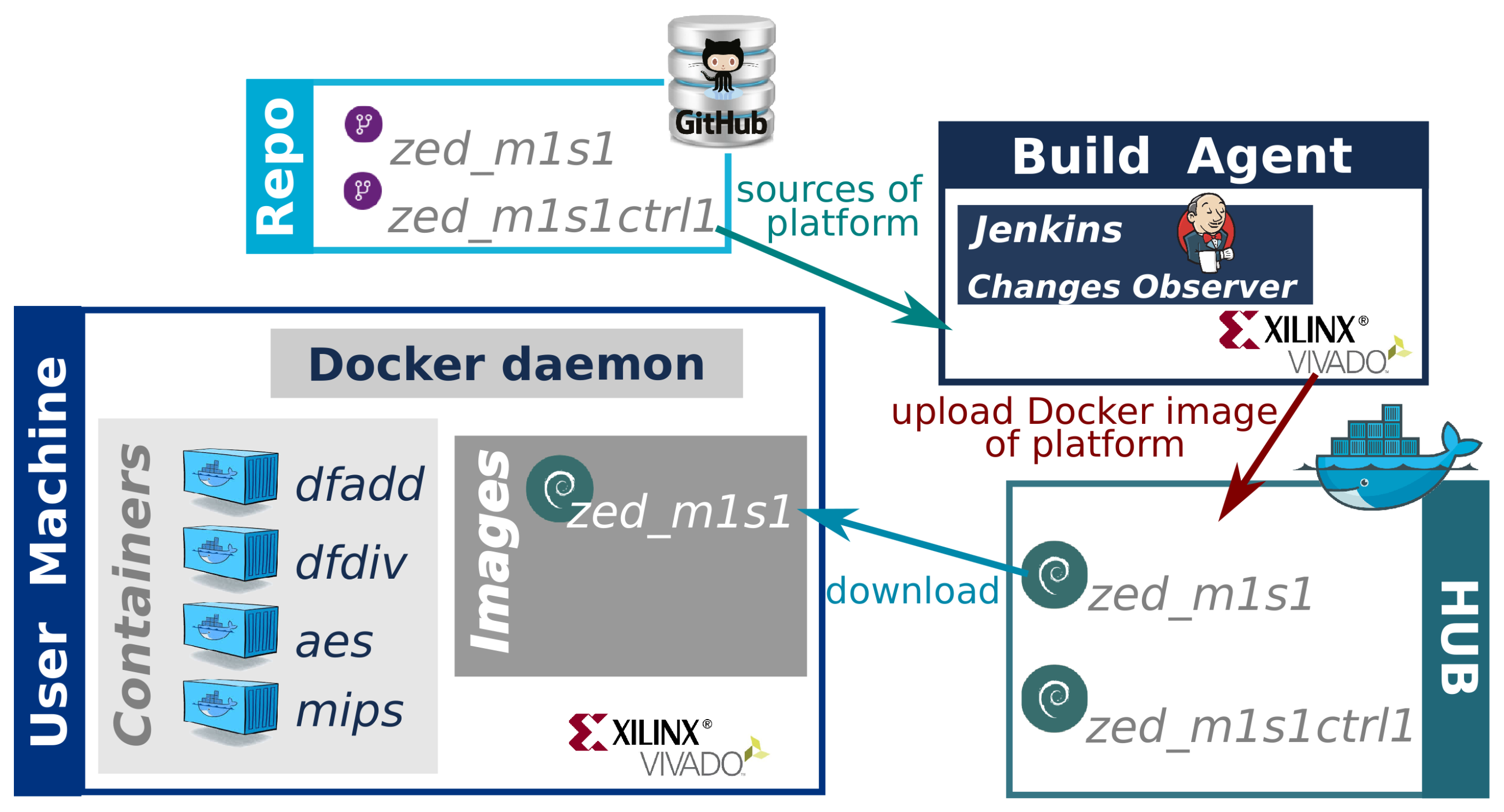
In order to facilitate the distribution of our hardware verification framework, a set of Docker images have been built. The set of images are warehoused in what is called a Docker Hub. The use of Docker technology greatly facilitates the work of the final users of our hardware verification platform. The final user only has to download a Docker image from the Docker Hub to their computers and create a container (see
Figure 8) where they can launch the HWacc verification process. A Docker container packages up libraries, tools, environment variables, code, etc. of our framework and all its dependencies so the verification runs quickly and reliably from one computing environment to another. In this regard, it is considered a lightweight, standalone, package of software that provides an isolated and clean environment to test the HWacc.
Docker images can be built and released by anyone. The process to create a new Docker image is automated. To this end, the developer of an image must link a GitHub repository, which contains the source code of our hardware verification platform, with a Jenkins Agent (Build Agent in
Figure 8). This agent is the main responsible for building the Docker image by synthesizing the static components of the hardware verification platform that will be deployed in the on-board verification stage. Thus, the user of the image is freed from the time consuming task of generating the bitstream for the whole design, only needing to synthesize the DUT that will be deployed in the Reconfigurable Partition (see
Figure 6 and
Section 4). Finally, the Build Agent automatically uploads the Docker image to the Docker Hub.
3.2. Test Cases across Abstraction Levels
In this section, it is shown how our proposal allows verification activities across abstraction levels, using as the driving use-case the implementation of a HWacc for the
dfadd CHStone benchmark kernel on a Xilinx ZedBoard FPGA. Following the design flow, designers must start with the description of the test cases to verify the high-level model of the HWacc. Thus,
Listing 1 shows one of the forty test cases written for the
dfadd kernel, which performs a sum operation of two 64-bit words and return the result into another 64-bit word. This test case includes two timing pragma directives that randomly alter the timing behavior of the
TVALID signal of the source component and the
TREADY signal of the sink component (lines 2 and 3 of
Listing 1, respectively).
Apart from the set of timing pragma directives that modifies the timing behaviour of the AXI-Stream signals, there are three checking pragma directives that allow designers to verify the requirements of HWacc that are not feasible in C-Simulation because its timeless model or are not automated in Co-Simulation in which designers must manually analyze the generated timing diagram.
delay: Check that the delay of the HWacc is within a range of cycles, which is depicted by the variables max and min, whose aim is to denote the maximum and minimum number of cycles to complete the operation, respectively.
inputs: Check the number of input values that the HWacc has consumed. The designer must depict the number of inputs as a range through the variables max and min.
outputs: Check the number of output values that the HWacc has produced. The designer must depict the number of outputs as a range through the variables max and min.
By default the
min variable of all checking pragma directives is 1. The test case listed in
Listing 1 includes a checking pragma (line 3 of
Listing 1) that restrict the time to complete the operation of the
dfadd kernel, it must be completed 32 cycles, i.e., the test case will check that the
adder64 function is done within 1 and 32 cycles, thus if the time completion is greater, the test will fail.
Listing 1. Test case for dfadd kernel.
Once the writing of the test cases is complete, our framework automatically generates the test runner, a function that orchestrates the execution of all of them in the software side, following the guidelines of Unity testing framework [
13]. Then, the source files are compiled and executed to validate the behaviour of the C code (C-Simulation). In order to validate the RTL model, the HWacc HLS model is synthesized and Co-Simulated, using the same test runner and testbed.
Listing 2 shows the Co-Simulation report after execute the same test cases that were executed in C-Simulation; the C-Simulation report is omitted because it is similar to the Co-Simulation one.
Then, in order to perform the on-board verification, our framework launches the synthesis process to obtain the bitstream and adapts the test cases to the new environment.
Listing 3 shows how the test case generated from the one in
Listing 1 looks like. No new code is needed to be written by the designer, and the stimuli are taken from the test cases.
Listing 2. Co-Simulation report of dfadd kernel.
...
// RTL Simulation : 39 / 40 [75.00%] @ "5055000"
// RTL Simulation : 40 / 40 [100.00%] @ "5255000"
...
ut_dfadd.cc:437:test_a_n1_b_0_z_n1:PASS
ut_dfadd.cc:444:test_a_n2_b_1p5_z_n0p5:PASS
---------------------------
40 Tests 0 Failures 0 Ignored
OK
Nonetheless, the designer can get control over some features of the test process by using different timing pragma directives (e.g., lines 2 and 3 of
Listing 1). The first one sets a random delay between stimuli, thus the second
TVALID signal is set 16 cycles after the first one because the value
0x00010010 (lines 4 and 5 of
Listing 3) indicates that the second value is the last one (
0x0001) and it must be set after
0x0010 clock cycles. It must be mentioned the stimuli is composed by two 64-bit words, which are represented as four 32-bit words in the
data_in_1 array of
Listing 3, followed by the timing notations, delay and last attributes. Meanwhile, the latter timing pragma directive establishes a random behavior of
TREADY signal (line 3 of
Listing 3); it will be set low the first 5 clock cycles, high during 2 cycles, low the next 10 cycles and so on. In addition, the same pragma also selects the signals to be checked and its mode, in this case neither the
TLAST signal nor the
TVALID signal are checked because the reserved value
0xFFFF is present in the golden vector (lines 6 and 7 of
Listing 3).
Listing 3. On-board test case.
Furthermore, the designer can add other testing features that are only feasible in the on-board verification by using checking pragma directives, e.g., line 4 of
Listing 1. This pragma is translated into an assertion that assesses that the time completion of the HWacc is less or equal than the specified in the
max variable (line 19 of
Listing 3). In addition, the
SINK_ASSERT_PASS higher-test function (line 21 of
Listing 3), which is automatically included in the test cases, assesses three rules; firstly, the number of failures is zero, secondly, the number of input and output samples is at least one, and thirdly, the delay is greater than one. If all are true, the test will pass. Thus, the default requirements imposed by the checking pragma directives are checked.
Later, newly test cases are compiled to get an executable file that runs on the embedded ARM processor in order to exercise the HWacc.
Listing 4 shows the report after execute them that displays the number of exchanged samples by the HWacc. In this case, the HWacc processes 2 words of 64-bit width and returns a words of 64-bit width, which are the return value of the
dfadd kernel. Alongside the exchanged samples, the report also displays the speed rate of transactions, which had taken place between instrumentation components (sources and sinks) and the HWacc, as well as the delay in cycles to complete the kernel operation.
Listing 4. On-board report of dfadd kernel
[SOURCE INFO] Exchanged Samples: 2
[SOURCE INFO] Digest Rate (words/cycle): 0.512639
[SINK INFO] Exchanged Samples: 1
[SINK INFO] Produce Rate (words/cycle): 0.285714
[SINK INFO] Not failures found
[INFO DELAY] 29
ut_filTest.c:1311:test_test_a_n1_b_0_z_n1:PASS
---------------------------
40 Tests 0 Failures 0 Ignored
OK
In order to show that our verification framework detects mismatches between golden values and output ones, the data of the golden output has been increased by one and the checking pragma directive related to the delay is reduced by 10 cycles (
#pragma FIL_CHK delay max=22); this change will produce a failure.
Listing 5 shows the stack of the new report that displays the trace of failure found by the sink component. Such trace, whose identifier is 0, shows that the error is located in the data because the value of the error type is
001. Meanwhile the time completion exceeds the requirement depicted via timing pragma directive, which is shown as a failure message. It is worth mentioning that the delay that shows the stack could be different that the one displayed by the line labeled as info delay; the first refers to the time in which the output data is ready and it is individual for each output value, whereas the second is the overall time to process the input values, i.e., from the reading of the first input to the writing of the last output.
Listing 5. On-board report of dfadd kernel (failure found).
[SOURCE INFO] Exchanged Samples: 2
[SOURCE INFO] Digest Rate (words/cycle): 0.512639
[SINK INFO] Exchanged Samples: 1
[SINK INFO] Produce Rate (words/cycle): 0.285714
[SINK INFO] 1 failures found
Showing stack!!!
[SINK INFO] ID: 0
[SINK INFO] Error type: 1
[SINK INFO] DATA: 0xbff0000000000001
[SINK INFO] DELAY: 0x1C
[SINK INFO] TLAST: 1
[INFO DELAY] 29
ut_filTest.c:1373:test_test_a_n1_b_0_z_n1:FAIL: Delay out of the range (29)
ut_filTest.c:1373:test_test_a_n1_b_0_z_n1:FAIL
---------------------------
40 Tests 1 Failures 0 Ignored
FAIL
4. Discussion
In this paper, we present a detailed description of our hardware verification framework that leverages the use of HLS tools for FPGA-based projects. As it was fully discussed in
Section 3, the proposed framework extends the features of HLS tools by including the on-board verification stage to complete the FPGA-based design flow. In this section, we would like to also provide a comprehensive analysis of the suitability of the proposed framework and compare it to other solutions.
The statistics in
Table 1 are gathered from the execution of test cases related to each kernel of the CHStone Benchmark [
22]. The test cases have been Co-Simulated in Vivado HLS and executed on a Xilinx ZedBoard, using our hardware verification framework. Both the minimum and maximum delay for each test case are shown. It is noteworthy the significant error detected in the times obtained for some of the CHStone kernels, which ranges from 5% to 66%. Focusing on the
dfsin kernel, which is the one with the highest relative error, the error increases with the number of test cases. It has been observed that the HLS tool builds a queue of stimuli, one entry per input to the HWacc. The latency of a single execution is measured starting from the time the stimuli for such test case is inserted in the queue. Therefore, this fact produces wrong timing profiling, leading the designer to wrong conclusions. Our solution measures the elapsed time just when the stimuli are read by the HWacc, and hence, it provides accurate timing results.
Furthermore, our verification framework obtains the number of samples consumed and generated by the HWacc under test. This information is relevant to determine the correctness of a design, because although the output will match with the reference values, the number of samples consumed could be wrong. Moreover, the verification framework also measures the rate of consumption and data generation by the HWacc.
Table 2 lists the rates obtained using two strategies: no delays (testing identical to Co-Simulation) and randomized delays in
TVALID and
TREADY signals, i.e., the handshaking of the AXI-Stream protocol is randomly modified to observe the behavior of the HWacc. It is worth mentioned the output rates are lower in the most kernels when delays are introduced. However, there are two particular cases (
jpeg and
sha) where the verification framework has not been able to obtain the rates because such kernels are blocked when the stream packets contain delays. The Verification IP from Xilinx [
23] allows this kind of packets through SystemVerilog but only in a Co-Simulation strategy. The time requirements is critical in some projects because they must meet hard timelines, i.e., the delays can alter the behavior of the HWacc or even result in wrong time responsiveness.
Unfortunately, the hardware instrumentation for debugging purposes entails a cost in terms of FPGA resources.
Table 3 shows the breakdown of resource usage of our solution (see last row), which has been divided into the two types of hardware instrumentation components: source and sink. Although other works use a different FPGA technology, as well as their experimental results were analyzed with other benchmark than ours, we have compared them focusing on the percentage of the hardware resources used, which are also listed in
Table 3.
It is worth mentioning that our hardware instrumentation components are the ones that need more resources because several reasons. On the one hand, our components contain all logic necessary to operate with the HWacc and with the PS side, whilst the works [
6,
24] do not include the storage resources in their analysis. These works follow the same strategy, internal signals are routed to the top of the HWacc under test in order to check them later, hence they must be stored on-chip memory or off-chip memory, but unfortunately that information is not provided. In the same line, J. Goeders and S.J.E. Wilton [
5] automatically route the internal signals to the on-chip memory, and then store the values of such signals when a store instruction is executed, i.e., a snapshot of the internal signals are stored several times to be analyzed by a software debugger later. However, this strategy entails an area overhead up to 25.4% over the original code [
5]. Moreover, these works provide an intrusive solution worsening the frequency of the HWacc, whereas our solution does not cause this effect. On the other hand, Y.H Choi et al. [
7] only displays the latency of each function, while K. Han et al. [
8] checks that their own protocol is correct in a Network on a Chip (NoC) by increasing a counter when the message is processed by one node of the network.
None of the works analysed provide an efficient way of generating stimuli like our approach does, i.e., our hardware verification framework is capable to model the signal timing behavior from a timeless model. Moreover most works do not check the behavior of the HWacc thorough a standard protocol, such as AXI-Stream. In this regard, the output interfaces of the HWacc can be blocked by the sink components setting the
TREADY signal, whilst the works [
5,
6,
24] depends on the depth of the memory in which the output values are stored. In addition, our framework bases the on-board verification stage on the use of pre-built parts of an FPGA-based project and the DPR feature, which makes a reduction of the synthesis time to obtain the (partial) bitstream.
Table 4 shows the synthesis time of each kernel. Unfortunately, a set of kernels does not meet the available hardware resources of the RP, but our approach is capable to synthesize the kernel without the DPR feature. Timing savings reach a factor of four in some kernels, and hence the FPGA-loop iteration is considerably reduced.
From the energy consumption point of view, the use of a Docker-based solution and pre-synthesized parts speeds up the (partial) bitstream generation as well as reduces the computing needs. This fact makes that the same host machine will be able to execute several Docker containers in parallel to obtain the corresponding bitstream files.
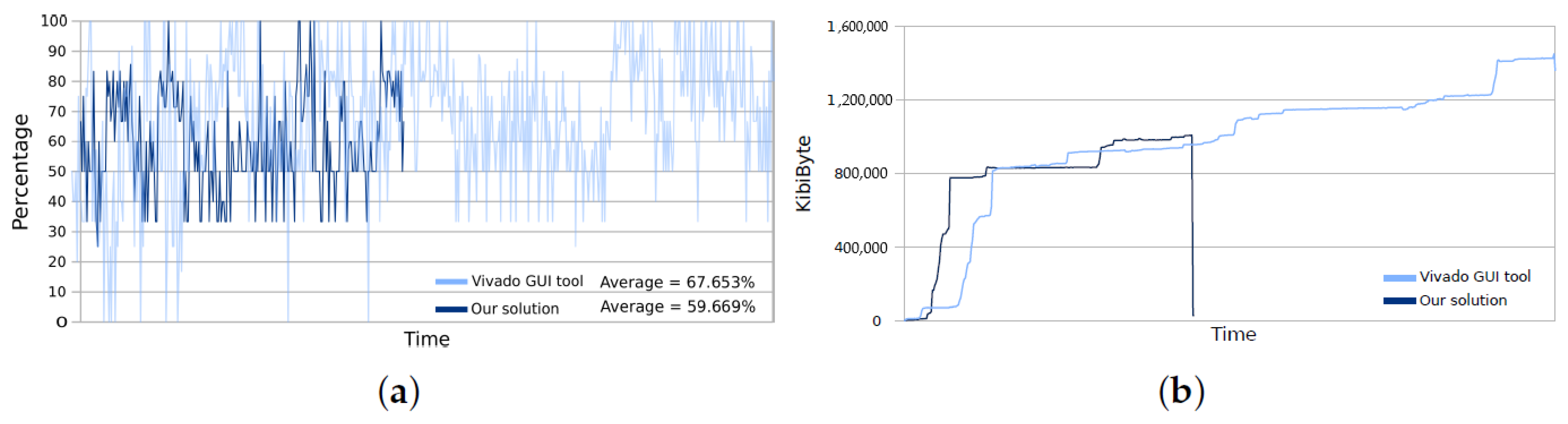
Figure 9 compares the consumption-power (
Figure 9a) and consumption-memory (
Figure 9b) between our approach and the Xilinx toolchain using its GUI mode for the
dfadd kernel. The CPU consumption-power is roughly 10% better when our approach is applied, besides our solution takes less time to perform a synthesis process than the GUI mode of Xilinx, so the CPU cores and memory are quickly released, around an average of 7 min per synthesis thanks to run the synthesis process in a Docker container in batch mode. The experiment had been synthesized in a GNU/Linux environment onto a CPU i7-3770 @ 3.4 GHz and 16 GB of RAM.
In addition to the computational benefits that Docker brings, it adds a well-maintained test environment avoiding the maintain difficulties, such as environment configurations, that provides value add to our hardware verification framework. Thus, engineers can, on their own development machine, spin up exactly the services and dependencies that would be available in production, but with their own hardware design deployed on top. In addition, engineers rarely have time to spend days or weeks “integrating” changes and testing them in a secure environment. Docker increases the productivity of development teams by allowing them to check the changes made in their designs through an automated and clean testing environment, which can be integrated with a Jenkins environment to reach continuous integration feature.


