1. Introduction
Recently, there has been extensive research developing sub-millimeter-wave and terahertz (THz) oscillator and power amplifier integrated circuits (ICs) using advanced transistor technologies [
1,
2,
3,
4]. Frequency multipliers are also widely used to generate THz frequency signals in ICs. They allow wide tuning range and low phase noise performance, compared to the fundamental oscillators at THz frequencies [
5]. Active
H-band (220 GHz–325 GHz) frequency multipliers have been reported in the form of IC using high-speed transistor technologies, such as GaAs metamorphic high electron mobility transistors (mHEMTs) or InP HEMTs and SiGe or InP heterojunction bipolar transistors (HBTs) [
6,
7,
8]. They can offer highly-integrated and low-cost THz signal sources, because they can be integrated with other circuits in the same semiconductor process [
7].
In
H-band, the low-order frequency multipliers, such as doublers, are usually designed to achieve high output power and high conversion gain [
6,
7]. The
H-band frequency doubler was designed in 90-nm SiGe HBTs in [
6], which consists of the balun and common-emitter pair. It exhibits an output power of about 0.5 dBm for an input power of 16 dBm–17 dBm from 200 GHz to 245 GHz. A higher-order (>2) multiplier in a single stage can reduce the input frequency and chip size. However, it results in low output power with low conversion gain. The
H-band frequency tripler was designed in a single common-source configuration using 35-nm mHEMTs, providing an average output power of −6 dBm for an input power of 6 dBm over a frequency range of 235 GHz–285 GHz [
8].
In this paper, we present the H-band broadband frequency tripler in 250-nm InP HBT technology. The triple-push technique was applied in order to obtain high output power at 3rd harmonic component, as well as sufficient fundamental and 2nd harmonic suppression. In addition, a W-band 3-way power divider was proposed, using the 1:2 and 1:1 Lange couplers with phase delay lines. Input and output matching networks were designed to allow for high output power and high conversion gain with sufficient spurious rejection. Full-wave electromagnetic (EM) simulations were performed to design all the passive components, such as microstrip lines, Lange couplers, and capacitors.
2. Design of H-Band Frequency Tripler
Figure 1 illustrates the operating principle of the proposed frequency tripler using the triple-push technique. A 120° 3-way power divider generated three signals with equal amplitude and 120° phase difference from the input signal at a frequency of
, that is,
, where
,
, and 120° is equal to
radians. Unit-cell multipliers implemented by a transistor, as shown in
Figure 1b, produced output currents at various harmonic frequencies or
, where
represents the
th-order nonlinearity of the transistor. The total output current was a sum of three output currents,
. The
th harmonic components of
were given as
, which is
for
and
, for
. This result implies that the three output currents at the fundamental and 2nd harmonic frequencies were added with 120° phase differences, leading to signal cancellation. In contrast, the three currents at the 3rd harmonic frequency (
were combined in phase at the output. Therefore, this triple-push technique allowed for power combining at
, leading to high output power. It also effectively suppressed the signals at
and
(and
and
as well), simplifying or removing the output band-pass filters.
The unit-cell multiplier shown in
Figure 1b was designed using the common-emitter HBT with an emitter length of 6 μm. It was biased at the base-emitter voltage around 0.7 V. The input matching network was designed to provide conjugate match at the input frequency (
). The combining line at the collector was used to present reactive impedances at
and
, where the combining node
A was virtually short-circuited. The output matching network was designed to present a load impedance at
to obtain high output power. The coupled line was employed in the output matching network to further suppress the fundamental and second harmonic components.
A
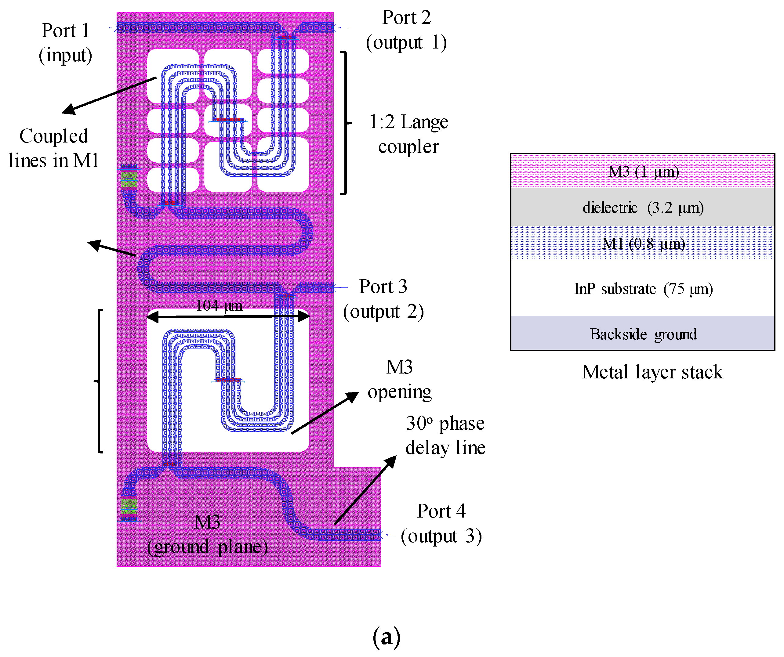
W-band 120° 3-way power divider was required at the input, generating three input signals with 120° phase differences. It was designed by using the 1:2 and 1:1 Lange couplers with phase delay lines, with an electrical length of 30° at
(~ 90 GHz), as illustrated in
Figure 1a. The ratio, 1:2 and 1:1, indicates the power division ratio between the coupled and through ports. These passive components were implemented in the form of inverted microstrip lines, using four frontside metal layers (M1–M4) on the 75 μm-thick InP substrate. The bottom metal layer M1 was used as a signal line and the third metal layer M3 was used as a ground plane. Each metal layer had about 1 μm-thickness, except for the 3 μm-thick M4 (top metal layer). The 1 μm-thick dielectric layers were placed between metal layers. The coupled lines in the Lange couplers were implemented in the M1 layer, where the M3 ground plane was removed (M3 opening in
Figure 2a) in order to increase the coupling factor. On the contrary, the M3 opening was partially connected to reduce the coupling factor in the 1:2 Lange coupler. The 30°-long inverted microstrip lines were inserted to accomplish 120° phase delay, together with 90° phase shift by the Lange coupler. The Lange couplers and phase delay lines were meandered in order to reduce the circuit size.
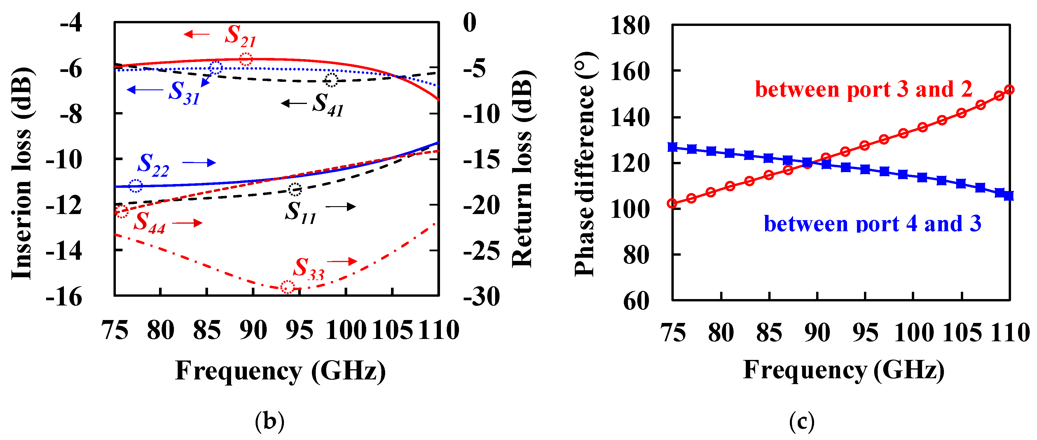
EM simulations were carried out using Advanced Design System (ADS) Momentum from Keysight Technologies to optimize the dimensions of the power dividers, and the results are given in
Figure 2b,c. The designed power divider exhibited almost equal power division and 120° phase difference between three output ports, with good return loss at the center frequency around 90 GHz. The phase error increased as the frequency deviated from the center frequency, which may have limited the bandwidth performance of the frequency tripler. Return loss and isolation were better than 14 dB in the entire
W-band.
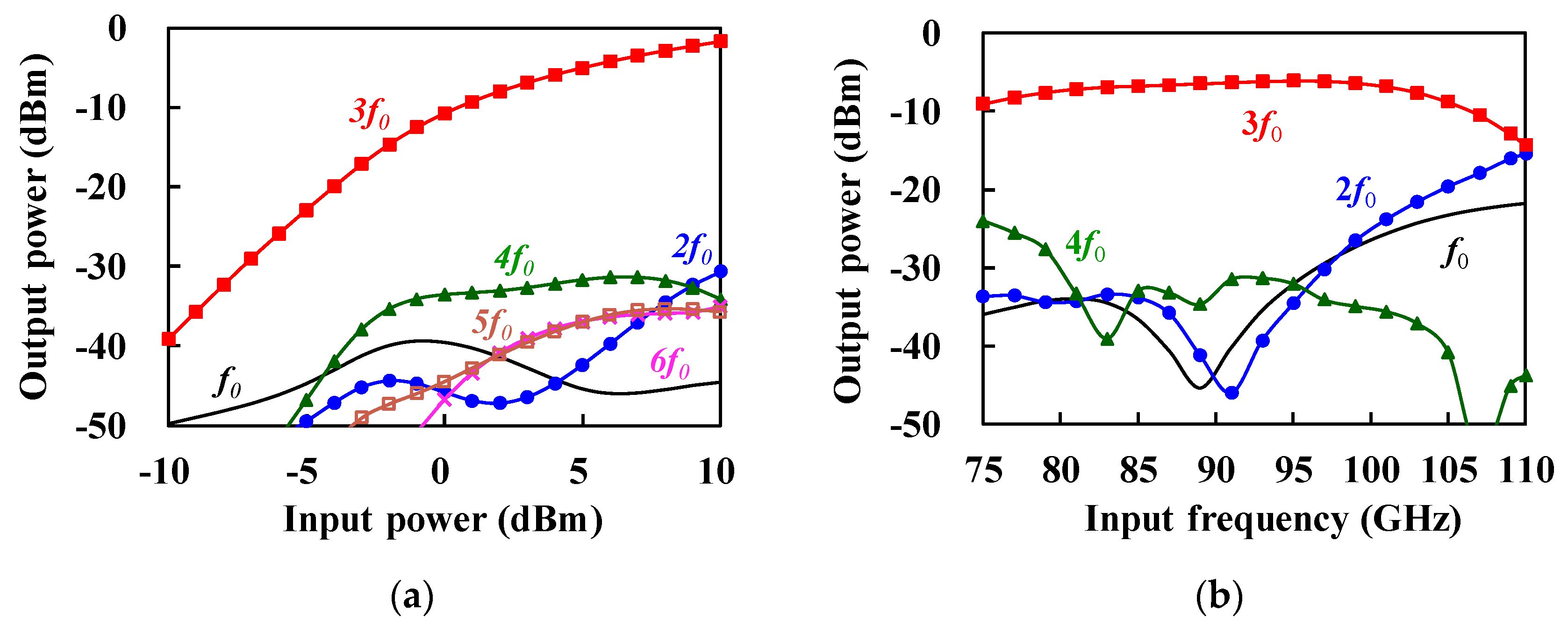
The EM simulation was also performed for the input matching network, combining lines and output matching network, to optimize the performance of the tripler. The designed tripler exhibited a maximum conversion gain of −10.2 dB at an input power of 3.5 dBm at
= 90 GHz, as shown in
Figure 3a.
Figure 3b shows the output power at each harmonic frequency at an input power of 3.5 dBm. It achieves a wideband performance with output power greater than −9.1 dBm (conversion gain >−12.6 dB) at 75 GHz–105 GHz (3 dB bandwidth of conversion gain). It also shows that the fundamental and 2nd harmonic components were sufficiently suppressed by more than 30 dB from 87 to 93 GHz, compared to the 3rd harmonic component, due to the phase cancellation by the triple-push technique.
3. Experimental Results
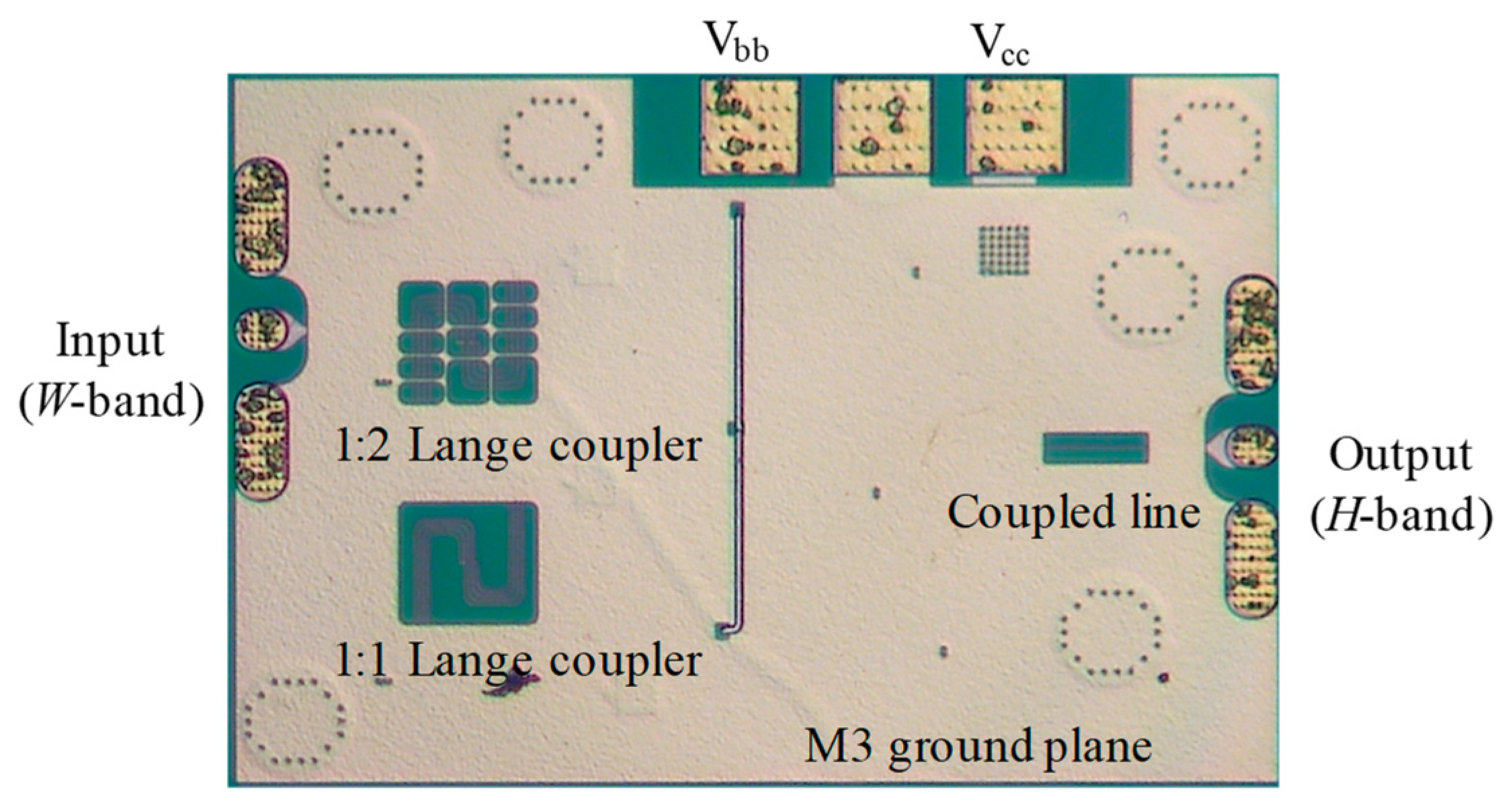
Figure 4 shows the fabricated
H-band frequency tripler in Teledyne Scientific’s 250-nm InP HBT process, which offers high-speed transistors with maximum oscillation frequency (
fmax) around 700 GHz [
2]. The chip size was 790 μm × 535 μm, including direct current (DC) and radio frequency (RF) pads. The performance of the frequency tripler was measured by on-wafer probing, as illustrated in
Figure 5. The
W-band signal (75 GHz–110 GHz) was generated by the frequency multiplier-by-6 module and applied to the chip by a WR-10 waveguide probe. The
H-band output power was measured by using a WR-3.4 waveguide probe (by GGB Industries, Inc. (Naples, FL, USA)) and a
H-band power meter (PM5 by Virginia Diodes, Inc. (Charlottesville, VA, USA)). The loss of each component in the measurement setup (such as the probes and waveguide sections) was measured and calibrated out.
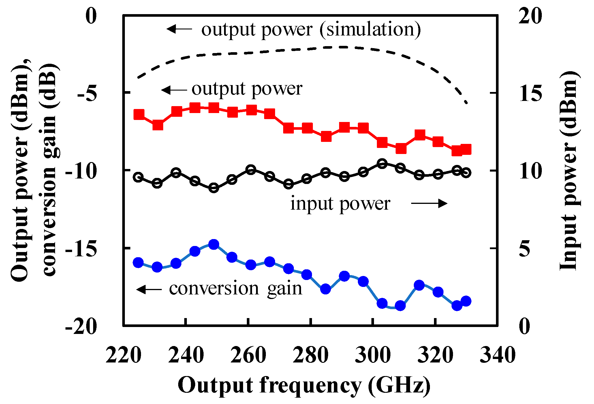
Figure 6 shows the measured output power and conversion gain of the frequency tripler as a function of output frequency at an input power around 9.6 dBm. Measured output power was between −8.8 dBm and −6.0 dBm at 225 GHz–330 GHz, where the conversion gain was between −18.7 dB and −14.8 dB.
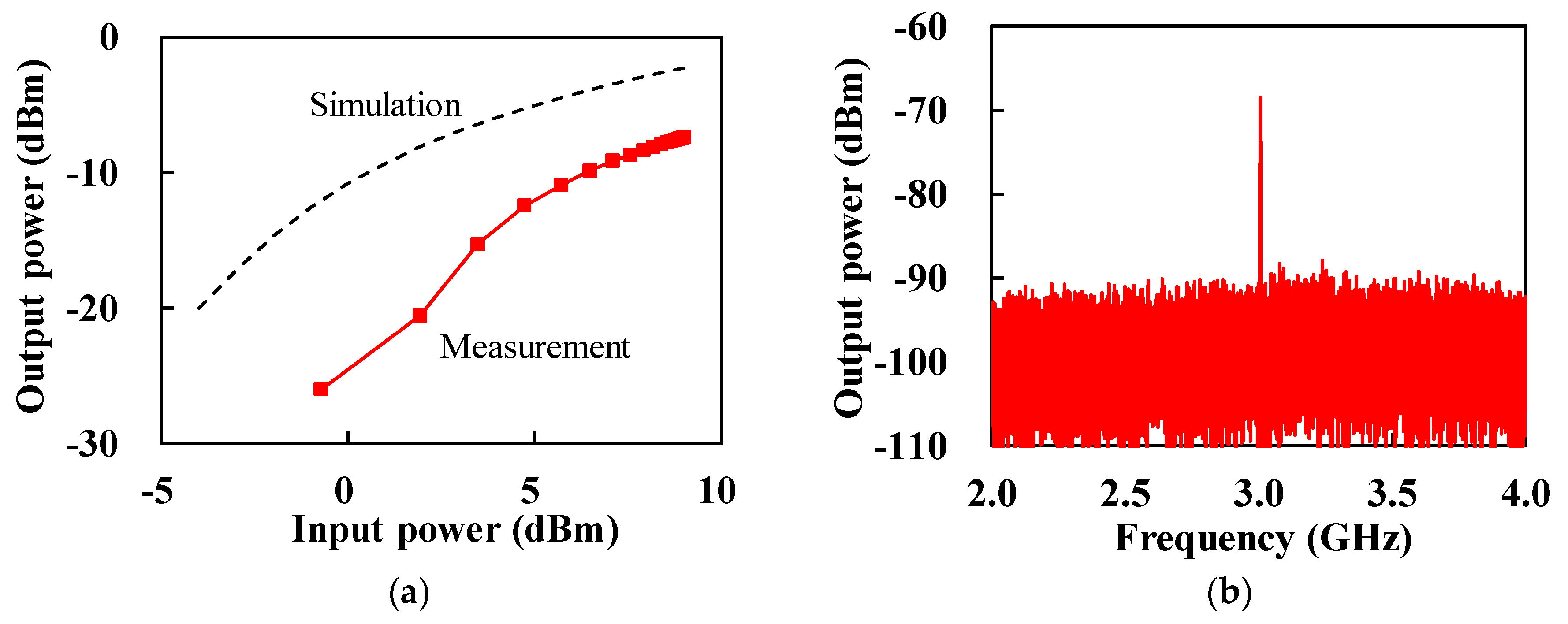
Figure 7 shows the measured output power and spectrum at an input frequency of 91 GHz. As shown in
Figure 7a, there was a discrepancy in the measured and simulated output powers, for example, there was about 6 dB difference at high input power. It was believed to be caused by the inaccurate non-linear model of the transistor at very high frequency provided by the process company. The output spectrum was also on-wafer, measured by down-converting the tripler output signal to low frequency using the
H-band 2nd harmonic mixer,
D-band power source (frequency multiplier-by-12 module) for local oscillator (LO), and spectrum analyzer.
Figure 7b shows the measured down-converted spectrum around 3.0 GHz with a span of 2 GHz, showing a spurious-free output spectrum.
Table 1 compares the performance of active frequency multipliers reported in the
H-band, showing that the frequency tripler designed in this work exhibited a comparable output power and conversion gain with excellent bandwidth performance.

