Article

Compact Double Notch Coplanar and Microstrip Bandstop Filters Using Metamaterial—Inspired Open Ring Resonators

by
Juan Hinojosa
1,
Félix L. Martínez-Viviente
1 and
Alejandro Alvarez-Melcon
2,*
1
Department of Electronics and Computer Engineering, Universidad Politécnica de Cartagena, 30202 Cartagena, Spain
2
Department of Information and Communications Technology, Universidad Politécnica de Cartagena, 30202 Cartagena, Spain
*
Author to whom correspondence should be addressed.
Electronics 2021, 10(3), 330; https://doi.org/10.3390/electronics10030330
Submission received: 28 December 2020 / Revised: 21 January 2021 / Accepted: 28 January 2021 / Published: 1 February 2021
(This article belongs to the Special Issue RF, Microwave and Millimeter Wave Devices and Integrated Systems)

Abstract

:
Compact double notch coplanar and microstrip bandstop filters are described. They are based on a version of the open interconnected split ring resonator (OISRR) integrated in microstrip or coplanar waveguides. The OISRR introduces an RLC resonator connected in parallel with the propagating microstrip line. Therefore, this resonator can be modeled as a shunt circuit to ground, with the R, L and C elements connected in series. The consequence for the frequency response of the device is a notch band at the resonant frequency of the RLC shunt circuit. The number of notch bands can be controlled by adding more OISRRs, since each pair of rings can be modeled as a shunt circuit and therefore introduces an additional notch band. In this paper, we demonstrate that these additional rings can be introduced in a concentric way in the same cell, so the size of the device does not increase and a compact multi-notch bandstop response is achieved, with the same number of notch bands as pairs of concentric rings, plus an additional spurious band at a higher frequency.

1. Introduction

Multi-notch bandstop filters for emerging wireless applications are an important topic of research due to the need for low cost compact solutions that decrease the complexity and size of implementation of communication systems [1]. In this sense, planar technologies such as microstrip or coplanar lines are the preferred options for most applications that do not demand very high-power handling capability. A review of the published literature shows that many solutions have been published for dual-band and tri-band bandpass filters (BPFs). However, most of these designs have relatively large size and high insertion losses, because they are based on several elements inserted in series in the propagation line. Examples of these designs include cascaded stepped-impedance resonators [2,3,4], open stubs filters [5], open loop resonators [6,7], T-shaped resonators [8], and cascaded split-ring resonators [9]. Several design techniques for controlling the resonances by means of even and odd mode analysis [10,11], or the frequency response by using an analysis of the transfer function [12,13], have been proposed. Defected ground structures (DGSs) have also been applied to the design of filters [14,15] to introduce additional resonances and to improve their frequency responses. Analogous situations to the design of multi-band BPFs can be described for multi-notch bandstop filters (BSF) [16,17,18,19,20,21,22], which find important applications in the suppression of spurious signals in communication systems. In the case of the BSF, the insertion losses are lower in the passband as compared to their BPF counterparts. This is due to the resonances of the BSFs taking place in the stopband, rather than in the passband as in the BPFs.
In this paper, we add new concentric rings to a basic open interconnected split ring resonator (OISRR), to achieve additional notch frequencies, thus resulting in a multi-notch response and a simpler design than those proposed in [16,17,18,19,20,21,22]. The open split ring resonator (OSRR) was firstly studied [23,24] and then modified to include interconnected rings [25,26]. Previous works were limited to a pair of rings, but in this paper, we demonstrate that for each new ring that we introduce, a new resonance appears, therefore creating a new notch frequency band. In [27], an example of a three open interconnected split ring resonator (3OISRR) in microstrip technology is described. This design is modified to implement a multi-notch bandstop filter in coplanar technology, thus showing the ability of this resonator to be applied to different planar technologies unlike the other designs presented in [16,17,18,19,20,21,22]. Moreover, losses omitted in previous works are now taken into account in the proposed equivalent circuit model. Each new notch band can be modeled by a shunt RLC circuit to ground with a coupling coefficient that takes into account for the mutual inductance between rings. Hence, the proposed approach allows for the design of multi-notch responses without increasing the size of the device.
We have performed electromagnetic simulations (with HFSS) and circuit simulations (with ADS) of structures with 3OISRR in both microstrip and coplanar waveguides, such as those shown in Figure 1a,b. The 3OISRR cell consists of three open rings of different radii interconnected at a common point of the microstrip or coplanar waveguide. In the case of the microstrip line, an open window is etched on the ground plane to reduce capacitive coupling between the resonator and the ground plane. On the other hand, in the case of the coplanar waveguide, the window is etched on one of the two lateral ground planes, where the 3 rings are placed. As we will see in this article, the three rings of this cell produce two main resonances and a spurious resonance. The first two resonances can be tuned by controlling the dimensions of the rings and they generate the rejection bands of the device. We will describe how these notch bands are influenced by the dimensions of the circuit elements, which can be modeled by a simplified equivalent circuit. Finally, the proposed structures will be fabricated, and their performance will be compared with the electromagnetic simulations to demonstrate the feasibility of the proposed 3OISRR cell.

2. Double Notch Filters Using a 3OISRR Cell in Microstrip and Coplanar Technologies
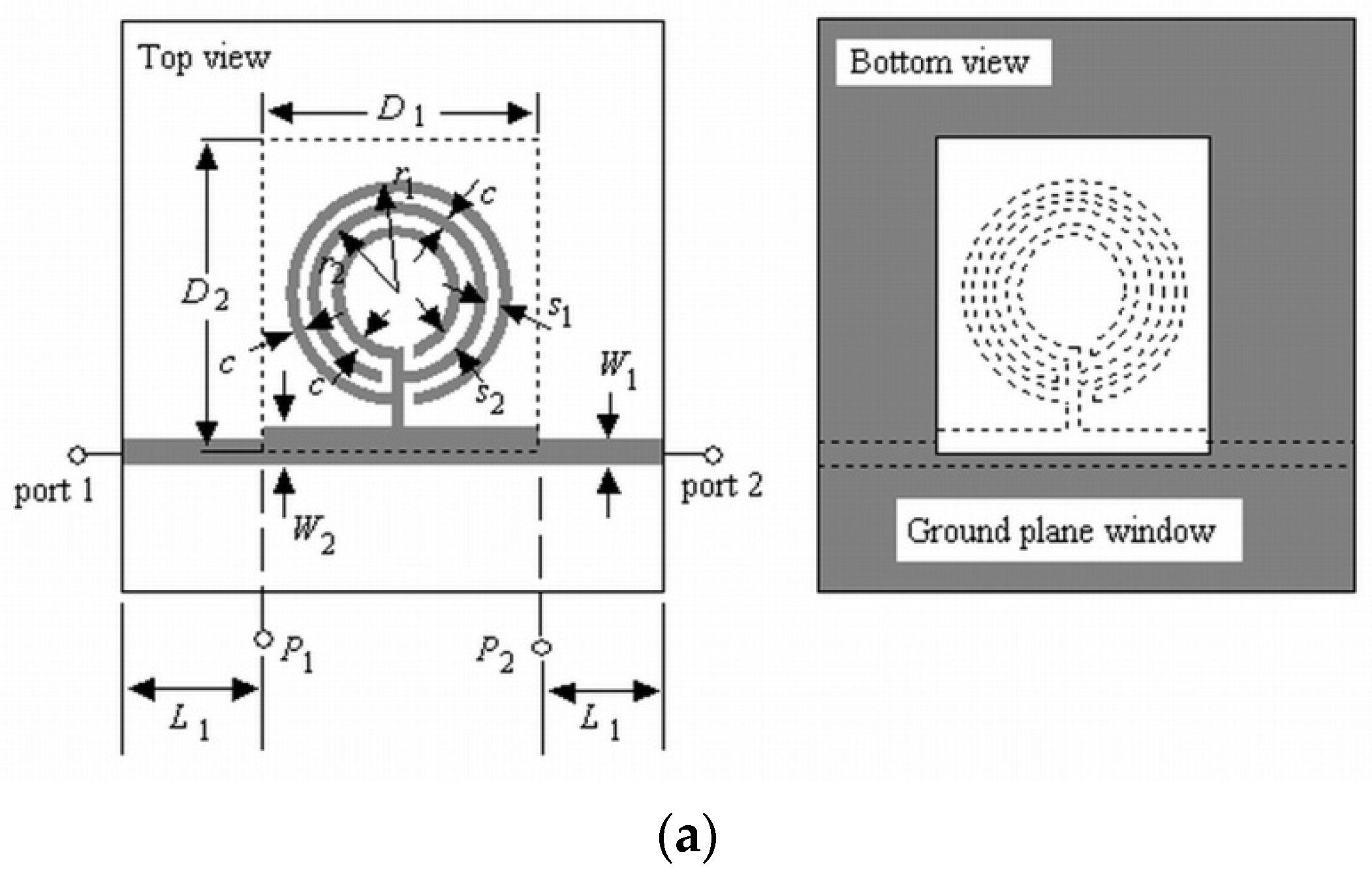
2.1. Structure

The structure of the proposed single cell with three interconnected open split ring resonators and how it is incorporated in a microstrip line or coplanar waveguide is depicted in Figure 1. Since the connection between the three rings and the microstrip or coplanar waveguide is performed at a common point, we can conclude that the insertion of this cell is done in parallel. The dimensions of the different elements of the cell are marked in Figure 1a,b. They are the radii of the external ( r 1 ), central ( r 2 ), and internal rings ( r 3 ), the width c of the rings, the separation s 1 and s 2 between rings, and the length of the sides of the window ( D 1 × D 2 ) etched in the ground plane. The two ground planes of the coplanar waveguide (Figure 1b) are interconnected with via-holes in order to avoid parasitic couplings and the excitation of the even mode of the coplanar waveguide. The width W of the coplanar line is kept constant, while in the case of the microstrip line, the width W is adjusted in order to compensate for the etched window in the ground plane and approximately maintain the same value of characteristic impedance Z c as in the rest of the line.

2.2. Simplified Equivalent Circuit Model
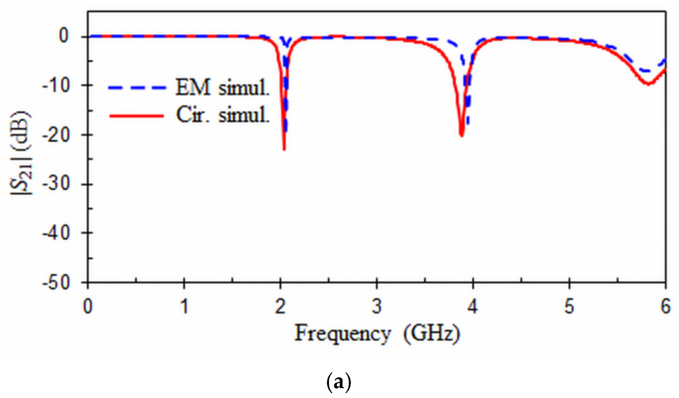
The circuit model for both the coplanar and microstrip cells is shown in Figure 2. Because of the connection to a common point of the three rings, a parallel connection can be assumed in order to derive the circuit model of the filter. Each pair of rings is modeled by a shunt RLC resonant circuit with the resistive, inductive, and capacitive elements in series. A third RLC shunt branch to ground is added to model the spurious rejection band that appears at higher frequencies. Each shunt resonant circuit is connected to ground through a resistance R, which considers the ohmic and radiation losses of the 3OISRR cell in each resonance. The three RLC resonant circuits are placed between the two portions of the propagation line of length d that model the section of the guided wave between points P 1 and P 2 in the structures of Figure 1. Finally, an additional path L 1 of propagation line is included to model the transmission lines between the input and output ports and points P 1 and P 2 , respectively. Note that this equivalent circuit does not take into account higher-order couplings and interactions involved in both structures, and it must be considered as a simplified model that can be used to predict the notch frequencies of the response. An equivalent LC circuit can also be defined by using the approach proposed in [28].
We will call f 0 , 1 and f 0 , 2 the resonant frequencies of the pairs of rings (Figure 1) formed by the external and central rings ( f 0 , 1 ) and the central and internal rings ( f 0 , 2 ), while the spurious frequency will be f 0 , 3 . The three rings of the 3OISRR cell produce two main notch bands centered at f 0 , 1 and f 0 , 2 , and a spurious notch band fixed at f 0 , 3 . Each notch band is modeled by one of the three branches of shunt series RLC circuits shown in Figure 2. A mutual inductance parameter M is introduced to take into account the interaction between the external and internal pair of rings. In order to calculate the values of the parameters of the inductances and capacitances of the circuit model shown in Figure 2, we have proposed an element transformation rule [25] between the open interconnected split ring resonators (OISRR) used in this work and the open split ring resonators (OSRR) of a previous publication [23]. According to this rule, we define the impedance scaling factor γ i as:
γ i = 1 4 × i ( Δ f O S R R ,     i Δ f   0 , i ) ,
where the index i = 1, 2 refers to the external (i = 1) or internal (i = 2) pair of rings. Δ f O S R R or Δ f 0 are the 3 dB bandwidths of the corresponding resonant bands obtained in the electromagnetic simulations for the OSRR and the OISRR equivalent structures. It is worth to note that for the OSRR structure, the resonant band will be a passband, while for the OISRR equivalent structure, the resonance produces a stopband. Hence, once the value of γ i is determined, the values of the inductances and capacitances associated to the OISRRs are calculated from the corresponding values of the same parameters for the equivalent OSRR structure according to the following equations:
L i = γ i L O S R R , i ,
C i = C O S R R , i / γ i .
The values of inductance L O S R R , i and capacitance C O S R R , i for the OSRR structure are calculated from its geometrical dimensions in the following way. L O S R R , i is the inductance of a closed ring of radius equal to the average of the ith and (i + 1)th rings, i.e., r o , i = r i c s / 2 , and the same width c as the considered rings. On the other hand, C O S R R , i is the distributed capacitance of the ith slot between the ith and (i + 1)th rings, which are separated by a distance s i . If we call C p u l , i to the capacitance per unit length of the mentioned slot, then the value of the capacitance is related to the average radius by the equation: C O S R R , i = 2 π r o , i C p u l , i . Once the values of L O S R R , i and C O S R R , i of the equivalent OSRR i circuit [23] have been calculated from the previous considerations, Equations (1)–(3) give us the corresponding values of the OISRR circuit model and only the value of the mutual inductance M remains to be calculated. The value of M is given by the equation:
M = k L 1 L 2 ,
where k is an empirical coupling coefficient.
The shunt series R 3 L 3 C 3 branch is responsible of modeling the spurious frequency notch band. The value of L 3 can be calculated from the 3 dB bandwidth of the spurious stopband Δ f 0 , 3 obtained from the electromagnetic simulations by assuming a 50 Ω terminated two port network and neglecting the effects of the two other shunt circuits. In such case, the following relation can be applied:
x 3 / 50 = f 0 , 3 / ( 2   Δ f 0 , 3 ) L 3 = 50 / ( 4   π   Δ f 0 , 3 ) ,
where x 3 = ω 0 , 3 L 3 is the reactance. The value of the capacitance C 3 follows by simple application of the resonant condition ω 0 , 3 2 = 1 / ( C 3 L 3 ) , and 50 is the reference impedance of the ports.
Finally, the resistance R i that connects each shunt series LC resonant circuit to ground can be computed by means of electromagnetic simulations of the 3OISRR cell using the return loss | S 11 | f 0 , j (obtained at the frequency of resonance f O , j ) and the unloaded quality factor Q u , j :
Q u , j = 2 π f j L j R j = f 0 , j Δ f 0 , j ( 1 | S 11 | f 0 , j ) ,
where the index j = 1, 2, 3 refers to one of the three resonances of the 3OISRR cell.

2.3. Analysis

Figure 3 and Figure 4 present the electromagnetic and circuit simulations of the S 11 and S 21 parameters for a 3OISRR cell excited by means of microstrip and coplanar waveguides. The geometrical dimensions of the 3OISRR cell are: r 1 = 2.2 mm, r 2 = 1.65 mm, r 3 = 1.1 mm, c = 0.3 mm, and s 1 = s 2 = 0.25 mm both for the microstrip and coplanar structures. The dimensions of the open window are, respectively, D 1 × D 2 = 9 × 9 mm2 and D 1 × D 2 = 9 × 6.5 mm2 for the microtrip and coplanar waveguides. Values of other parameters needed for the simulations are: copper thickness t = 17.5 μm, substrate thickness h = 0.635 mm, substrate permittivity ε r = 10.2, L 1 = 5.5 mm, W 1 = 0.594 mm, W 2 = 0.794 mm, W = 0.374 mm, S = 0.163 mm, and Z c = 50   . Analogous simulations for equivalent OSRR structures give the values of Δ f O S R R , i , which allow to calculate the factor γ i of Equation (1). These values and the elements L O S R R , i and C O S R R , i calculated as explained before are summarized in Table 1. It should be noted that the data and the factor γ i included in Table 1 for the first and second resonators are the same for the microstrip and coplanar waveguides. Once the factor γ i is known, the values of L i and C i for the first and second resonators can be calculated from Equations (2) and (3). The factor k that appears in the mutual inductance of the Equation (4) was empirically obtained by an optimization procedure between circuit and electromagnetic simulations, resulting in the value k = 0.51. The values of the elements of the equivalent circuit for the spurious resonator have also been calculated following the procedure presented above. Finally, the value of the quality factor Q u , j of each resonator for microstrip and coplanar waveguides has been computed by means of the Equation (6) and from the values f O , i and Δ f O , i obtained from electromagnetic simulations (Figure 3 and Figure 4). Data and the equivalent circuit elements of Figure 2 for microstrip and coplanar waveguides are presented in Table 2 and Table 3, respectively. It should be noted in these tables that the element values of the equivalent circuit for the first and second resonators are the same for the microstrip and coplanar structures, since they only depend on the geometry of the 3OISRR cell. However, the element values of the third (spurious) resonator are different when the cell is inserted in the microstrip or coplanar waveguide. This is due to the influence of the surrounding elements (ground plane, via holes, etc…) on the frequency of this spurious resonance.
As it can be seen in Figure 3 and Figure 4, a reasonable agreement is obtained between the electromagnetic and circuit simulations. We observe that both the microstrip and coplanar structures present the first two resonances at exactly the same frequencies: f O , 1 = 2 GHz and f O , 1 = 3.9 GHz. Hence, it is concluded that these resonances depend only on the geometry of the 3OISRR cell. The narrow bandwidth of these resonances indicates that they are notch bands. The coplanar structure presents quality factors (Table 3) higher than the microstrip structure (Table 2). These values are higher than 173 for the first two resonances in both structures. With regard to the third (spurious) resonance, it appears at a different frequency for the microstrip ( f O , 3 = 5.8 GHz) and coplanar ( f O , 3 = 5.1 GHz) structure. Its 3 dB bandwidth ( Δ f 0 , 3 = 0.6 GHz for the microstrip line and Δ f 0 , 3 = 0.4 GHz for the coplanar waveguide) is much higher than for the notch bands. Additionally, considering the low values of the return losses ( | S 11 | f 0 , 3 = 6.4 dB for the microstrip line and | S 11 | f 0 , 3 = 3.6 dB for the coplanar waveguide) and that this resonance is observed at approximately two times the frequency ( f 0 , 1 + ( f 0 , 2 f 0 , 1 ) / 2 ) , all this information indicates that it is a spurious resonance.
The responses of the microstrip and coplanar structures exhibit three transmission zeros at the resonant frequencies of the 3OISRR cell, since an electric short to ground occurs at these frequencies, which reflects the injected power back to the source. The microstrip and coplanar structures loaded with the 3OISRR cell behave as three shunt series RLC resonant circuits embedded between two microstrip and coplanar line sections. In addition to these resonances, anti-resonances (Figure 3) also appear. The microstrip structure (Figure 3a) has two anti-resonances around f O , 1 and a third one above f O , 2 . The first anti-resonance below f O , 1 is as a consequence of the matching between the 3OISRR cell and the ports, while the second and third ones above f O , 1 and f O , 2 occur due to the anti-resonant behavior of the effective permittivity of the 3OISRR cell [29]. On the other hand, in the case of the coplanar structure (Figure 3b), only the anti-resonances above f O , 1 and f O , 2 can be observed. This is because the width W of the coplanar line is not adjusted to compensate the etched window in the ground plane. Therefore, the ports do not show a frequency of perfect match below f O , 1 . At each anti-resonance above f O , 1 and f O , 2 , the microstrip and coplanar structures loaded with the 3OISRR cell behave as a shunt parallel RLC resonant circuit. The differences between the circuit and electromagnetic simulations are due to the fact that the equivalent circuit presented in Figure 2 does not consider higher-order couplings and interactions that occur in both structures. The equivalent circuit must be used as a simplified model to obtain the response trends of the microstrip and coplanar structures loaded with a 3OISRR cell and to predict the notch frequencies.
In order to analyze these resonances in more detail, we have studied the current distributions by means of electromagnetic simulations at representative frequencies for both microstrip and coplanar structures. The first frequency (Figure 5a) is inside the pass band ( f = 1 GHz). At this frequency, the 3OISRR cell does not resonate, and the signal is transmitted from the input to the output port. At the second frequency (Figure 5b), inside the notch band corresponding to the first resonance ( f 0 , 1 = 2 GHz), we observe a strong resonance between the central ring and the external and internal rings. This resonance completely blocks the transmission of the signal between the input and output ports. The third simulation frequency (Figure 5c) is inside the notch band, corresponding to the second resonance ( f 0 , 2 = 3.9 GHz). In this case, the simulations show that the resonance occurs between the central and inner rings, which avoids the transmission of the signal between the input and output ports. The fourth frequency (Figure 5d) corresponds to the spurious band ( f 0 , 3 = 5.8 GHz for the microstrip structure and f 0 , 3 = 5.1 GHz for the coplanar structure). As remarked above, this band can be recognized by its larger bandwidth. In Figure 5d, we also see that the resonance is weak and some signal passes through the structure. This can also be appreciated in Figure 3 and Figure 4, where the electromagnetic simulations (dash lines) show a much less pronounced maximum for the S 11 parameter (or minimum for S 21 ) at the spurious frequencies. The fifth frequency (Figure 5e) is the anti-resonance below f 0 , 1 for the microstrip structure, which occurs at f = 1.7 GHz. The simulation displays a residual current on the first half of the external ring, and the signal is transmitted from the input to the output port (due to a perfect matching condition with the ports). Finally, the sixth (Figure 5f) and seventh (Figure 5g) frequencies correspond to the anti-resonances above f 0 , 1 ( f a , 1 = 2.5 GHz for the microstrip structure and f a , 1 = 2.07 GHz for the coplanar structure) and f 0 , 2 ( f a , 2 = 4.5 GHz for the microstrip structure and f a , 2 = 4.3 GHz for the coplanar structure). In Figure 5f,g, we observe that the 3OISRR cell resonate for both anti-resonances. However, unlike the cases of the first (Figure 5b) and second (Figure 5b) resonances, the signal is transmitted between the input and output ports, thus showing that at these resonant frequencies the microstrip and coplanar structures loaded with the 3OISRR cell no longer behave as a shunt series RLC resonant circuit but rather as a shunt parallel RLC resonant circuit.
We can summarize the electromagnetic and circuit simulation results by remarking that the 3OISRR cell performs as a double notch filter for the first two resonant frequencies, whose values do not depend on whether the structure is inserted in a microstrip or coplanar waveguide. These two notched bands are achieved by means of a simple 3OISRR cell without cascading several stages of stepped-impedance resonators stub-loaded resonators, Hilbert-fork resonators, or hexagonal split ring resonators, a significant advantage when compared with previous work with multi-notch filters [16,17,18,19,20,21]. Instead of cascaded stages, our novel structure achieves the same effect with a single cell of three open rings of different radii interconnected to a common point of the microstrip or coplanar waveguide. The first two resonances can be controlled by adjusting the radii of the 3OISRR cell as described in the previous sub-section. If we analyze the electric size of the cell at the two resonant frequencies, we observe that at the first resonance ( f O , 1 = 2 GHz), the 3OISRR presents half the electric size of the equivalent SRR cell. At the second resonance ( f O , 2 = 3.9 GHz), the guided wavelengths in the microstrip and coplanar waveguides are, respectively, λ = 30 mm and λ = 34 mm which have been calculated from the corresponding effective permittivity ε r e f = 6.4 and ε r e f = 5 . In comparison, the length D 1 of the proposed 3OISRR structure is only 9 mm, which is less than λ/3, thus confirming that the proposed 3OISRR is more compact than a conventional resonator with a length of λ/2.

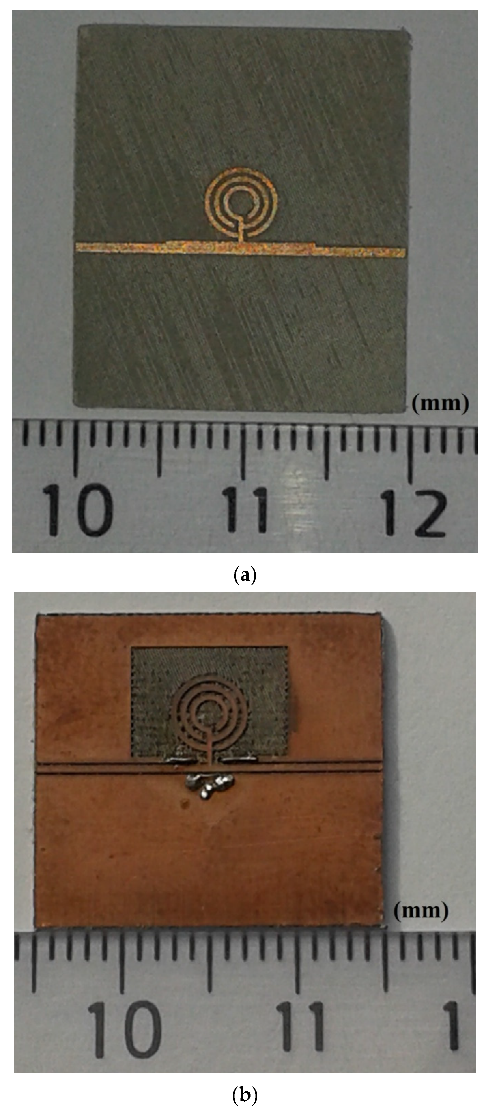
3. Fabrication and Results

In order to experimentally demonstrate the feasibility of the proposed concept, we have fabricated the structures of Figure 1 using a substrate of Arlon material (AD1000) with the following parameters: ε r = 10.2 , tg δ = 0.0023 at 10 GHz, thickness h = 0.635 mm, and copper metallization thickness t = 17.5 µm. A laser prototyping system (LPKF Protolaser S) was used for the manufacturing of the structures, and the results of these fabrication processes are shown in Figure 6. The experimental testing was carried out by means of a Rohde & Schwarz ZVA network analyzer and a test fixture Anritsu 3680K. The calibration and measurements were done in the frequency range between 0.01 and 6 GHz.
Figure 7 and Figure 8 depict, respectively, the measurements of the S 11 and S 21 parameters for both microstrip and coplanar structures. The results of the electromagnetic simulations are also added for validation. As it can be seen, a reasonable agreement between electromagnetic simulations and measurements is achieved. For easy comparison with the electromagnetic simulation results (Table 2 and Table 3), we present the measurement results in Table 4 and Table 5. These tables also include the insertion losses | S 21 | f 0 , j in the stop bands for the first, second, and third (spurious) resonances. In the same way as with the electromagnetic simulated results, the quality factor decreases as the resonant frequency increases. For both structures, their values are higher than 132, 78, and 50 for the first, second, and third resonance, respectively. Higher quality factors are obtained with the coplanar notch filter. However, the insertion loss in the pass bands is better for the microstrip filter. For example, at 2.5 GHz, the passband insertion loss for the microstrip filter is 0.06 dB, while it is 0.35 dB for the coplanar filter. As it can be seen in Figure 7 and Figure 8, the spurious band appears above 5 GHz for both microstrip and coplanar structures. The 3OISRR cell opens the possibility to generate compact bandstop responses with two notched bands without increasing the size of the circuit, just by adding a new ring to the OISRR cell. Hence, the number of main resonances, and therefore notch bands, is the number of rings minus one, since the spurious band cannot be controlled independently from the main resonances with the parameters of the rings.
Finally, Table 6 compares different multi-band bandstop filters with the proposed double notch filters. In this table, f i , F B W i , and R L S i represents, respectively, the central resonant frequency of the ith-stopband, the 3 dB fractional bandwidth of the ith-stopband, and the maximum rejection level at the central ith-stopband. λ 0 corresponds to free-space wavelength at the central frequency of the multi-band bandstop filters. It is defined to assess the 2D size of the different filters. As it can be seen in Table 6, the proposed filters present some of the lowest resonant frequencies at the first stopband, except for the designs presented in [16,17] (Figure 8), although these ones have a very large fractional bandwidth ( F B W i > 50 % ) . The structures defined in [20,22] have a fractional bandwidth and a maximum rejection level similar to the proposed filters. However, both structures present a second transmission zero very close to the first one. In addition, their maximum rejection levels at the second stopband are worse than the proposed structures. In terms of size, the proposed double notch filters are more compact than any other design. The proposed 3OISRR cell has significant advantages compared with previous works [16,17,18,19,20,21,22], which require complex structures or cascading several stages. Its structure is simpler and versatile, since the transmission zeros are controlled by adjusting the radii of the rings and it can be connected to different planar technologies (microstrip, coplanar). Moreover, it is easier to introduce an additional notch. It is enough to add an additional ring in the same cell.

4. Conclusions

We have presented compact bandstop filters with two-notched bands in coplanar and microstrip technologies based on the concept of adding multiple rings to an open interconnected split ring resonator (OISRR) cell. In particular, the proposed structures use a 3OISRR cell with 3 open rings of different radii connected to a common point of the microstrip or coplanar waveguide. The frequency response of these filters presents two main resonances and a spurious resonance at higher frequencies. There are no significant differences between the coplanar and microstrip structures in the main resonance frequencies. Both structures present insertion loss and 3 dB notch bandwidth for the first resonance lower than 8.3 dB and 0.04 GHz, while for the second resonance these are, respectively, lower than 17.2 dB and 0.6 GHz. The best results are achieved for the coplanar structure, since the experimental measurements show unloaded quality factors higher than for the microstrip structure. The proposed 3OISRR cell have a reduced size ( < λ / 3 ) as compared with λ / 2 conventional resonators. Therefore, these multi-notch bandstop filters can be expected to be of interest to reduce unwanted signals in future communication systems.

Author Contributions

J.H. has analyzed, designed, fabricated and measured the double notch coplanar and microstrip bandstop filters. F.L.M.-V. has provided a great assistance during the different phases of this work (analysis, design and fabrication) and wrote the manuscript. A.A.-M. has also contributed in the analysis and design of these notch filters and participated in manuscript revision. All authors have read and agreed to the published version of the manuscript.

Funding

The authors gratefully acknowledge financial support from Agencia Estatal de Investigación (AEI) of Spain (grant no.: PID2019-103982RB-C42/AEI/10.13039/ 501100011033).

Conflicts of Interest

The authors declare no conflict of interest.

References

  1. Hong, J.S.; Lancaster, M.J. Microstrip Filters for RF/Microwave Applications; John Wiley & Sons: New York, NY, USA, 2001. [Google Scholar]
  2. Wei, F.; Li, W.T.; Shi, X.W.; Huang, Q.L. Compact UWB bandpass filter with triple-notched bands using triple-mode stepped impedance resonator. IEEE Microw. Wirel. Compon. Lett. 2012, 22, 512–514. [Google Scholar] [CrossRef]
  3. Hou, Z.; Liu, C.; Zhang, B.; Song, R.; Wu, Z.; Zhang, J.; He, D. Dual-/tri-wideband bandpass filter with high selectivity and adjustable passband for 5G mid-band mobile communications. Electronics 2020, 9, 205. [Google Scholar] [CrossRef] [Green Version]
  4. Lalbakhsh, A.; Ghaderi, A.; Mohyuddin, W.; Simorankir, R.B.V.B.; Bayat-Makou, N.; Ahmad, M.S.; Lee, G.H.; Kim, K.W. A compact C-band bandpass filter with an adjustable dual-band suitable for satellite communication systems. Electronics 2020, 9, 1088. [Google Scholar] [CrossRef]
  5. Wei, X.B.; Wang, P.; Gao, P.; Xu, Z.Q.; Liao, J.X.; Jin, L.; Shi, Y. Compact tri-band bandpass filter using open stub loaded tri-section λ/4 stepped impedance resonator. IEEE Microw. Wirel. Compon. Lett. 2014, 24, 512–514. [Google Scholar] [CrossRef]
  6. Pal, M.; Chatterjee, J.; Ghatak, R. Multiband BPF with wide upper stop band using asymmetrically positioned stub loaded open loop resonators. AEU Int. J. Electron. Commun. 2014, 68, 1041–1046. [Google Scholar] [CrossRef]
  7. Ibrahim, A.A.; Ali, W.A.E.; Abdelghany, M.A. Design of dual-band dual-mode band-pass filter utilizing 0° feed structure and lumped capacitors for WLAN-WiMax applications. Electronics 2020, 9, 1697. [Google Scholar] [CrossRef]
  8. Lalbakhsh, A.; Alzadeh, S.M.; Ghaderi, A.; Golestanifar, A.; Mohamadzade, B.; Jamshidi, M.; Mandal, K.; Mohyuddin, W. A design of a dual-band bandpass filter based on modal analysis for modern communication systems. Electronics 2020, 9, 1770. [Google Scholar] [CrossRef]
  9. Geschke, R.H.; Jokanovic, B.; Meyer, P. Filter parameter extraction for triple-band composite split-ring resonators and filters. IEEE Trans. Microwave Theory Tech. 2011, 59, 1500–1508. [Google Scholar] [CrossRef]
  10. Karimi, G.; Amiriam, M.; Ranjbar, M. A new microstrip coupling system for realization of a differential dual-band bandpass filter. AEU Int. J. Electron. Commun. 2019, 99, 186–192. [Google Scholar] [CrossRef]
  11. Fan, M.; Song, K.; Zhu, Y.; Fan, Y. Compact bandpass-to-bandstop reconfigurable filter with wide tuning range. IEEE Microw. Wirel. Compon. Lett. 2019, 29, 198–200. [Google Scholar] [CrossRef]
  12. Lalbakhsh, A.; Jamshidi, M.B.; Siakamari, H.; Ghaderi, A.; Golestanifar, A.; Linhart, R.; Talla, J.; Simorangkir, R.B.V.B.; Mandal, K. A compact lowpass filter for communication systems based on transfer function analysis. AEU Int. J. Electron. Commun. 2020, 124, 153318. [Google Scholar] [CrossRef]
  13. Karimi, G.; Siahkamari, H.; Hamedani, F.K.; Lalbakhsh, A. Design of modified Z-shaped and T-shaped microstrip filter based on transfer function analysis. Wirel. Pers Commun. 2015, 82, 2005–2016. [Google Scholar] [CrossRef]
  14. Ahmadi, A.; Makki, S.V.; Lalbakhsh, A.; Majidifar, S. A novel dual-mode wideband band pass filter. Appl. Comp. Electro. Soc. J. 2014, 29, 735–742. [Google Scholar]
  15. Chen, H.; Jiang, D.; Chen, X. Wideband bandstop filter using hybrid/CPW-DGS with via-hole connection. Electron. Lett. 2016, 52, 1469–1470. [Google Scholar] [CrossRef]
  16. Chin, K.S.; Yeh, J.H.; Chao, S.H. Compact dual-band bandstop filters using stepped-impedance resonators. IEEE Microw. Wirel. Compon. Lett. 2007, 17, 849–851. [Google Scholar] [CrossRef]
  17. Gao, L.; Cai, S.W.; Zhang, X.Y.; Xue, Q. Dual-band bandstop filter using open and short stub-loaded resonators. In Proceedings of the International Conference on Microwave and Millimeter Wave technology (ICMMT), Shenzhen, China, 5–8 May 2012; pp. 1–3. [Google Scholar]
  18. Wei, F.; Wang, Z.D.; Yang, F.; Shi, X.W. Compact UWB BPF with triple-notched bands based on stub loaded resonator. Electron. Lett. 2013, 49, 124–125. [Google Scholar] [CrossRef]
  19. Jankovic, N.; Geschke, R.; Crnojevi´c-Bengin, V. Compact tri-band bandpass and bandstop filters based on hilbert-fork resonators. IEEE Microw. Wirel. Compon. Lett. 2013, 23, 282–284. [Google Scholar] [CrossRef]
  20. Fertas, K.; Ghanem, F.; Challal, M.; Ouahdi, M.; Fertas, F.; Aksas, R. Design and implementation of a novel tri-band bandstop filter based on hexagonal metamaterials split ring resonators. In Proceedings of the 2017 5th International Conference on Electrical Engineering-Boumerdes (ICEE-B), Boumerdes, Algeria, 29–31 October 2017; IEEE: Piscataway, NJ, USA, 2017. [Google Scholar]
  21. Zheng, X.; Jiang, T. Triple notches bandstop microstrip filter based on arhimedean spiral electromagnetic bandgap structure. Electronics 2019, 8, 964. [Google Scholar] [CrossRef] [Green Version]
  22. Wang, J.; Zhao, J.; Li, J.L. Compact UWB bandpass filter with triple notched bands using parallel U-shaped defected microstrip structure. Electron. Lett. 2014, 50, 89–91. [Google Scholar] [CrossRef]
  23. Martel, J.; Marqués, R.; Falcone, F.; Baena, J.D.; Medina, F.; Martin, F.; Sorolla, M. A new LC series element for compact bandpass filter design. IEEE Microw. Wireless Compon. Lett. 2004, 24, 210–212. [Google Scholar] [CrossRef]
  24. Vélez, A.; Aznar, F.; Durán-Sindreu, M.; Bonache, J.; Martín, F. Stop-band and band-pass filters in coplanar waveguide technology implemented by means of electrically small metamaterial-inspired open resonators. IET Microw. Antennas Propag. 2010, 4, 712–716. [Google Scholar] [CrossRef]
  25. Ruiz, J.D.; Hinojosa, J.; Alvarez-Melcon, A. Microstrip notch filters based on open interconnected split ring resonators (OISRRs). Appl. Phys. A 2013, 112, 263–267. [Google Scholar] [CrossRef]
  26. Ruiz, J.D.; Hinojosa, J. Shunt series LC circuit for compact coplanar waveguide notch filter design. IET Microw. Antennas Propag. 2014, 8, 125–129. [Google Scholar] [CrossRef]
  27. Hinojosa, J.; Martínez-Viviente, F.L.; Ruiz, J.D.; Alvarez-Melcon, A. Modified split-ring resonator for microstrip dual-band notch filter. In Proceedings of the European Microwave Conference (EuMC), Paris, France, 7–10 September 2015; pp. 813–816. [Google Scholar]
  28. Karimi, G.; Lalbakhsh, A.; Dehghani, K.; Siahkamari, H. Analysis of novel approach to design of ultra-wide stopband microstrip low-pass filter using modified U-shaped resonator. ETRI J. 2015, 37, 945–950. [Google Scholar] [CrossRef]
  29. Koschny, T.; Markos, P.; Smith, D.R.; Soukoulis, C.M. Resonant and anti-resonant frequency dependence of the effective parameters of metamaterials. Phys. Rev. E 2003, 68, 656021. [Google Scholar] [CrossRef] [Green Version]
Figure 1. Double notch filters implemented by means of 3OISRR cells in (a) microstrip technology and (b) coplanar technology.
Electronics 10 00330 g001aElectronics 10 00330 g001b
Figure 2. Simplified equivalent circuit of the 3OISRR cell for both the microstrip and coplanar structures shown in Figure 1.
Electronics 10 00330 g002
Figure 3. Equivalent circuit (solid line) and Electromagnetic (EM) (dashed line) simulations for the S11 parameter of the 3OISRR cell inserted in (a) a microstrip line and (b) a coplanar waveguide.
Electronics 10 00330 g003
Figure 4. Equivalent circuit (solid line) and EM (dashed line) simulations for the S21 parameter of the 3OISRR cell inserted in (a) a microstrip line and (b) a coplanar waveguide.
Electronics 10 00330 g004aElectronics 10 00330 g004b
Figure 5. Current distributions of the 3OISRR cell inserted in a microstrip line (left) and a coplanar waveguide (right) at (a) below resonances f = 1 GHz; (b) first resonance f 0 , 1 ; (c) second resonance f 0 , 2 ; (d) third resonance f 0 , 3 ; (e) anti-resonance for microstrip structure below f 0 , 1 ; (f) first anti-resonance above f 0 , 1 ; (g) second anti-resonance above f 0 , 2 .
Electronics 10 00330 g005aElectronics 10 00330 g005b
Figure 6. Photographs of the fabricated double notch bandstop filters based on a 3OISRR cell inserted in (a) a microstrip line and (b) a coplanar waveguide.
Electronics 10 00330 g006
Figure 7. Comparison of EM simulation (dashed line) and experimental measurement (solid line) for the S 11 parameter of the 3OISRR cell inserted in (a) a microstrip line and (b) a coplanar waveguide.
Electronics 10 00330 g007
Figure 8. Comparison of EM simulation (dashed line) and experimental measurement (solid line) for the S 21 parameter of the 3OISRR cell inserted in (a) a microstrip line and (b) a coplanar waveguide.
Electronics 10 00330 g008aElectronics 10 00330 g008b
Table 1. Data and factor γ i .
Parameter of Resonator 1
(for Microstrip and CPW)
Parameter of Resonator 2
(for Microstrip and CPW)
L o S R R , 1 (nH)7.3 L o S R R , 2 (nH)4.6
C o S R R , 1 (pF)0.7 C o S R R , 2 (pF)0.6
Δ f o S R R , 1 (GHz)2.15 Δ f o S R R , 2 (GHz)3
Δ f 0 , 1 (GHz)0.025 Δ f 0 , 2 (GHz)0.15
γ 1 21.5 γ 2 2.5
Table 2. Electromagnetic simulation results and element values of the equivalent circuit (Figure 2) for the microstrip structure.
Microstrip
f 0 , 1 2 f 0 , 2 3.9 f 0 , 3 5.8
| S 11 | f 0 , 1 −4.2 | S 11 | f 0 , 2 −1.4 | S 11 | f 0 , 3 −6.4
Q u , 1 173 Q u , 2 174 Q u , 3 19
R 1 11.4 R 2 1.6 R 3 12.6
L 1 156.9 L 2 11.5 L 3 6.6
C 1 0.032 C 2 0.24 C 3 0.11
where f 0 , i , | S 11 | f 0 , i ,   R i , L i , and C i (i = 1, 2, and 3) are respectively in GHz, dB, , nH, and pF.
Table 3. Electromagnetic simulation results and element values of the equivalent circuit (Figure 2) for the coplanar structure.
Coplanar
f 0 , 1 2 f 0 , 2 3.9 f 0 , 3 5.1
| S 11 | f 0 , 1 −0.5 | S 11 | f 0 , 2 −0.8 | S 11 | f 0 , 3 −3.6
Q u , 1 1191 Q u , 2 295 Q u , 3 37
R 1 1.6 R 2 0.95 R 3 8.5
L 1 156.9 L 2 11.5 L 3 9.9
C 1 0.032 C 2 0.24 C 3 0.09
where f 0 , i , | S 11 | f 0 , i ,   R i , L i , and C i (i = 1, 2, and 3) are respectively in GHz, dB, , nH, and pF.
Table 4. Measurement results for the microstrip structure.
Microstrip
f 0 , 1 2.11 f 0 , 2 3.96 f 0 , 3 5.8
Δ f 0 , 1 0.04 Δ f 0 , 2 0.3 Δ f 0 , 3 0.5
| S 11 | f 0 , 1 −4.4 | S 11 | f 0 , 2 −1.6 | S 11 | f 0 , 3 −2.3
| S 21 | f 0 , 1 −8.3 | S 21 | f 0 , 2 −17.2 | S 21 | f 0 , 3 −14.5
Q u , 1 132 Q u , 2 78 Q u , 3 50
where f , Δ f , and | S | are respectively in GHz, GHz, and dB.
Table 5. Measurement results for the coplanar structure.
Coplanar
f 0 , 1 2.04 f 0 , 2 3.85 f 0 , 3 5.1
Δ f 0 , 1 0.04 Δ f 0 , 2 0.6 Δ f 0 , 3 0.5
| S 11 | f 0 , 1 −2.5 | S 11 | f 0 , 2 −0.7 | S 11 | f 0 , 3 −1.9
| S 21 | f 0 , 1 −11.2 | S 21 | f 0 , 2 −23.6 | S 21 | f 0 , 3 −15.7
Q u , 1 204 Q u , 2 83 Q u , 3 52
where f , Δ f , and | S | are respectively in GHz, GHz, and dB.
Table 6. Comparison of the proposed double notch filters with other reported multi-band bandstop filters.
Ref. f 1 / f 2 / ( GHz ) F B W 1 / F B W 2 / ( % ) R L S 1 / R L S 2 / ( dB ) 2D Size
λ 0 × λ 0
[16] Figure 5a1.57/3.1656.7/28.246/54 0.198 × 0.198
[17] Figure 72.89/54.8/528/16 0.394 × 0.223
[17] Figure 81.16/3.550/14.329/28 0.269 × 0.203
[18] Figure 43.6/5.9/82.9/3.7/2.315/15/10 0.353 × 0.196
[19] Figure 62.36/3.48/5.193.6/2.5/2.814.4/26.3/34.63 0.267 × 0.115
[20] Figure 106.1/6.9/7.62.3/5.2/1.715/14/13 1.023 × 0.279
[21] Figure 14b3.5/5.2/7.415.6/7.8/8.935.6/28.2/24.9 0.509 × 0.218
[22] Figure 45.2/5.8/81.8/2.3/2.117/16/15 0.4 × 0.266
This work Figure 8a2.11/3.961.9/7.68.3/17.2 0.102 × 0.102
This work Figure 8b2.04/3.851.9/15.611.2/23.6 0.1 × 0.1
Publisher’s Note: MDPI stays neutral with regard to jurisdictional claims in published maps and institutional affiliations.

