Article

Light-Load Efficiency Optimization for an LCC-Parallel Compensated Inductive Power Transfer Battery Charger

1
School of Energy and Power Engineering, Wuhan University of Technology, Wuhan 430063, China
2
School of Automation, Wuhan University of Technology, Wuhan 430070, China
*
Author to whom correspondence should be addressed.
Electronics 2020, 9(12), 2080; https://doi.org/10.3390/electronics9122080
Submission received: 27 October 2020 / Revised: 27 November 2020 / Accepted: 3 December 2020 / Published: 6 December 2020
(This article belongs to the Section Power Electronics)

Abstract

:
Wireless power transfer (WPT) techniques have gained wide acceptance across a range of battery charging applications such as cell phones, cardiac pacemakers, and electric vehicles. In a wireless battery charging system, a constant current/constant voltage (CC/CV) charging strategy, regardless of the variation of the battery load which may roughly range from a few ohms to several hundred ohms, is typically adopted to ensure the safety, durability, and performance of the battery. However, system efficiency drops significantly as the load increases in CV mode, especially at very light-load conditions. This paper proposes an efficiency optimization method for an LCC-parallel compensated inductive power transfer (IPT) battery charging system without the help of any additional power converter and control method. The equivalent circuit and resonant conditions of the LCC-parallel compensation topology are firstly analyzed to achieve the load-independent CV output at a zero phase angle (ZPA) operating frequency. Over the full range of CV charging mode, the efficiency of the LCC-parallel resonant tank circuit is analyzed and optimized. An IPT battery charger prototype with 48 V charging voltage and 1 A charging current is implemented. A measured DC–DC transfer efficiency of greater than 90.48% is achieved during the whole CV charging profile.

1. Introduction

Wireless power transfer (WPT) techniques [1,2] provide a safe, reliable, and efficient charging solution for the lithium-ion battery in applications of wearable medical devices, consumer electronics, and electronic vehicles (EVs). Figure 1 shows a typical charging profile for the lithium-ion battery [3,4,5], where the battery is charged initially by a constant current (CC) and subsequently by a constant voltage (CV). During the whole charging process, the battery pack equivalent load resistance, which is defined as the ratio of the charging voltage to the charging current, changes significantly from a few ohms to several hundred ohms. With such a wide load range, achieving the load-independent CC and CV output characteristics and maintaining high and steady efficiency over the full range of CC/CV charging mode are a challenging design problem.
A variable frequency control method [6] or a back-end DC/DC converter [7,8] is generally used to achieve the constant charging current and/or voltage. For the variable frequency control, however, zero phase angle (ZPA) or a slightly inductive input impedance is difficult to achieve during the entire charging process. The ZPA condition [4,5] can minimize the system volt-ampere (VA) rating, improve the power transfer capability, and make it easy to ensure soft-switching for the primary inverter by slightly changing the value of a compensation component [5,9]. The DC/DC converter will inevitably increase the component counts and associated costs and losses. In order to simultaneously achieve ZPA condition and constant output current or voltage without the helps of any additional converter and control method, designing special resonant condition for the compensation topology in a WPT system is an effective solution [10,11].
  • For the series-series (SS) compensated inductive power transfer (IPT) system, the primary and secondary compensation capacitors are designed to resonant with the primary and secondary self-inductances, respectively. In this case, load-independent CC output at a ZPA frequency can be achieved [12,13]. Li et al. [9] proposes a resonant method for the double-sided LCC resonant network to achieve the load-independent CC output with ZPA. Besides, S-CLC [14], LCC-parallel [15], and double-sided LCL [15] topologies can also be designed to obtain the load-independent CC output with ZPA conditions.
  • The load-independent CV output with ZPA is analyzed and designed for the double-sided LCC [4,5], parallel-series (PS) [13], S-SP [16], and S-LCC [17] topologies.
According to the different CC and/or CV output characteristics for different compensation topologies, hybrid topologies [13,18] can be designed to achieve CC/CV charging profile with ZPA operation. Furthermore, to free from the additional power switches that are used to switch topologies and the associated control circuits in the hybrid topology, a compensation topology, for example the LCC-series topology [19] or the double-sided LCC topology [4,5], can also be designed to achieve CC and CV outputs at two different ZPA frequencies. However, the transfer efficiency of the IPT system with the hybrid topology or the double-sided LCC topology degrades significantly in CV mode, especially at very light-load condition. For example, the measured efficiency of the double-sided LCC compensated IPT system is decreased to 85% at 30% full-load power in CV mode [5].
In IPT systems, front- and/or back-end DC/DC converters based on the control method of the minimum input current tracking [20], the maximum efficiency tracking [21], or the voltage ratio control [22] can be applied to regulate the output voltage and maintain maximum efficiency simultaneously. As mentioned above, however, the additional DC/DC converter will make the system bulky and inefficient. Without the help of additional DC/DC converters, an active rectifier can ensure the output and efficiency performances [23,24]. However, the related control algorithm of the active rectifier is still necessary. Additional power semiconductor devices increase the system power loss and decrease the reliability. In addition, the input phase angle is up to about 65 degrees at 20% of full-load power, which will decrease the power transfer capability and increase the system VA rating.
In view of the aforementioned issues, this paper focuses on the load-independent CV output characteristic with near input unit power factor and the light-load efficiency optimization of an LCC-parallel compensated IPT without any additional power converters, power switches, and control algorithms. The objective is to achieve the transfer efficiency from the DC input of the inverter to the load of higher than 90% when the output power is varied from 10% to 100%. Specifically, Section 2 analyzes the equivalent circuit and resonant conditions of the LCC-parallel compensation topology that achieve load-independent CV output at a load-independent ZPA frequency. Under the condition of the CV charging mode, a light-load efficiency optimization method is proposed in Section 3. Section 4 evaluates the performances of the LCC-parallel compensated IPT system, followed by the conclusion in Section 5.

2. System Structure and Theoretical Analysis

2.1. System Structure

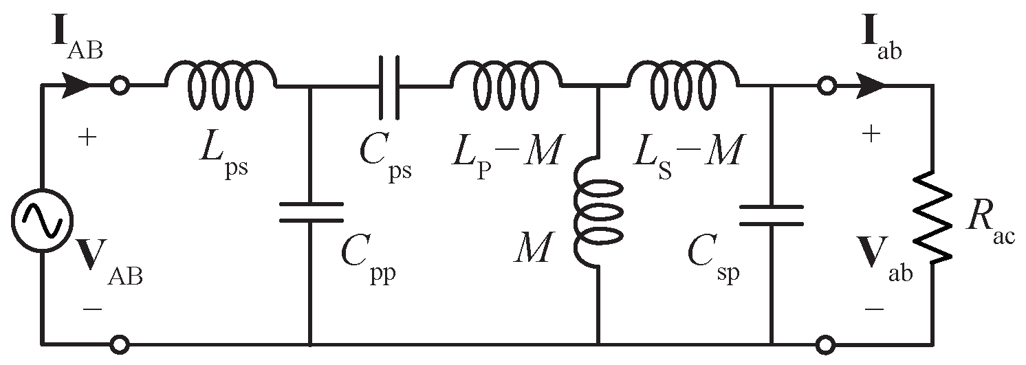
Figure 2 shows an LCC-parallel compensated IPT system. It consists of a single phase full-bridge inverter, primary and secondary side compensation networks, a loosely coupled transformer, a rectifier with an L C filter, and the load. L ps , C pp and C ps represent the series compensation inductor, parallel compensation capacitor and series compensation capacitor in the primary side, respectively, which form the primary compensation circuit. C sp is the secondary parallel compensation capacitor. L P and L S represent the primary and secondary self-inductances, and M is the mutual inductance. V AB and I AB are the phasor forms of the input voltage and current of the LCC-parallel compensation topology, and V ab and I ab are the output variables. In this paper, a frequency-domain equivalent circuit is adopted and only the fundamental component is considered for simplicity. It means the first-order RMS value of the output voltage of the inverter and equivalent AC resistance for the rectifier with an L C filter are expressed as V AB = 2 2 V dc 2 2 V dc π π and R ac = π 2 R L π 2 R L 8 8 [25] respectively. Moreover, the loosely coupled transformer is equivalent to its T-mode [26]. Then the LCC-parallel compensated IPT system is modeled as Figure 3.

2.2. CV Charging Mode at a Zero Phase Angle Frequency

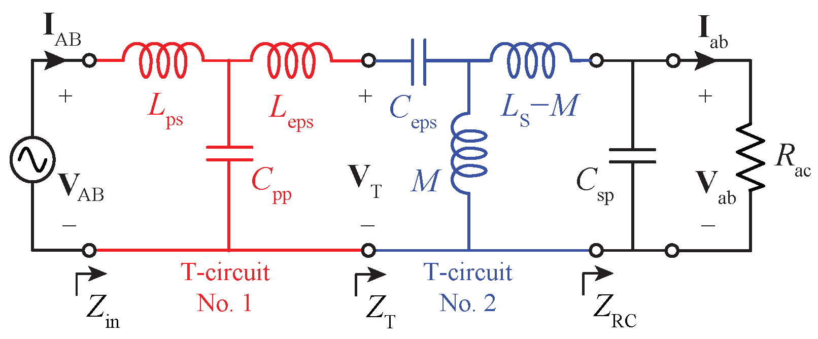
An arbitrary higher-order resonant network can be modeled as multistage T-circuit in series to analyze its load-independent voltage transfer characteristic [11]. For Figure 3, it can be equivalent to Figure 4. Specifically, the series-connected branch of C ps and ( L P M ) is equivalent to L eps and C eps . The equivalent variables can be expressed as,
1 j ω C ps + j ω L P M = j ω L eps + 1 j ω C eps
where, ω represents the resonant frequency of the LCC-parallel compensation topology.
As shown in Figure 4, one just need to analyze the voltage transfer characteristics of the two-stage T-circuit, then to investigate the load-independent CV mode of the LCC-parallel compensated IPT system. According to the analysis of the T-circuit in [11], when the following resonant methods for Figure 4 are designed:
ω 2 = L ps + L eps L ps L eps C pp = M + L S M M L S M C eps
The output voltage (or the voltage transfer ratio, which is the ratio of the output voltage to the input voltage) of the LCC-parallel resonant tank network is derived as
V ab = M + L S M M V T = L S M L eps L ps V AB
G vv = V ab V AB = L S M L eps L ps
It can be seen that G vv is independent of the load. It means that the load-independent CV output can be achieved when the LCC-parallel resonant tank network is driven by a constant voltage source and resonates at the condition of (2).
Then, the input impedance Z in of Figure 4 is expressed as
Z in = R ac 1 j ω C sp + j ω L S M j ω M + 1 j ω C eps + j ω L eps 1 j ω C pp + j ω L ps
Under the resonant conditions of (2), Z in can be simplified as
Z in = Re Z in + j · Im Z in = Z T 1 j ω C pp + j ω L ps Z T + j ω L eps + 1 j ω C pp
where
Z T = Z RC j ω M + 1 j ω C eps Z RC + j ω L S M + j ω M
Z RC = R ac 1 j ω C sp R ac + 1 j ω C sp
To achieve unit power factor, namely zero phase angle, the imaginary part of Z in , Im Z in , should be designed to be zero. From (5), the resonant condition for achieving Im Z in = 0 is given by
L S M L ps M C eps + L S 2 L eps C sp = M 2 + L S L eps L ps C pp
In this case, the purely resistive input impedance is achieved and expressed as
R in = Re Z in = R ac L ps 2 M 2 L eps 2 L S 2 = R ac G AB 2
So, the load-independent CV output with ZPA condition is realized for the LCC-parallel resonant tank network under the conditions of (2) and (7).

3. Efficiency Optimization

When the compensation components and the primary and secondary coils have parasitic resistances, the LCC-parallel compensation topology is shown in Figure 5. R Lps , R Cpp , R Cps , R Lp , R m , R Ls , and R Csp represent the equivalent series resistances (ESRs) of the corresponding passive components. The parasitic resistance of the inductor is calculated by ω L ω L Q Q (Q represents the quality factor of the inductor), and that of the capacitor is expressed by tan δ tan δ ( ω C ) ( ω C ) ( tan δ is the dissipation factor of the capacitor).
The input impedance of Figure 5 is given by
Z in = R ac Z Csp + Z Ls Z m + Z Lp + Z Cps Z Cpp + Z Lps
where,
Z Csp = R Csp + 1 j ω C sp , Z Ls = R Ls + j ω L S M
Z m = R m + j ω M , Z Lp = R Lp + j ω L P M
Z Cps = R Cps + 1 j ω C ps , Z Cpp = R Cpp + 1 j ω C pp
Z Lps = R Lps + j ω L ps
According to (9), the currents flowing through L ps , C pp , C ps , M and C sp ( I AB , I Cpp , I Lp , I Lm , and I Csp ) and the output current I ab are expressed by the following equations, respectively,
I AB = V AB Z in
I Cpp = V AB I AB Z Lps Z Cpp
I Lp = I AB I Cpp
I Lm = V AB I AB Z Lps I Lp Z Cps + Z Lp Z m
I Ls = I Lp I Lm
I Csp = V AB I AB Z Lps I Lp Z Cps + Z Lp I Ls Z Ls Z Csp
I ab = I Ls I Csp
Then, the voltage transfer ratio of the LCC-parallel compensation topology with resonant tank losses included is expressed as,
G vv = V ab V AB = I ab R ac V AB
The output power of the LCC-parallel resonant tank network is derived as P out = I ab 2 R ac , then its transfer efficiency is given by (13).
η = P out P out + P loss = I ab 2 R ac I ab 2 R ac + I Csp 2 R Csp + I Ls 2 R Ls + I Lm 2 R m + I Lp 2 R Lp + R Cps + I Cpp 2 R Cpp + I AB 2 R Lps
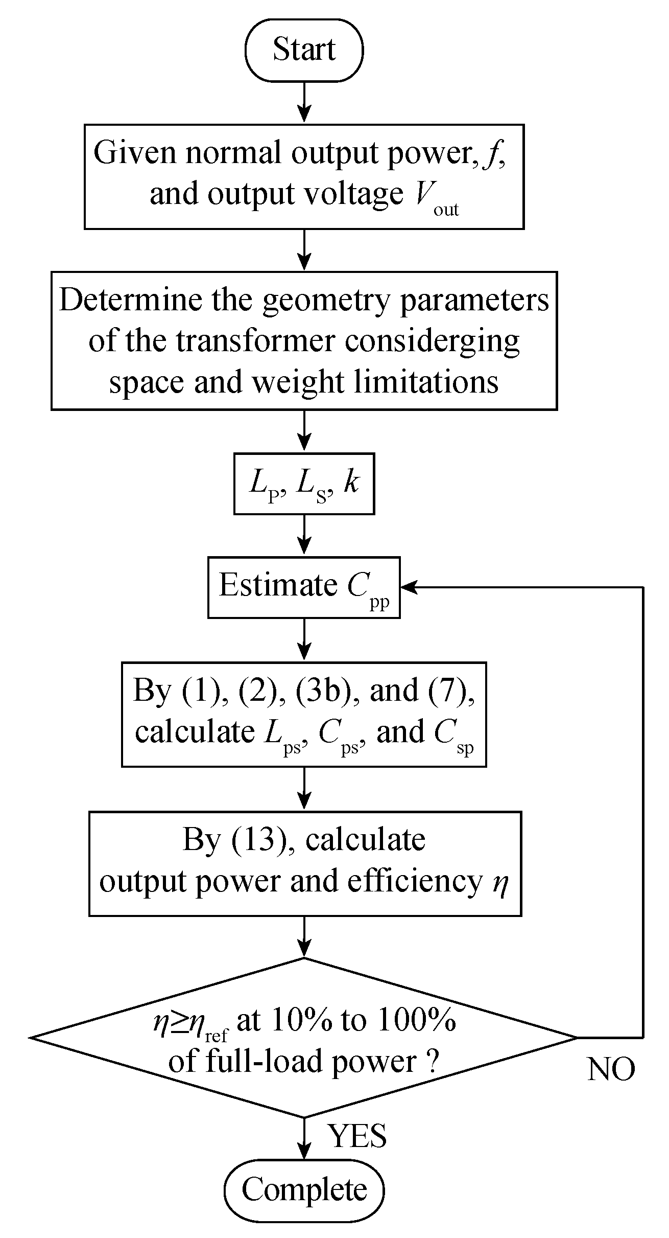
Figure 6 shows the proposed flow chart of the efficiency optimization for the LCC-parallel compensation topology. The detailed design procedure is summarized as follows:
  • Determine the power level, operating frequency f, and nominal output charging voltage V o ;
  • The geometry parameters of the primary and secondary coils, for example the outer diameter and coils category, should then be determined according to the power level, as well as the space and weight constrained. Followed by designing the self-inductances of the primary and secondary coils and the coupling coefficient;
  • Estimate the parallel compensation capacitor at the primary side C pp ;
  • Calculate L ps , C ps , and C sp by (1), (2), (3b) and (7)
  • Calculate the output power and efficiency by (13), until finding out the efficiency equalization point over the full range of CV charging profile;
  • Finally, build the experimental prototype based on the designed parameters.
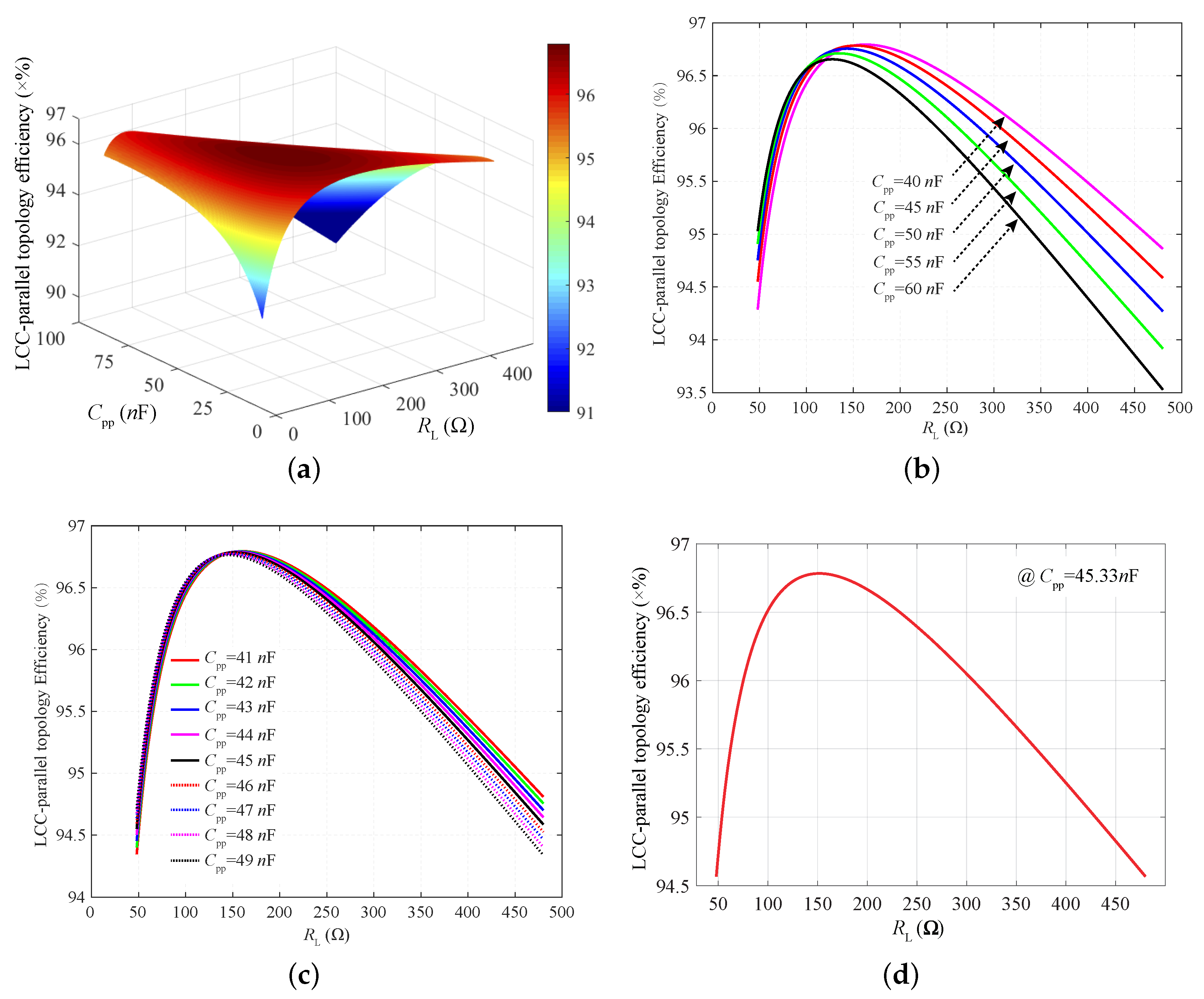
An IPT battery charging system with 1A charging current and 48 V charging voltage is analyzed and designed in this paper. The operating frequency is set to 200 kHz, which is in compliance with Qi standard [27]. According to Figure 6, the efficiency of the LCC-parallel resonant tank circuit with losses included is shown in Figure 7a–c. Finally, when C pp is set to 45.33 nF, the optimized efficiency is shown in Figure 7d. It can be seen that the efficiency of greater than 94.5% is achieved from 48 Ω (full-load power) to 480 Ω . Based on the optimized C pp , the designed system parameters are tabulated in Table 1.
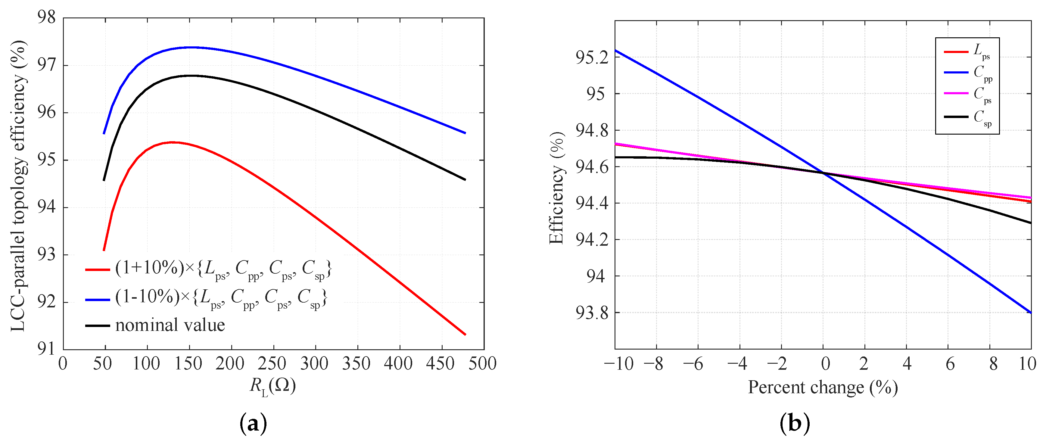
Figure 8a presents the effect of the parameter variation on the system efficiency. The worst case (lowest efficiency) happens when all the parameter values are +10% away from the nominal value. In addition, a higher efficiency can be achieved when the values of all the compensation components are changed by −10%. In this case, however, the load-independent CV output characteristic and ZPA operating condition cannot be maintained. Figure 8b shows the simulated efficiency in respect to the variations of all compensation components. It can be seen that the efficiency is the least sensitive to the variation of C ps . C pp has the significant effect on the efficiency. It means C pp should be designed carefully before actual physical implementation.

4. Evaluations

4.1. Simulation and Experimental Results

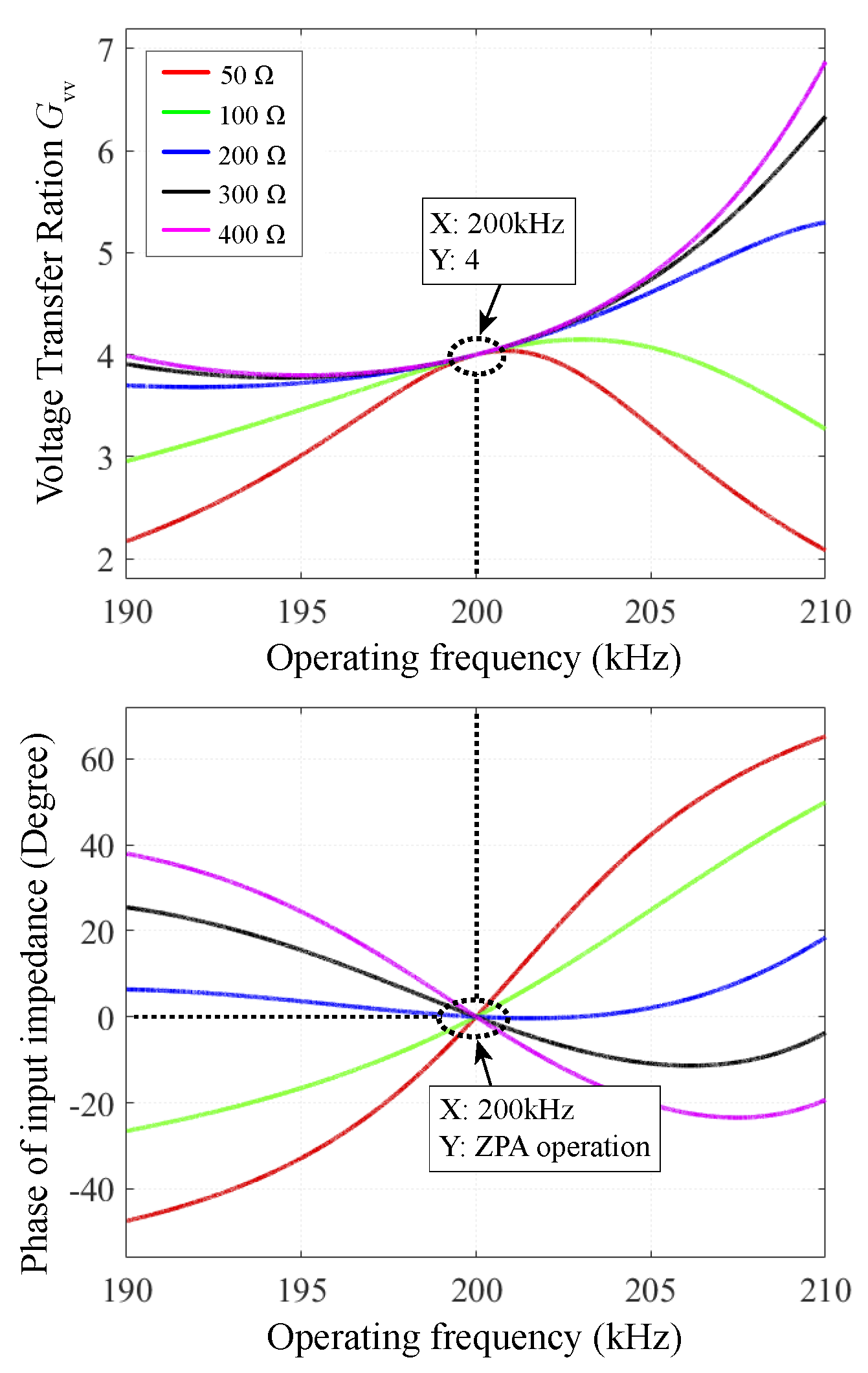
Figure 9 shows the simulated voltage transfer ratio and phase of the input impedance of the LCC-parallel resonant tank network without considering the power losses. It can be seen that the constant voltage transfer ratio and ZPA condition were achieved at 200 kHz, which verifies the theoretic analysis in Section 2 and the designed parameters shown in Table 1.
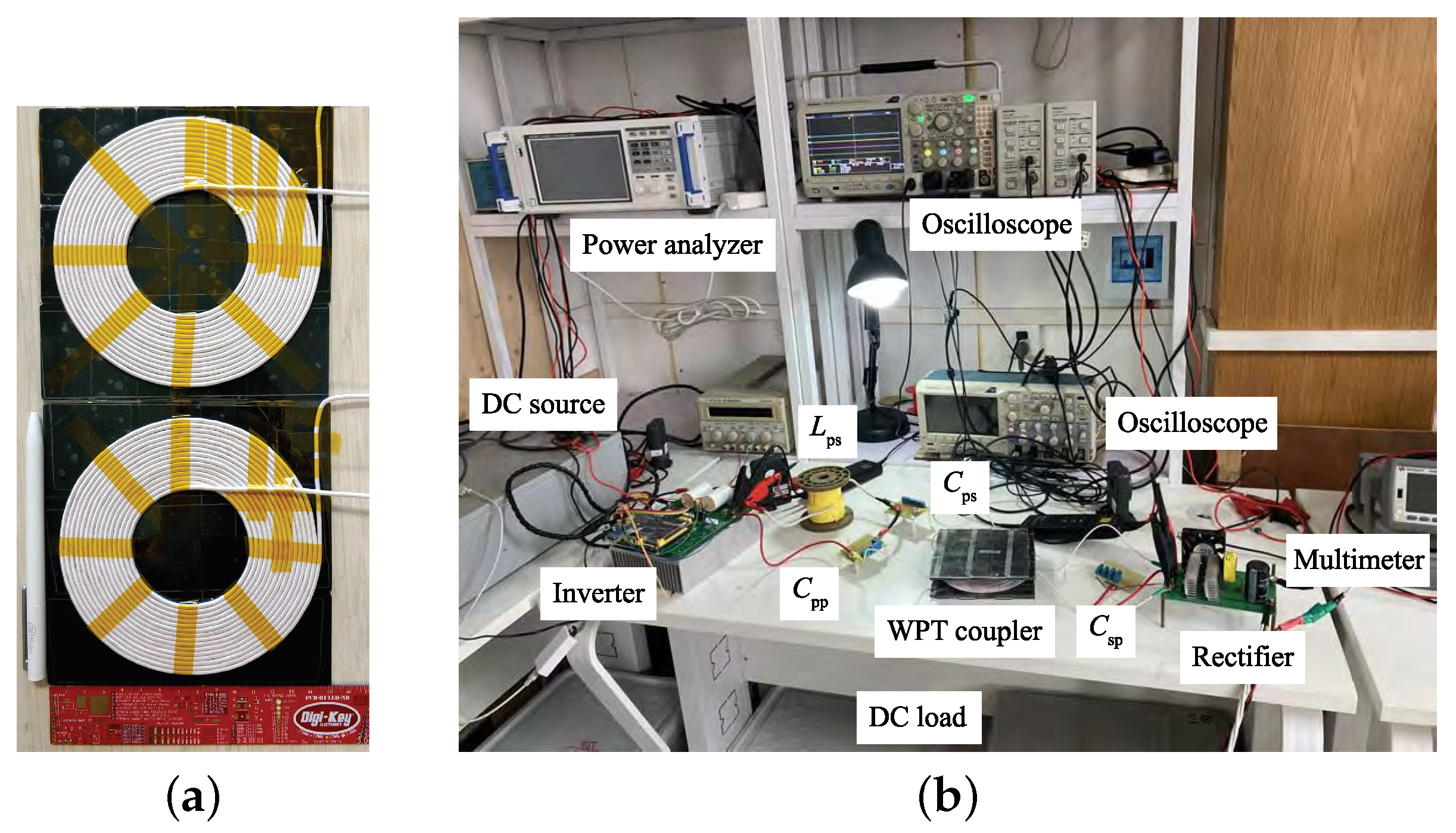
To verify the proposed efficiency optimization method, an LCC-parallel compensated IPT prototype was implemented. The symmetrical unipolar coils with the shape of circle were used for both primary and secondary sides, which are shown in Figure 10a.
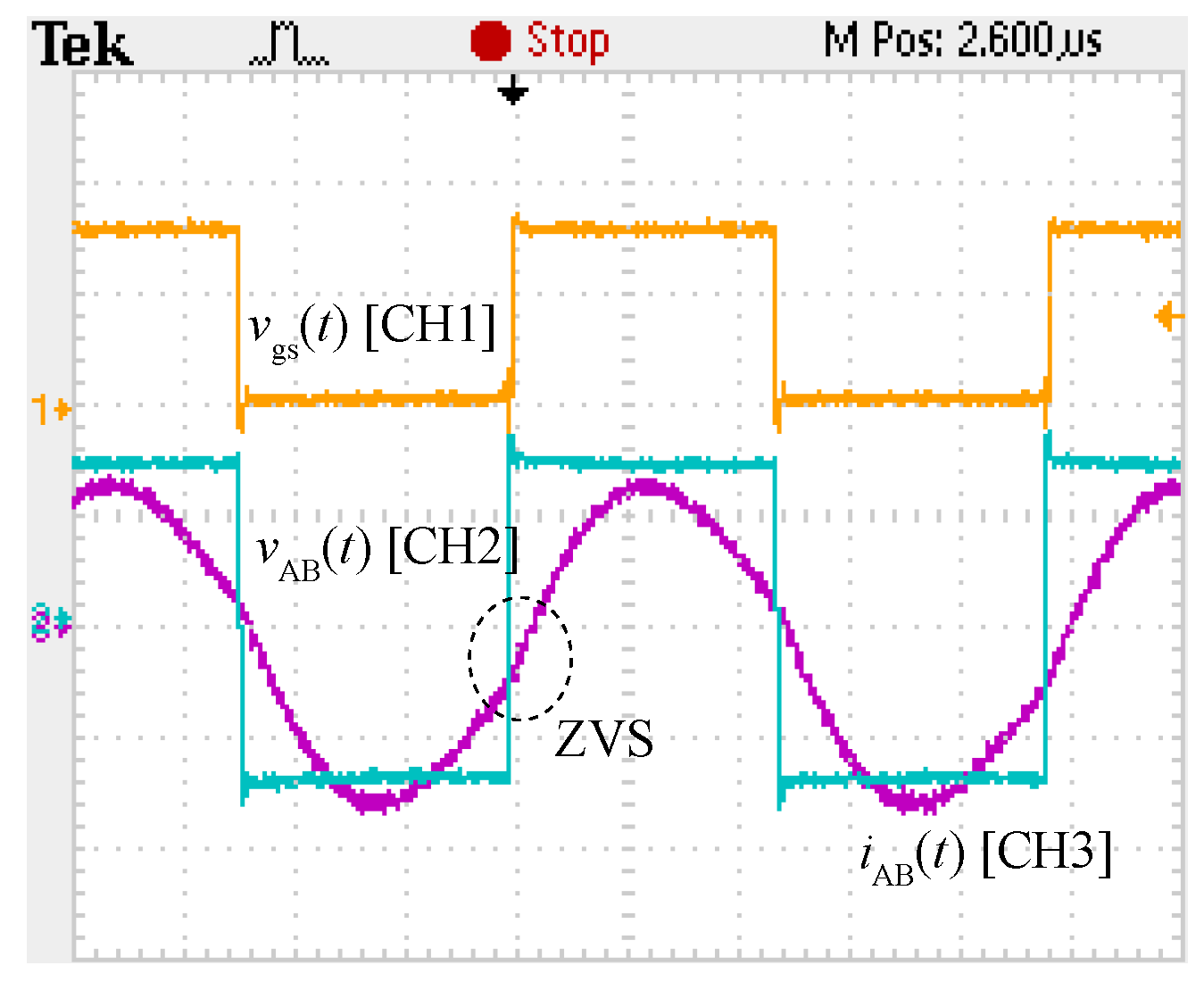
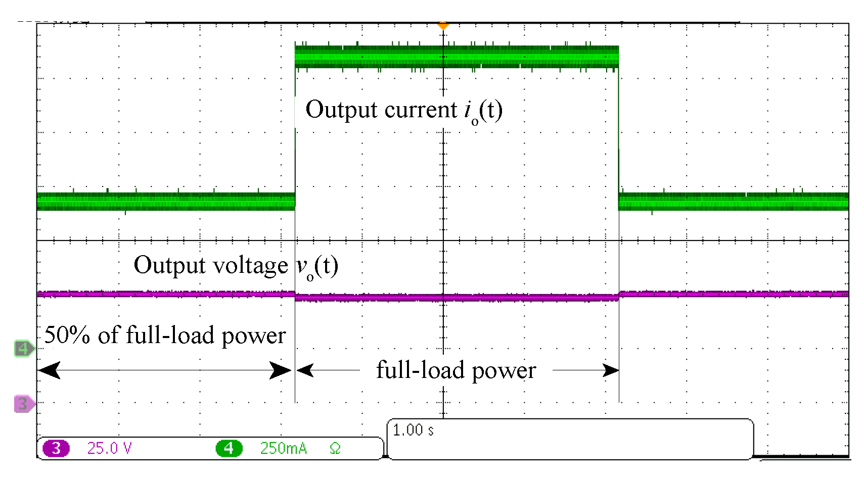
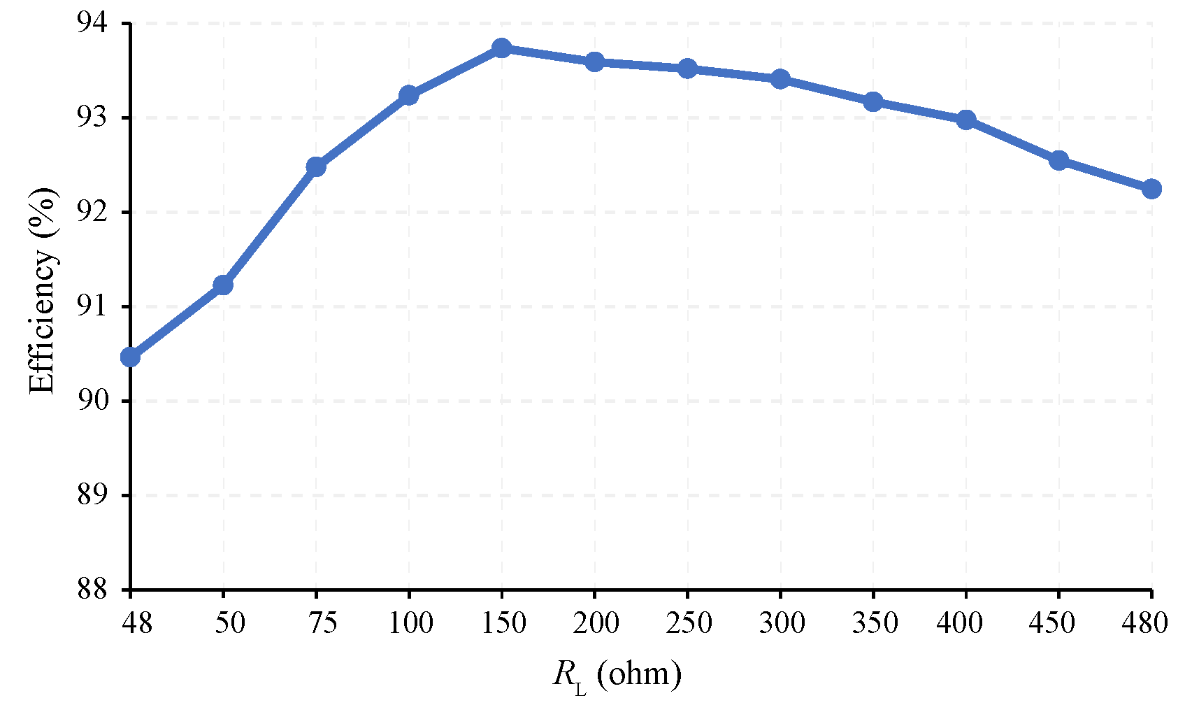
Figure 11 shows the output voltage v AB ( t ) and current i AB ( t ) of the inverter. It can be seen that i AB ( t ) slightly lagged v AB ( t ) , which means ZVS was achieved for the MOSFET-based inverter. Figure 12 shows the transient waveforms of the system output current and voltage. At different load conditions, the constant output voltage was obtained. The measured system efficiency is shown in Figure 13. The DC–DC transfer efficiency of greater than 90% was achieved during the whole CV charging profile.
The performances of the proposed IPT system in this paper were compared with the previous works, as given in Table 2. The designed IPT system could achieve competitive efficiency over the full range of CV charging mode without the help of extra DC–DC converter or complex control method.

4.2. Discussion

4.2.1. CC/CV Charging Mode with a Hybrid Topology

A PP (parallel–parallel) compensation topology with a series compensation inductor in primary side can achieve load-independent CC output at a load-independent ZPA frequency [13]. So, a hybrid topology shown in Figure 14 can be designed to achieve a CC/CV charging profile. For Figure 14, when the switch S 5 is on, it is PP compensation topology with inductor L ps . The switch should be high-frequency single-pole single-throw AC switch, which can be implemented with power relay or power semiconductor device, for example, two anti-series MOSFETs or two anti-parallel IGBTs. On the other hand, when S 5 is off, the system is changed to LCC-parallel topology. In this case, CC and CV output characteristics both with the ZPA condition can be achieved. The light-load efficiency in CV mode can be improved according to the analysis in the previous section.

4.2.2. CC/CV Charging Mode at Two Different Frequencies

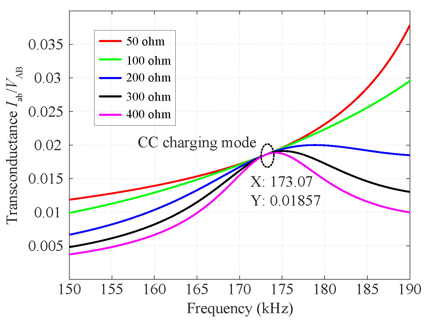
Figure 15 shows the transconductance (the ratio of the output current to the input voltage) of the LCC-parallel compensation topology. It can be seen that load-independent transconductance is achieved at 173.07 kHz. So, the CC output characteristic can be implemented when the system operates at 173.07 kHz. Subsequently, when the operating frequency is changed to 200 kHz, CV output is obtained. In this case, a variable frequency control method can also be used to achieve CC/CV charging profile with high efficiency for battery charging application.

5. Conclusions

This paper firstly analyzes the equivalent circuit and resonant conditions of the LCC-parallel compensation topology in inductive battery charging system to achieve load-independent CV output at a ZPA frequency. In CV charging mode, a light-load efficiency optimization method is proposed. An LCC-parallel compensated IPT prototype is implemented to verify the theoretical analysis. Over the full range of CV charging mode, a DC-to-DC transfer efficiency of greater than 90.48% is achieved. The designed LCC-parallel compensation network can be applied to a hybrid IPT topology and operates in CV mode to improve the system efficiency.

Author Contributions

S.Y. performed all calculations, simulations and original draft preparation. All authors contributed to interpretation of results, and to editing into the final manuscript. All authors have read and agreed to the published version of the manuscript.

Funding

This research received no external funding.

Acknowledgments

The authors would like to thank the anonymous reviewers for their constructive comments.

Conflicts of Interest

The authors declare no conflict of interest.

References

  1. Li, S.; Mi, C.C. Wireless Power Transfer for Electric Vehicle Applications. IEEE J. Emerg. Sel. Top. Power Electron. 2015, 3, 4–17. [Google Scholar]
  2. Zhang, Z.; Pang, H.; Georgiadis, A.; Cecati, C. Wireless Power Transfer Overview. IEEE Trans. Ind. Electron. 2019, 66, 1044–1058. [Google Scholar] [CrossRef]
  3. Buja, G.; Bertoluzzo, M.; Mude, K.N. Design and Experimentation of WPT Charger for Electric City Car. IEEE Trans. Ind. Electron. 2015, 62, 7436–7447. [Google Scholar] [CrossRef]
  4. Vu, V.-B.; Tran, D.-H.; Choi, W. Implementation of the Constant Current and Constant Voltage Charge of Inductive Power Transfer Systems With the Double-Sided LCC Compensation Topology for Electric Vehicle Battery Charge Applications. IEEE Trans. Power Electron. 2018, 33, 7398–7410. [Google Scholar] [CrossRef] [Green Version]
  5. Qu, X.; Chu, H.; Wong, S.C.; Tse, C.K. An IPT Battery Charger with Near Unity Power Factor and Load-independent Constant Output Combating Design Constraints of Input Voltage and Transformer Parameters. IEEE Trans. Power Electron. 2018, 34, 7719–7727. [Google Scholar] [CrossRef]
  6. Zheng, C.; Lai, J.S.; Chen, R.; Faraci, W.E.; Zahid, Z.U.; Gu, B.; Zhang, L.; Lisi, G.; Anderson, D. High-Efficiency Contactless Power Transfer System for Electric Vehicle Battery Charging Application (Variable frequency). IEEE J. Emerg. Sel. Top. Power Electron. 2015, 3, 65–74. [Google Scholar] [CrossRef]
  7. Wu, H.H.; Gilchrist, A.; Sealy, K.D.; Bronson, D. A High Efficiency 5 kW Inductive Charger for EVs Using Dual Side Control. IEEE Trans. Ind. Inform. 2012, 8, 585–595. [Google Scholar] [CrossRef] [Green Version]
  8. Kim, M.; Joo, D.M.; Lee, B.K. Design and Control of Inductive Power Transfer System for Electric Vehicles Considering Wide Variation of Output Voltage and Coupling Coefficient. IEEE Trans. Power Electron. 2019, 34, 1197–1208. [Google Scholar] [CrossRef]
  9. Li, S.; Li, W.; Deng, J.; Nguyen, T.D.; Mi, C.C. A Double-Sided LCC Compensation Network and Its Tuning Method for Wireless Power Transfer. IEEE Trans. Veh. Technol. 2015, 64, 2261–2273. [Google Scholar] [CrossRef]
  10. Zhang, W.; Mi, C.C. Compensation Topologies of High-Power Wireless Power Transfer Systems. IEEE Trans. Veh. Technol. 2016, 65, 4768–4778. [Google Scholar] [CrossRef]
  11. Lu, J.; Zhu, G.; Lin, D.; Wong, S.-C.; Jiang, J. Load-Independent Voltage and Current Transfer Characteristics of High-Order Resonant Network in IPT System. IEEE J. Emerg. Sel. Top. Power Electron. 2018, 7, 422–436. [Google Scholar] [CrossRef]
  12. Zhang, W.; Wong, S.C.; Tse, C.K.; Cheng, Q. Load-Independent Duality of Current and Voltage Outputs of a Series- or Parallel-Compensated Inductive Power Transfer Converter With Optimized Efficiency. IEEE J. Emerg. Sel. Top. Power Electron. 2015, 3, 137–146. [Google Scholar] [CrossRef]
  13. Qu, X.; Han, H.; Wong, S.C.; Tse, C.K.; Chen, W. Hybrid IPT Topologies With Constant Current or Constant Voltage Output for Battery Charging Applications. IEEE Trans. Power Electron. 2015, 30, 6329–6337. [Google Scholar] [CrossRef]
  14. Qu, X.; Jing, Y.; Han, H.; Wong, S.C.; Tse, C.K. Higher Order Compensation for Inductive-Power-Transfer Converters with Constant-Voltage or Constant-Current Output Combating Transformer Parameter Constraints. IEEE Trans. Power Electron. 2017, 32, 394–405. [Google Scholar] [CrossRef]
  15. Hou, J.; Chen, Q.; Zhang, Z.; Wong, S.-C.; Tse, C.K. Analysis of Output Current Characteristics for Higher Order Primary Compensation in Inductive Power Transfer Systems. IEEE Trans. Power Electron. 2018, 33, 6807–6821. [Google Scholar] [CrossRef]
  16. Hou, J.; Chen, Q.; Zhang, Z.; Wong, S.-C.; Tse, C.K.; Ruan, X. Analysis and Control of Series/Series-Parallel Compensated Resonant Converter for Contactless Power Transfer. IEEE J. Emerg. Sel. Top. Power Electron. 2015, 3, 124–136. [Google Scholar]
  17. Wang, Y.; Shi, G.; Yao, Y.; Alonso, J.M.; Guo, W.; Liu, X.; Xu, D. A Double-T-Type Compensation Network and Its Tuning Method for IPT System. IEEE Trans. Ind. Appl. 2017, 53, 4757–47675. [Google Scholar] [CrossRef]
  18. Chen, Y.; Yang, B.; Kou, Z.; He, Z.; Cao, G.; Mai, R. Hybrid and Reconfigurable IPT Systems with High-Misalignment Tolerance for Constant-Current and Constant-Voltage Battery Charging. IEEE Trans. Power Electron. 2018, 33, 8259–8269. [Google Scholar] [CrossRef]
  19. Lu, J.; Zhu, G.; Li, W.; Li, B. Load-Independent ZPA Conditions in Both Constant Current and Constant Voltage Modes of LCC-Series Compensated IPT System. In Proceedings of the IEEE Wireless Power Transfer Conference (WPTC), Montreal, QC, Canada, 3–7 June 2018. [Google Scholar]
  20. Zhong, W.; Hui, S.Y.R. Maximum Energy Efficiency Tracking for Wireless Power Transfer Systems. IEEE Trans. Power Electron. 2015, 30, 4025–4034. [Google Scholar] [CrossRef] [Green Version]
  21. Li, H.; Li, J.; Wang, K.; Chen, W.; Yang, X. A Maximum Efficiency Point Tracking Control Scheme for Wireless Power Transfer Systems Using Magnetic Resonant Coupling. IEEE Trans. Power Electron. 2015, 30, 3998–4008. [Google Scholar] [CrossRef]
  22. Huang, Z.; Wong, S.C.; Tse, C.K. Control Design for Optimizing Efficiency in Inductive Power Transfer Systems. IEEE Trans. Power Electron. 2018, 33, 4523–4534. [Google Scholar] [CrossRef]
  23. Mai, R.; Liu, Y.; Li, Y.; Yue, P.; Cao, G.; He, Z. An Active-Rectifier-Based Maximum Efficiency Tracking Method Using an Additional Measurement Coil for Wireless Power Transfer. IEEE Trans. Power Electron. 2018, 33, 716–728. [Google Scholar] [CrossRef]
  24. Huang, Z.; Wong, S.C.; Tse, C.K. An Inductive Power Transfer Converter with High Efficiency throughout Battery Charging Process. IEEE Trans. Power Electron. 2019, 34, 10245–10255. [Google Scholar] [CrossRef]
  25. Steigerwald, R.L. A comparison of half-bridge resonant converter topologies. IEEE Trans. Power Electron. 1988, 3, 174–182. [Google Scholar] [CrossRef]
  26. Sohn, Y.-H.; Choi, B.; Cho, G.-H.; Rim, C. Gyrator-Based Analysis of Resonant Circuits in Inductive Power Transfer Systems. IEEE Trans. Power Electron. 2015, 31, 6824–6843. [Google Scholar] [CrossRef]
  27. The Qi Wireless Power Transfer System Power Class 0 Specification: Reference Designs; Parts 1 and 2; Wireless Power Consortium: Piscataway, NJ, USA, 2017.
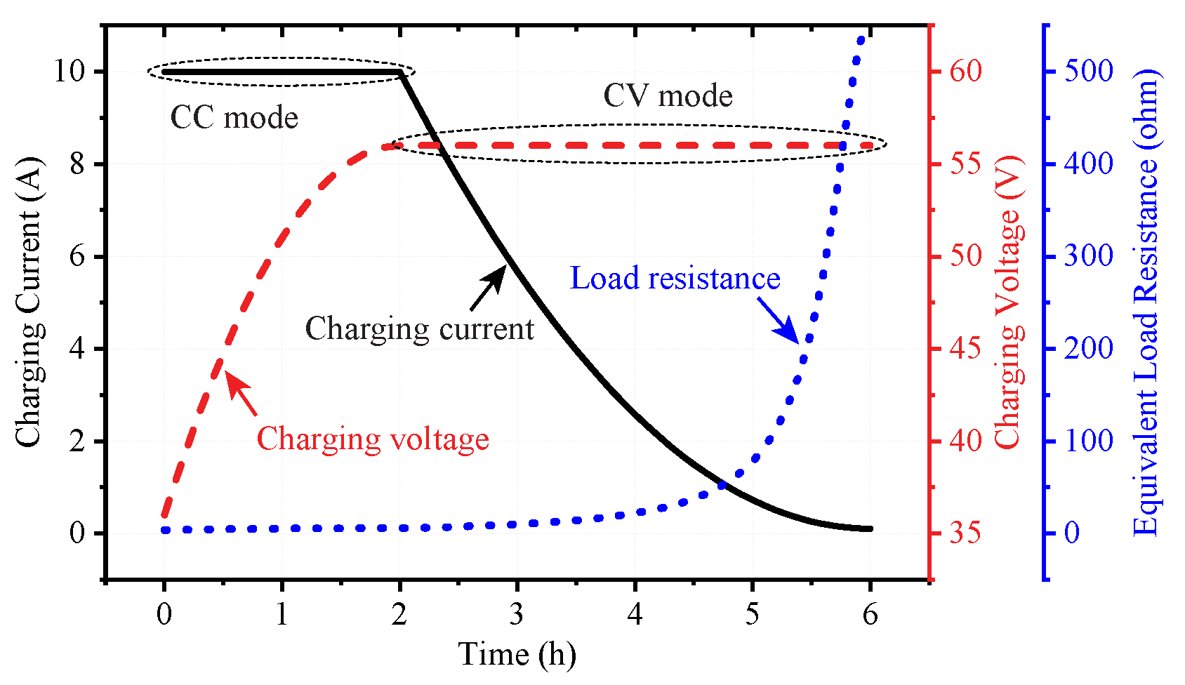
Figure 1. A classical constant current/constant voltage (CC/CV)-based charging process [3].
Electronics 09 02080 g001
Figure 2. An LCC-parallel compensated inductive power transfer (IPT) system.
Electronics 09 02080 g002
Figure 3. The LCC-parallel resonant tank network.
Electronics 09 02080 g003
Figure 4. Equivalent circuit of Figure 3 for achieving constant voltage output.
Electronics 09 02080 g004
Figure 5. Equivalent circuit of the LCC-parallel compensation topology with resonant circuit losses included.
Electronics 09 02080 g005
Figure 6. Design chart of the compensation components of the LCC-parallel topology.
Electronics 09 02080 g006
Figure 7. (ac) Optimized efficiency of the LCC-parallel compensation topology ( η ) versus R L and C pp and (d) η with respect to R L when C pp is set to 45.33 nF.
Electronics 09 02080 g007
Figure 8. (a) Effect of the parameter variation from the nominal value on the system efficiency and (b) system efficiency in respect to the percent changes of all compensation components.
Electronics 09 02080 g008
Figure 9. Voltage transfer ratio and input phase angle of the LCC-parallel compensation topology versus the frequency for different load conditions.
Electronics 09 02080 g009
Figure 10. (a) The designed IPT coupler and (b) experimental setup.
Electronics 09 02080 g010
Figure 11. Experimental waveforms of v AB ( t ) and i AB ( t ) .
Electronics 09 02080 g011
Figure 12. Transient waveforms of the output current i o ( t ) and voltage v o ( t ) .
Electronics 09 02080 g012
Figure 13. System efficiency.
Electronics 09 02080 g013
Figure 14. A hybrid IPT topology.
Electronics 09 02080 g014
Figure 15. Simulated transconductance of the LCC-parallel compensation topology.
Electronics 09 02080 g015
Table 1. System parameters of the LCC-parallel compensated IPT converter.
ParameterSymbolCalculated ValueMeasured Value
Primary self-inductance L p 40 μ H39.65 μ H
Secondary self-inductance L s 40 μ H41.02 μ H
Coupling coefficientk0.30.289
Operation frequencyf200 kHz-
Nominal output voltage V o 48 V-
Nominal output current I o 1 A-
Minimum output current I o , min 0.1 A-
Equivalent load resistance R L 48–480 Ω -
Voltage transfer ratio G vv 4-
Primary compensation inductor L ps 25.612 μ H25.44 μ H
Primary parallel compensation capacitor C pp 45.33 nF45.21 nF
Primary series compensation capacitor C ps 111.76 nF110.86 nF
Secondary parallel compensation capacitor C sp 19.231 nF19.94 nF
Table 2. Comparison of the publications for light-load efficiency optimization.
Referencef (kHz) P out V o η (%)DesignLimitation
This paper20048 W48 V≥90.48--
[20]1002.5 W2.5 V≤69Minimum input current trackingExtra DC–DC converter
[21]515100 W100 V79Maximum efficiency tracking
[22]20060 W30 V≤90Voltage ratio control
[23]30800 W120 V91.7 Active rectifier
[24]49.98156 W52 V≤90
Publisher’s Note: MDPI stays neutral with regard to jurisdictional claims in published maps and institutional affiliations.