Article

Reverse Conduction Loss Minimization in GaN‑Based PMSM Drive

Department of Electrical Drives and Traction, Faculty of Electrical Engineering, Czech Technical University in Prague, 16627 Prague, Czech Republic
*
Author to whom correspondence should be addressed.
Electronics 2020, 9(11), 1973; https://doi.org/10.3390/electronics9111973
Submission received: 24 October 2020 / Revised: 17 November 2020 / Accepted: 20 November 2020 / Published: 22 November 2020
(This article belongs to the Section Power Electronics)

Abstract

:
Gallium nitride (GaN) devices are becoming more popular in power semiconductor converters. Due to the absence of the freewheeling substrate diode, the reverse conduction region is used in GaN transistors to conduct the freewheeling current. However, the voltage drop across the device in the reverse conduction mode is relatively high, causing additional power losses. These losses can be optimized by adequately adjusting the dead-time issued by the microcontroller. The dead-time loss minimization strategies presented in the literature have the common disadvantage that either additional hardware or specific converter data are needed for their proper operation. Therefore, this paper’s motivation is to present a novel dead-time loss minimization method for GaN-based high-frequency switching converters for electric drives that does not impose additional requirements on the hardware design phase and converter data acquisition. The method is based on optimizing the current controllers’ output with a simple perturb-and-observe tracker. The experimental results show that the proposed approach can minimize the dead-time losses over the whole drive’s operating range at the cost of only a moderate increase in software complexity.

1. Introduction

Within electrical drives, especially when powered by batteries, efficiency and power density are essential aspects. The design of small and highly efficient power converters for electric motor control demands wide bandgap semiconductors such as those based on silicon carbide (SiC) and gallium nitride (GaN). These materials, with a high inner electric field, improve the transistor’s parameters, such as the current density and on-state resistance. Furthermore, the low parasitic capacitances allow them to operate at higher switching frequencies than silicon devices [1,2,3,4]. Besides, GaN-based transistors have no reverse recovery charge due to the absence of the freewheeling diode. However, fast-switching devices also bring challenges to the circuit board design and control strategies [5].
With the absence of the freewheeling diode, the reverse conduction region is used to conduct the current [6]. However, a significant voltage drop in the reverse conduction mode exists, consisting of a gate threshold and turn-off voltage, which means the load current should be immediately transferred to the complementary switch in the half-bridge to avoid additional losses. In other words, the delay between when one transistor is turned off and the other is turned on, which is called the dead-time, needs to be set precisely [7]. However, the optimum dead-time for GaN transistors changes with the converter output power and input DC-link voltage [8]. An in-depth investigation in [9] shows the need to modify both the rising and falling edges of the microcontroller (MCU) control signal with the variable dead-time.
There are multiple approaches to proper dead-time selection. One option is to manually create a look-up table for a specific converter so the controller can set the dead-time accordingly [10]. The half-bridge configuration can also be equipped with a special sampling circuit to measure the actual time delay between the upper and lower transistors’ switching instants [11,12]. The model-based methods presented in [13,14] calculate the optimum dead-time depending on the converter’s operating point reconstructed from the measured values. Furthermore, maximum efficiency point tracking algorithms can be used within various types of converters for dead-time optimization in the case of a variable switching frequency [15]. GaN drivers with built-in dead-time minimization circuits are being developed too; however, their operation is limited to the type of converter they are specifically designed for, such as highly efficient miniature DC/DC converters [16].
In this paper, an online method of dead-time loss minimization for a vector-controlled permanent magnet synchronous motor (PMSM) supplied by a three-phase voltage-source inverter (VSI) controlled by a space-vector modulation (SVM) is proposed. The method is intended to improve and extend the authors’ work presented in [17], where a similar approach was discussed for a half-bridge DC/DC converter topology. The method’s principle is based on an online analysis of the current controllers’ output at multiple operating points. Its main advantage is that no prior converter data and additional hardware are needed. The method, along with the motor control algorithm, was programmed into an MCU and verified experimentally. Measured data at multiple operating points are presented at the end of the paper.

2. Theoretical Analysis

Since the three-phase two-level VSI consists of three half-bridges connected in parallel, the dead-time theoretical analysis was conducted on a single half-bridge. The typical GaN-based half-bridge configuration is shown in Figure 1. The actual transistors’ switching depends not only on the dead-time issued by the MCU but also on the propagation delay introduced by the driver, the delay caused by a digital isolator (when used for the high-side switch), and the delay given by the transistors’ intrinsic properties. Compared to silicon devices, in the case of fast-switching GaN transistors, the driver’s delay is comparable to the transistor’s delay [16]. Furthermore, the driver’s delay varies with the temperature and supply voltage, and the transistors’ delay, with the DC-link voltage and the load current. In the following text, the actual time duration when both transistors in the half-bridge are in the “off” state will be referred to as the “output dead-time”. Similarly, the converter’s output voltage actual transition will be referred to as the “output duty cycle”.

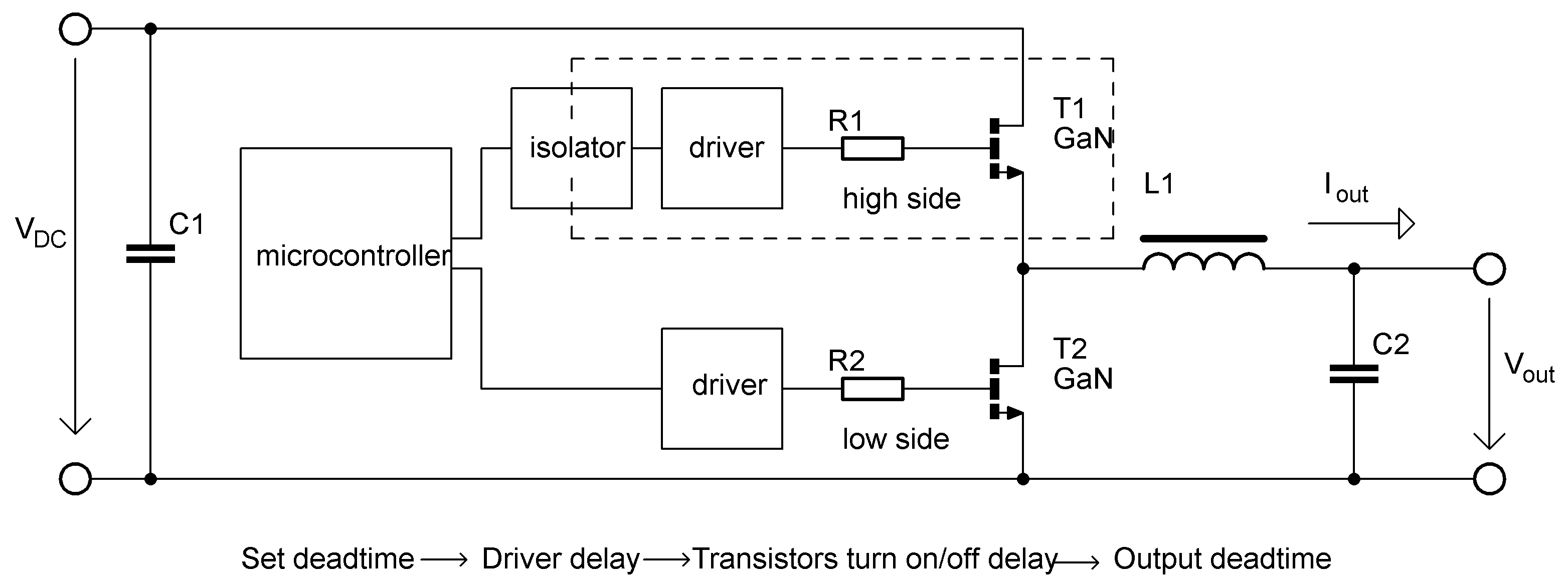
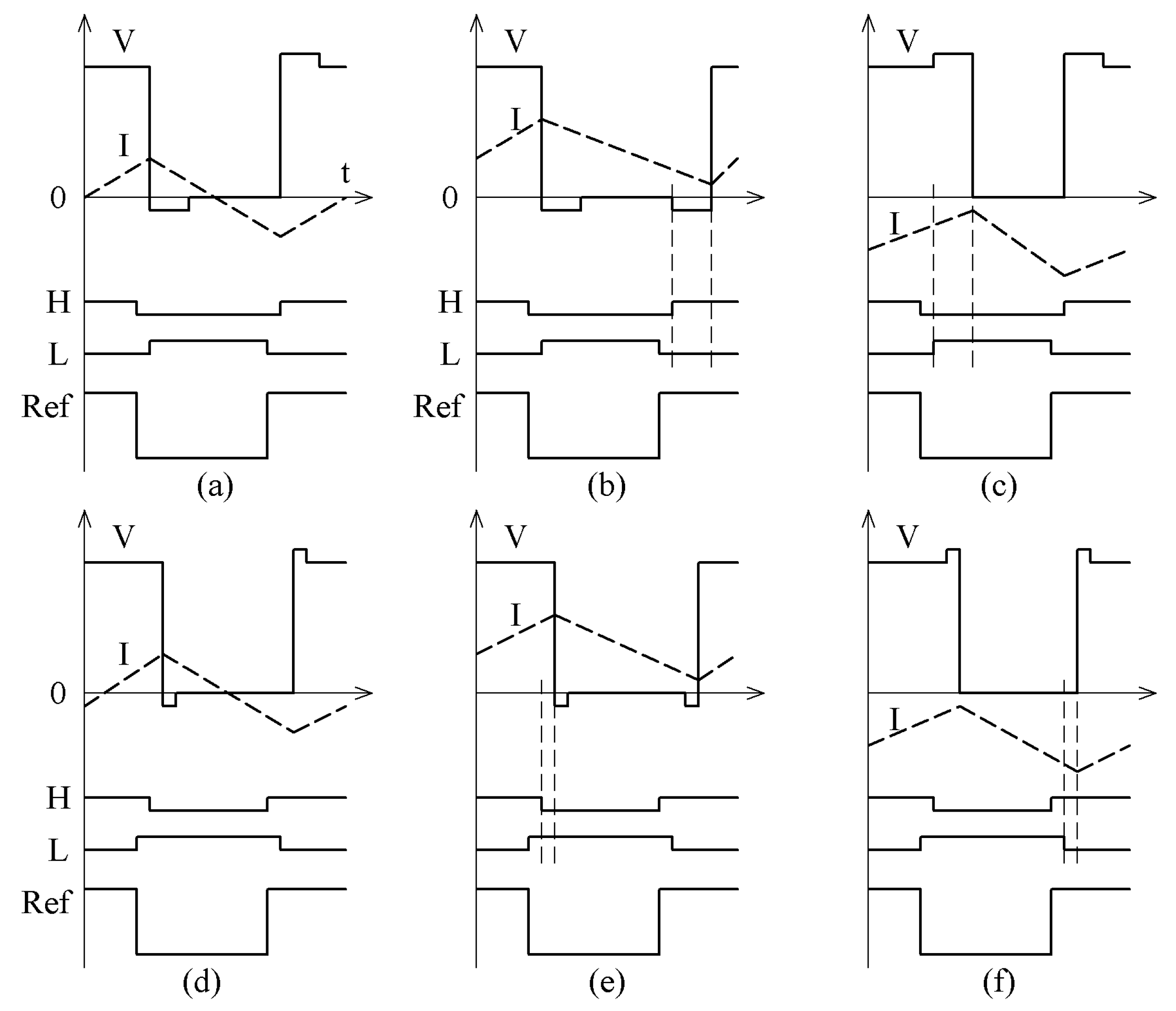
2.1. Dead-Time Generation

Ideally, the output dead-time should be equal to zero to minimize the additional losses [11]. When a fixed dead-time is used, it should be long enough with respect to the driver and transistor switching parameters to prevent a shoot-through (i.e., when both transistors are on simultaneously) [18]. The dead-time in the half-bridge configuration is adjusted by delaying the MCU’s control signal’s rising and falling edges. The set dead-time can be both positive and negative. The negative dead-time is needed in case the turn-on delays are longer than the turn-off delays. This is explained in Figure 2, which shows the reference signal (Ref); the corresponding controllers’ outputs for the high (H) and low (L) transistors, respectively; and the resulting output voltage (V) and current (I) waveforms. The figure shows a situation when the driver and transistor turn-on delay is longer than the turn-off delay. In practice, this situation is common when separate high-side drivers or digital isolators are used during the circuit design [9].
In the so-called discontinuous conduction mode (DCM), the output current polarity changes within a single switching period, causing a voltage commutation that always appears after the previously conducting transistor is turned off [19]. During the DCM, the output duty cycle is not influenced by the dead-time, as seen in Figure 2a,d. The shorter output dead-time in Figure 2d was achieved by utilizing the negative dead-time, which is created by delaying the control signals’ falling edges for both the upper and lower transistors.
In the case of continuous conduction mode (CCM) and the current source operation (Figure 2b), the output signal’s rising edge was delayed by the dead-time plus the difference in the turn-on/off times of the driver’s circuitry. The output duty cycle does not correspond to the reference duty-cycle, which means voltage distortion is introduced. When the half-bridge operates as a current sink (Figure 2c), the falling edge is delayed instead, and the duty cycle is increased.
During CCM and current source operation (Figure 2e), the negative dead-time changes the output duty cycle at the falling edge of the output signal, similar to the situation shown in Figure 2c. For the current sink operation (Figure 2f), the rising edge was adjusted.
Depending on the half-bridge output current in CCM, the output duty cycle D can be obtained from Table 1.
In Table 1, D MCU is the reference duty cycle, t d ( rise ) is the switching delay following the reference signal’s rising edge, t d ( fall ) is the switching delay following the reference signal’s falling edge, and T is the switching period.

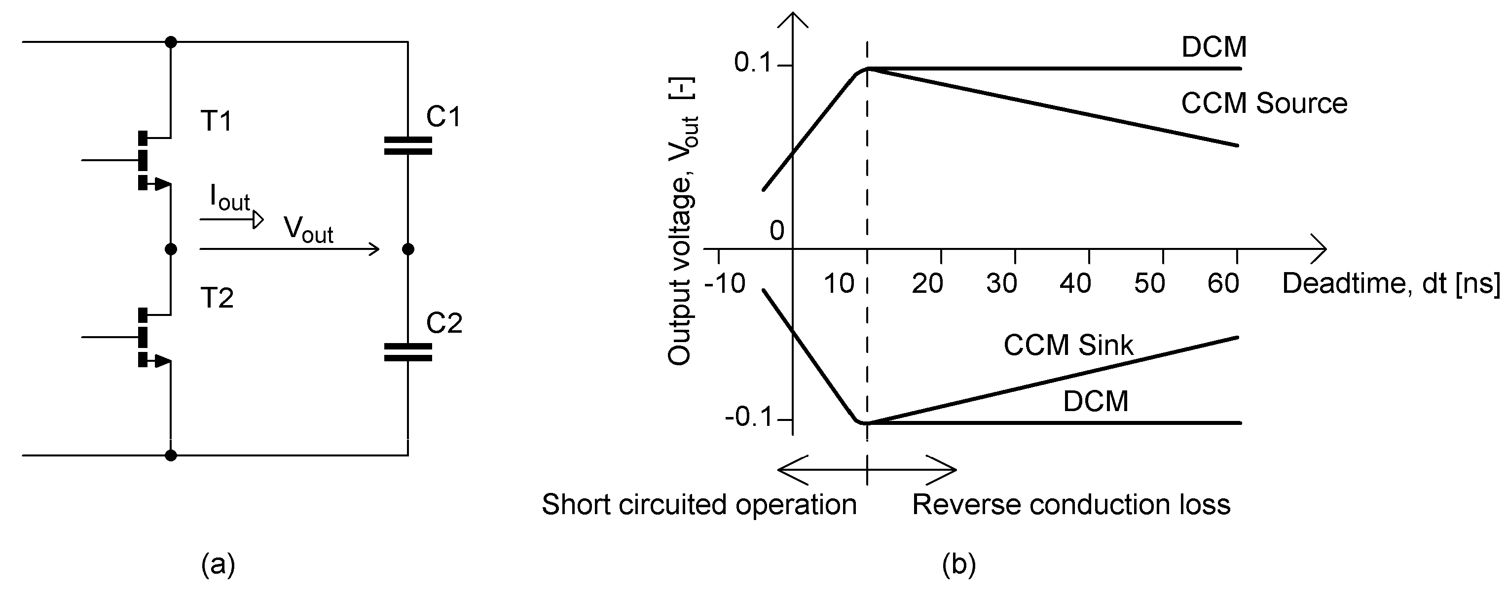
2.2. Reverse Conduction Loss

The cause of the reverse conduction losses is shown in Figure 3. Here, the half-bridge output voltage (which operates as a current source) is distorted by negative peaks that correspond to the low transistor being in the self-commutated reverse conduction region [6]. The peaks disappear when the transistor is turned on and starts to operate with a smaller voltage drop (comparable to the forward conduction mode). The dead-time is at its optimum when the duration of the negative peaks is minimized.
The output voltage V out of the converter can be expressed as [17]
V out = D · V DC Δ V SD ,
Δ V SD = 2 t dt T V SD ( off ) · sgn ( I out ) ,
where D is the output duty cycle, V DC is the DC-link voltage, Δ V SD is the additional voltage drop caused by the non-zero output dead-time, t dt is the output dead-time, V SD ( off ) is the voltage drop across the source and drain, and I out is the converter’s output current.
The additional voltage drop Δ V SD depends on the polarity of the output current and source-drain voltage V SD ( off ) , which appears across the transistor that operates in reverse conduction self-commutated mode. The source-drain voltage V SD ( off ) consists of the gate threshold voltage V GS ( th ) and negative gate voltage V GS ( off ) that the driver applies during the off state [8], i.e.,
V SD ( off ) = V GS ( th ) V GS ( off ) .
From (3), it can be seen that the dead-time losses are even more significant in the case of robust converters that apply a negative gate voltage in the off-state to prevent a false turn-on.
As explained in the previous section, the converter output voltage changes with the dead-time depending on the operation mode (Figure 4). During the CCM, the maximum output voltage exists, which corresponds to no self-commutation. When the dead-time is decreased beyond some threshold value (the vertical dashed line in Figure 4b), the current flowing through the recently turned-on transistor starts to rise before the current of the other transistor drops to zero. This shoot-through operation means the output is connected to the virtual DC-link neutral point for a short time. The current is then limited only by the parasitic inductance.

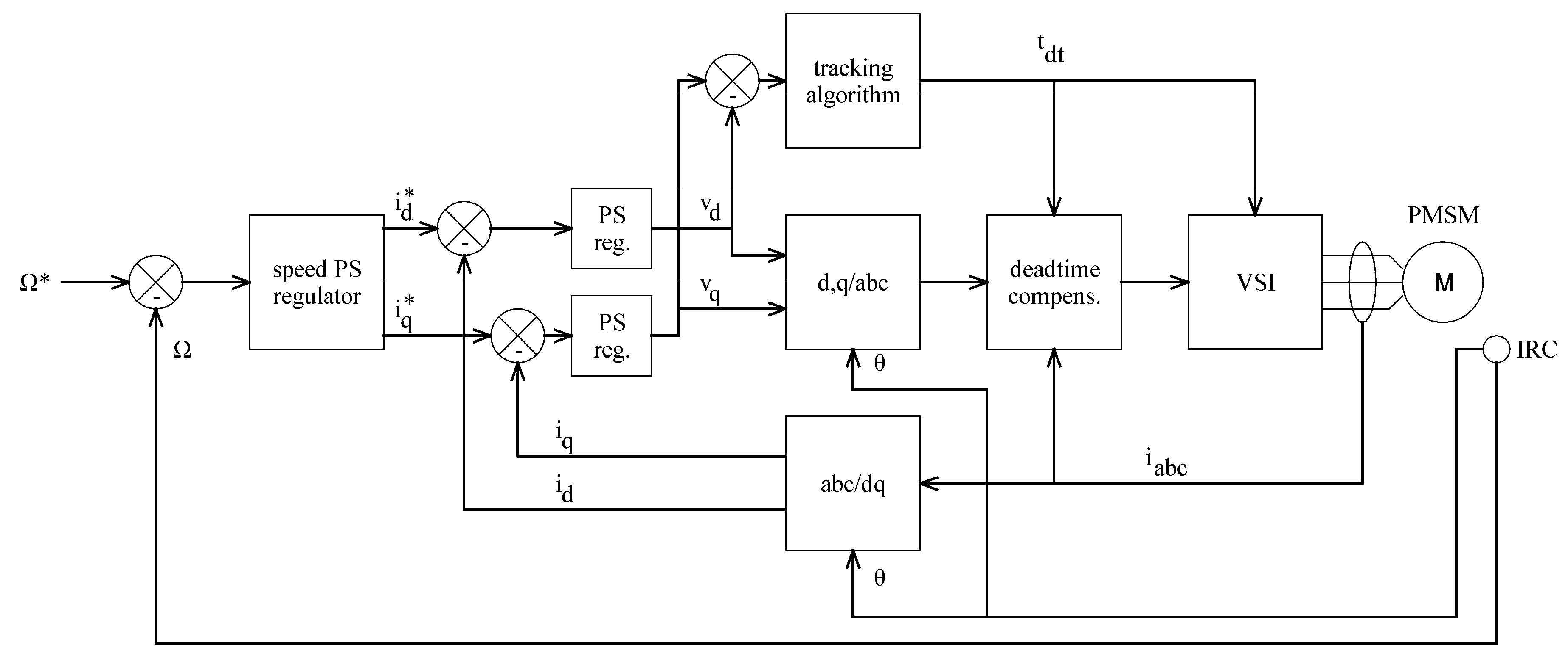
2.3. Drive Controller

The block diagram of the proposed control scheme with a dead-time loss minimization algorithm is presented in Figure 5. In contrast to the standard control schemes, the tracking algorithm block, and the corresponding dead-time compensation block, are added. Figure 5 also shows a speed PS regulator with the possibility of field-weakening operation. Such a controller has been described, for instance, in [20]. The reason behind the PS speed controller deployment is a more convenient measurement and presentation of the experimental results.
In a steady state, the Δ V SD given by (2) produces output voltage distortion that can be expressed as [21]
Δ v α = K 2 t dt T V SD ( off ) [ sgn ( i a ) 1 2 sgn ( i b ) 1 2 sgn ( i c ) ] ,
Δ v β = K 3 2 2 t dt T V SD ( off ) [ sgn ( i b ) sgn ( i c ) ] .
where K is Clarke’s transformation coefficient. The distorting voltage components expressed in the α β stationary reference frame can be transformed into the rotor-fixed d q reference frame as
Δ v d = Δ v α cos ( θ ) + Δ v β sin ( θ ) ,
Δ v q = Δ v β cos ( θ ) Δ v α sin ( θ ) .
where θ is the angle between the stationary and rotor-fixed coordinate systems. Figure 6a shows the trajectory of the reference voltage vector (dashed) and the distorted voltage vector (solid) per electrical revolution in the stationary α β coordinate system (voltage in per unit). Figure 6b then shows the vectors transformed into the d q reference frame. From Figure 6, it can be seen that to compensate for the voltage distortion, the d -axis current controller has to increase the v d * demand, and the q -axis controller has to decrease the v q * demand.

2.4. Tracking Algorithm

The tracking algorithm [15] is a simple perturb-and-observe tracker searching for the minimum output of the d q -axis current controllers by adjusting the dead-time for the VSI. Mathematically, the output of the tracker can be described as
t dt ( k ) = t dt ( k 1 ) + Δ t dt ,
( v q ( av ) v d ( av ) ) k > ( v q ( av ) v d ( av ) ) k 1 Δ t d t = Δ t d t ,
where Δ t dt is the dead-time increment, v d ( av ) and v q ( av ) are the d q voltage components averaged within the tracker update period, and the symbol k denotes the discrete step. The duty cycle for each phase is then compensated according to Table 1, i.e.,
D x = D MCU x + t dt T · sgn ( i x ) ,   x = a , b , c .
The optimum dead-time is continually tracked to ensure the reverse conduction losses are minimized, even during the drive parameter variation (i.e., power, DC-link voltage, and temperature variations).

3. Experimental Results

A GaN-based three-phase VSI prototype was built to implement the motor control algorithm along with the proposed dead-time loss minimization method. A picture of the experimental workspace is shown in Figure 7.
The following experiment was designed to test the method. A PMSM drive was operated under various load and speed conditions, including the field-weakening region. At first, the tracking algorithm input variable had to be determined. Based on the theoretical analysis performed in Section 2, the resulting quantity selected as the tracker’s observed value was the difference between the q - and d -axis voltage components, i.e., v q v d . With the observed variable determined, the tracking algorithm had to be tuned; i.e., the dead-time increment and update period values were set. The tracking algorithm was then tested at multiple operating points. Furthermore, the power consumed by the converter for multiple fixed dead-time values was measured, and the results were compared to the proposed tracker-based optimization method.

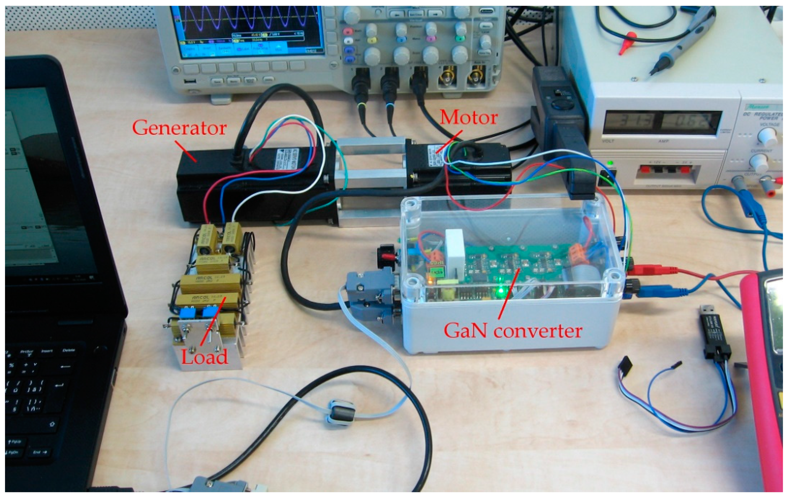
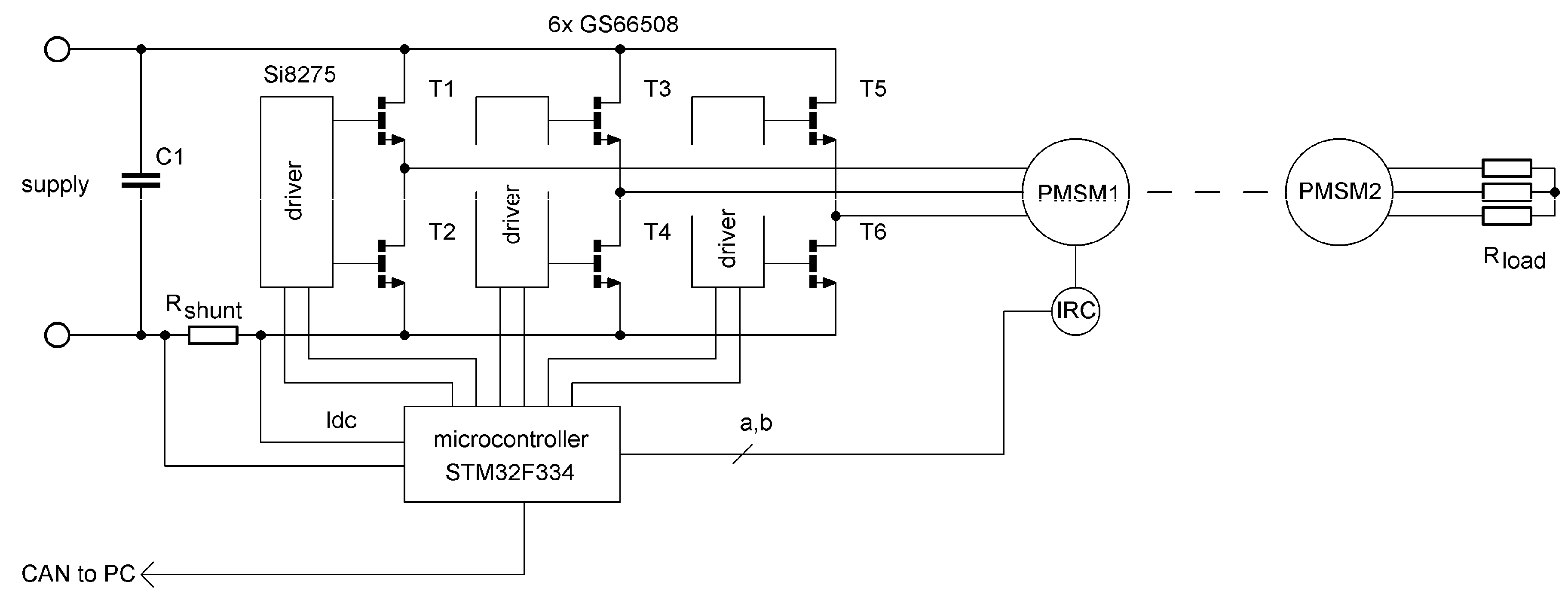
3.1. Experimental Setup

The VSI was equipped with six GS66508T GaN transistors driven by Si8275 isolated half-bridge gate drivers. The converter was controlled by an ARM Cortex M4 MCU STM32F334 equipped with a high-resolution timer peripheral that allows setting the duty cycle and dead-time with a resolution up to 217 ps. The SVM frequency was set to 100 kHz. The converter supplied a 200 W 4-pole PMSM with an incremental encoder used for speed and position feedback. A simplified schematic diagram of the experimental setup is shown in Figure 8.
A single shunt current measuring method with phase current reconstruction optimized for a high switching frequency [22] was used for the current measurement. The VSI output voltage is hardware-demanding to measure directly due to its pulsating nature and high-frequency components. Therefore, the reference voltage vector, i.e., the current controllers’ output, was used within the algorithm instead. The controlled motor was then coupled with a similar PMSM machine loaded by resistors R load to create a mechanical load. The nameplate data and model parameters of both machines are shown in Table 2. The data acquired by the MCU were transferred directly to the laptop via a CAN bus, which was also used to set the controllers’ reference values.

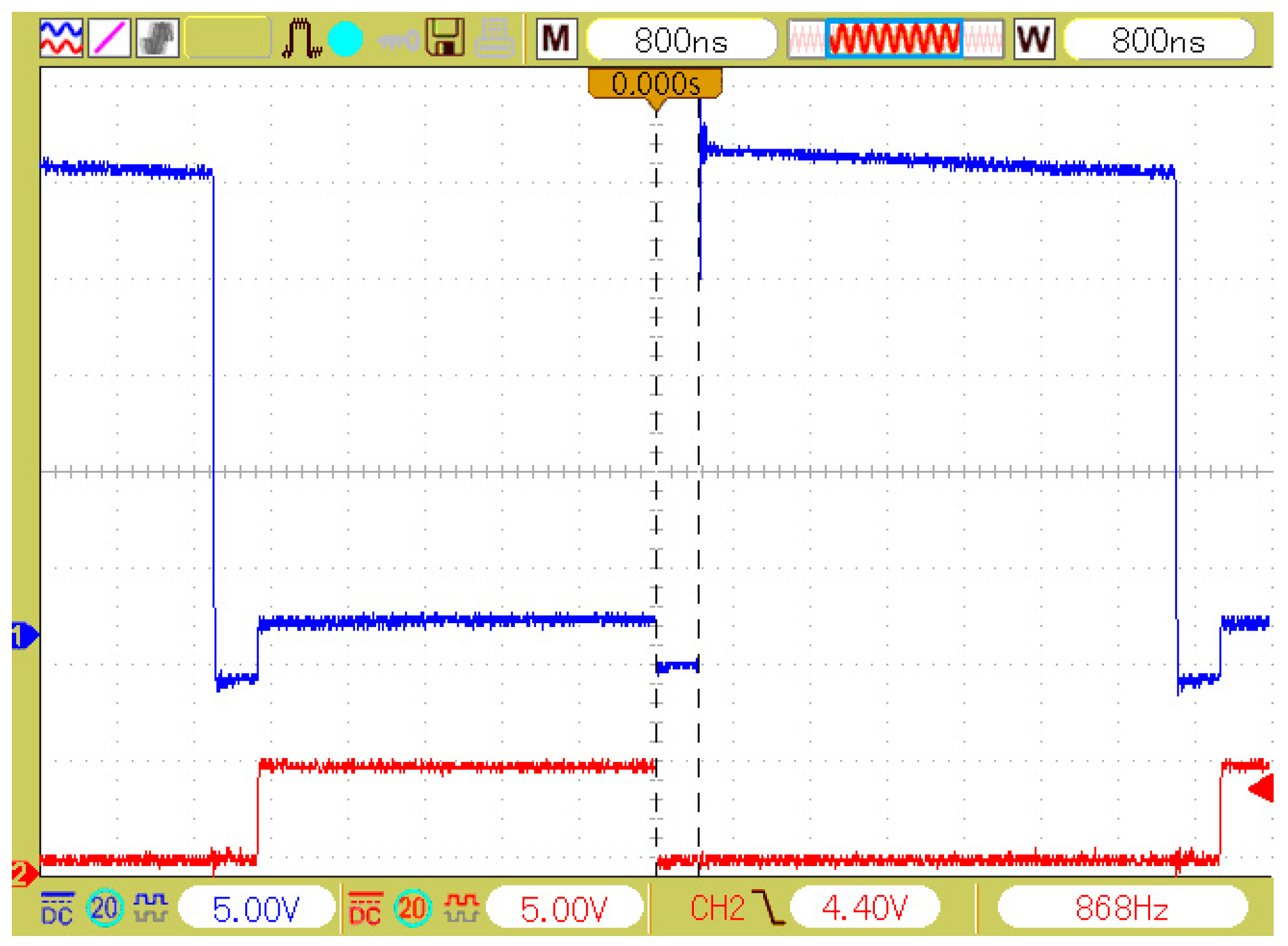
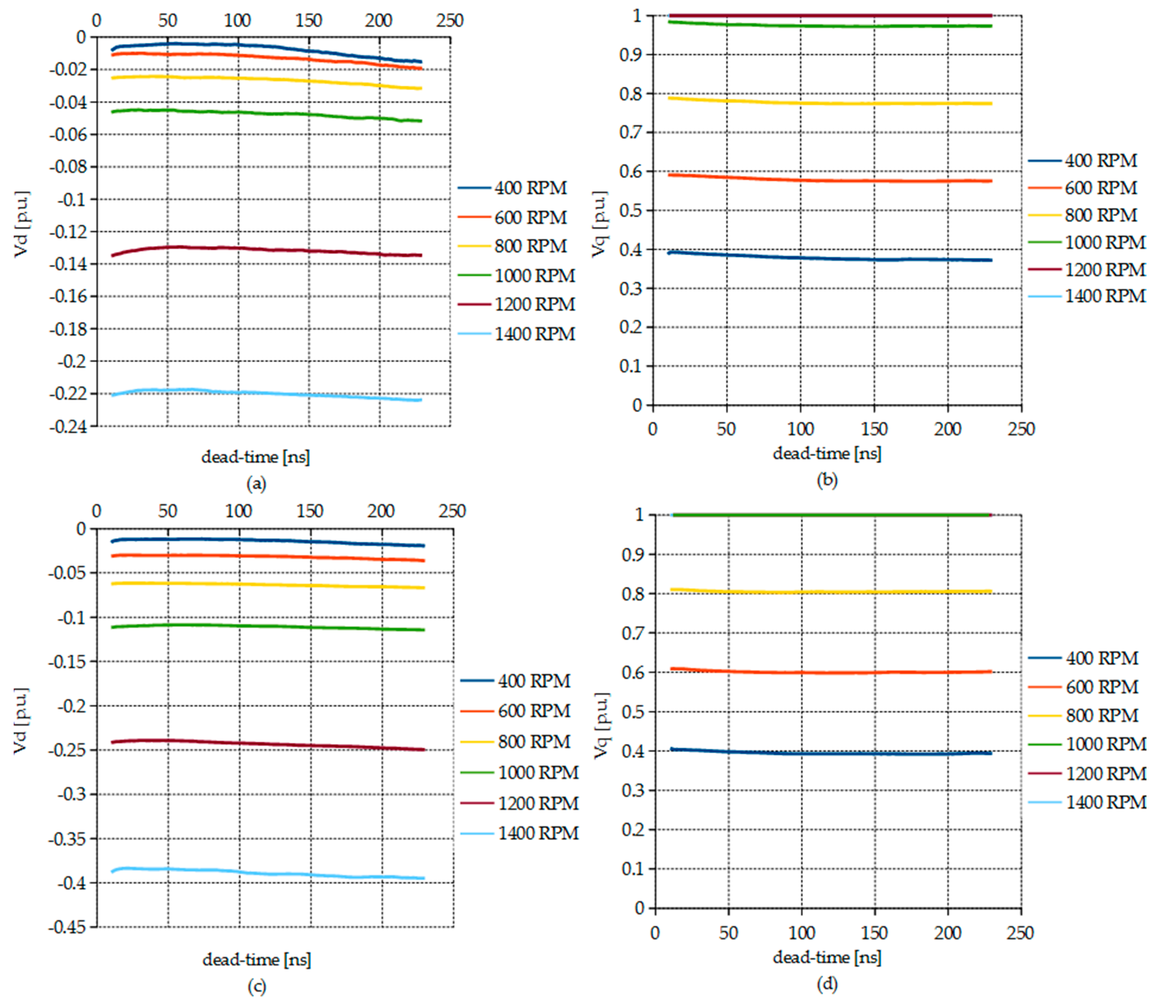
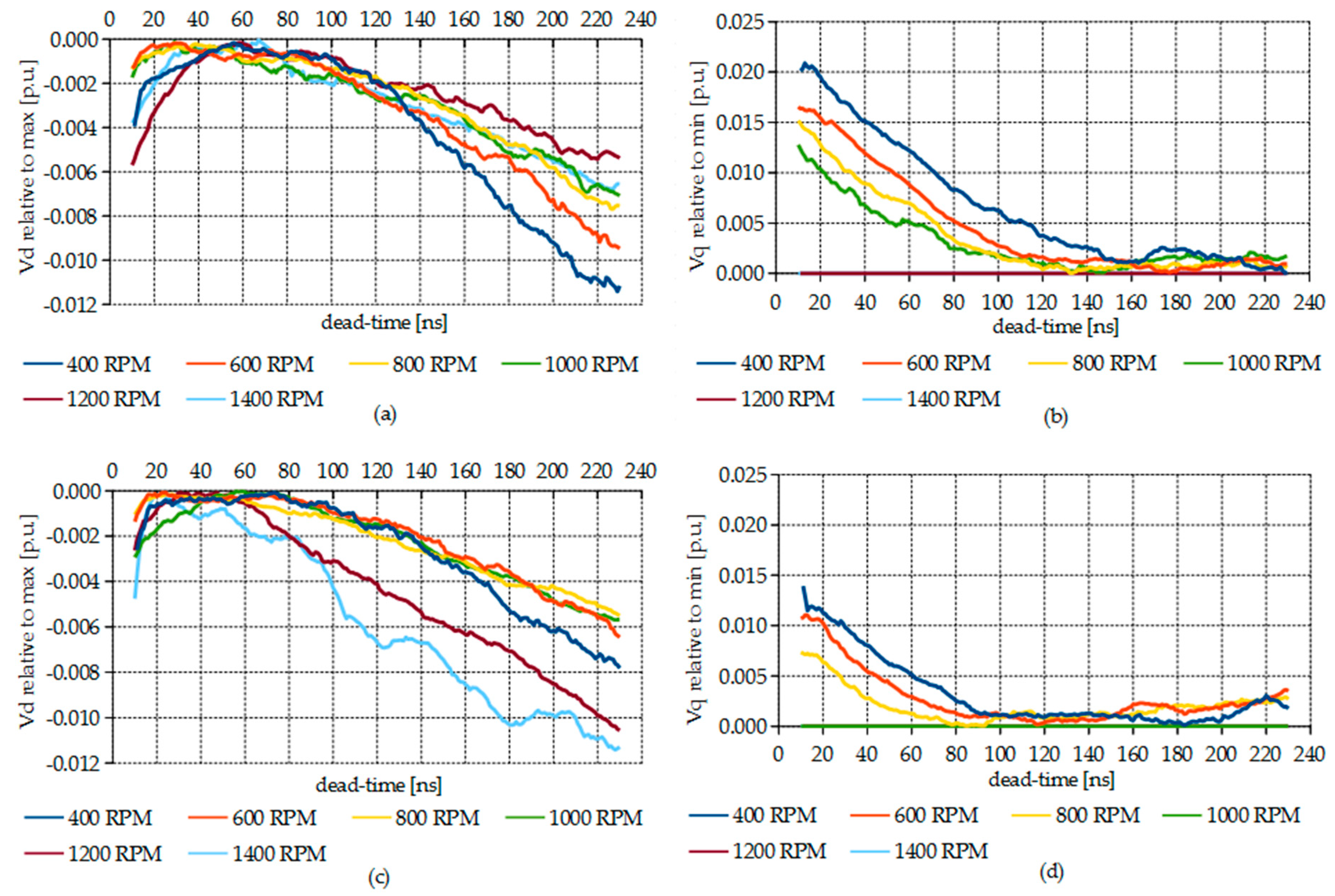
3.2. Current Controllers’ Output Change with Dead-Time

First, the behavior of the current controllers’ output with respect to the set dead-time was examined. During the experiment, the motor was running in a steady state at a constant speed, with the dead-time being changed by 1 ns steps per 200 ms to let the current controllers stabilize. The reference speed was then modified and the data measured again. The dependence of the relative output values of the d - and q -axis current controllers on the set dead-time for different reference speed values and different load resistors R load are plotted in Figure 9.
Figure 9a shows that v d decreased with increasing speed. Contrary to that, v q (Figure 9b) increased with the speed almost linearly until the field-weakening region was reached (above 1000 RPM). In Figure 9c, the higher negative values of v d with respect to the speed were caused by the increased load angle, while the small increase in v q in Figure 9d compensated the stator resistance. To make the shapes of all the curves more clearly visible, they are replotted in Figure 10 with their aligned peaks.
In Figure 10, the v d curves exhibit a visible maximum, while the v q curves mostly keep decreasing across the whole tested range. This behavior was caused by the distorting voltage vector decreasing v d and increasing v q components, as shown in Figure 6. During this time, the reverse conduction losses were increased with the set dead-time. It follows that the optimum dead-time value can be found at the minimum of v q v d . This quantity is also used as the observed value within the tracking algorithm.

3.3. Tracking Algorithm

Figure 11 shows the trace of the tracker’s dead-time from the starting point of 200 ns. The dead-time increment Δ t dt was set to 5 ns, and the tracker update period, to 200 ms. In Figure 11a, the motor was running at 800 RPM where both the v d and v q voltage components were changing. In Figure 11b, the motor was running in the field-weakening region where only the change in v d was observed by the tracker. For an increased load and the same speed references, Figure 11c,d show lower values found by the tracker.
Due to the speed-dependent load, a higher speed means a higher output VSI current. The same goes for an increased load. The VSI current and the current-dependent change in the GaN’s switching behavior caused additional losses and output dead-time variation. Therefore, the optimum dead-time found was lower for both increased loads and speeds.

3.4. Dead-Time Loss Minimization

To quantify the amount of energy savings achieved with the proposed method, the input inverter power was measured for multiple cases. Within the first group of tests, the converter was operated with selected values of fixed dead-time. Within the second group of tests, the converter was operated with a dead-time found by the tracking algorithm. Table 3 shows the measured DC-link currents for the fixed and tracked optimum dead-times with the calculated relative loss differences.
In Table 3, it can be seen that for 400 RPM, the optimum dead-time lies close to 100 ns because here, the relative loss difference between the fixed and tracked dead-time is minimal. A similar situation exists for 1200 RPM and 50 ns. Contrary to that, the fixed 10 ns and 200 ns values were clearly too small and large, respectively, for the whole measured range.
In the field-weakening region (above 1000 RPM), the power loss decrease is more significant because the field-weakening d -axis current component causes additional losses when the dead-time is fixed. This is important mainly when the GaN converter is used as a direct replacement for a silicon-based converter. At high switching frequencies, the GaN reverse conduction mode causes higher power losses compared to low-frequency silicon-based converters. Therefore, it follows that the dead-time optimization is also important from the point of view of the GaN-based converters becoming a convenient high-power density and high-efficiency alternative to silicon-based converters.

3.5. Comparison with Other Methods Mentioned in the Literature

To assess the overall quality of the proposed method within the context of other methods presented in the literature, a qualitative comparison was made. The features of the individual approaches in selected categories are highlighted in Table 4. The method presented in this paper stands out against other approaches mainly because it eliminates their disadvantages while achieving effective loss minimization at the same time.

4. Discussion

In this paper, a novel method of a GaN-based PMSM drive dead-time loss minimization strategy was presented. The proposed control scheme consists of a classic vector control structure with an added tracking algorithm to find the optimum dead-time for GaN transistors. The main idea behind the presented method is based on the theoretical and mathematical analysis of the GaN’s reverse conduction phenomena and their influence on the inverter output voltage. It follows that reverse conduction losses occur together with the output voltage distortion. Therefore, the tracker, a simple perturb-and-observe algorithm, utilizes the current controllers’ voltage outputs for the online optimum dead-time selection. The presented method’s main contribution is that neither additional hardware nor prior inverter data are necessary for its operation. This makes the method a viable option for either “offline” or online optimum dead-time identification.
The experimental results confirm the validity of the presented approach at multiple drive operating points. It has been found out that a load increase leads to a lower optimum dead-time being found by the tracker. This is caused by the current-dependent switching behavior of GaN devices. Furthermore, converter power losses were measured at several operating points for multiple fixed dead-time values and compared to the losses measured for the case of an active dead-time tracker. The results confirm the advantages of the load-dependent optimum dead-time generation over a fixed dead-time. In the field-weakening region, the saved power was more significant due to the PMSM characteristics because less power was dissipated to weaken the permanent magnets’ flux, as the converter’s output voltage was not decreased by the reverse conduction drop at the optimum dead-time.

Author Contributions

Conceptualization, P.S., O.L., and J.L.; methodology, P.S. and J.L.; software, P.S.; validation, P.S.; formal analysis, P.S., F.F., and O.L.; investigation, P.S. and O.L.; resources, P.S. and F.F.; data curation, P.S.; writing—original draft preparation, P.S. and F.F.; writing—review and editing, O.L. and J.L.; visualization, P.S.; supervision, J.L.; project administration, J.L.; funding acquisition, P.S. and F.F. All authors have read and agreed to the published version of the manuscript.

Funding

This research was funded by the Student Grant Agency of the Czech Technical University in Prague, grant number SGS20/164/OHK3/3T/13, SGS20/061/OHK3/1T/13.

Conflicts of Interest

The authors declare no conflict of interest.

References

  1. Chen, K.J.; Häberlen, O.; Lidow, A.; Tsai, C.L.; Ueda, T.; Uemoto, Y.; Wu, Y. GaN-on-Si Power Technology: Devices and Applications. IEEE Trans. Electron. Devices 2017, 64, 779–795. [Google Scholar] [CrossRef]
  2. Shirabe, K.; Swamy, M.M.; Kang, J.-K.; Hisatsune, M.; Wu, Y.; Kebort, D.; Honea, J. Efficiency Comparison Between Si-IGBT-Based Drive and GaN-Based Drive. IEEE Trans. Ind. Appl. 2014, 50, 566–572. [Google Scholar] [CrossRef]
  3. Ding, X.; Zhou, Y.; Cheng, J. A review of gallium nitride power device and its applications in motor drive. CES Trans. El. Mach. Syst. 2019, 3, 54–64. [Google Scholar] [CrossRef]
  4. Deboy, G.; Treu, M.; Haeberlen, O.; Neumayr, D. Si, SiC and GaN power devices: An unbiased view on key performance indicators. In Proceedings of the 2016 IEEE International Electron Devices Meeting (IEDM), San Francisco, CA, USA, 3–7 December 2016. [Google Scholar]
  5. Xie, R.; Wang, H.; Tang, G.; Yang, X.; Chen, K.J. An Analytical Model for False Turn-On Evaluation of High-Voltage Enhancement-Mode GaN Transistor in Bridge-Leg Configuration. IEEE Trans. Power Electron. 2017, 32, 6416–6433. [Google Scholar] [CrossRef]
  6. Sørensen, C.; Fogsgaard, M.L.; Christiansen, M.N.; Graungaard, M.K.; Nørgaard, J.B.; Uhrenfeldt, C.; Trintis, I. Conduction, reverse conduction and switching characteristics of GaN E-HEMT. In Proceedings of the 6th International Symposium on Power Electronics for Distributed Generation Systems (PEDG), Aachen, Germany, 22–25 June 2015. [Google Scholar]
  7. Lee, W.; Han, D.; Choi, W.; Sarlioglu, B. Reducing reverse conduction and switching losses in GaN HEMT-based high-speed permanent magnet brushless dc motor drive. In Proceedings of the 2017 IEEE Energy Conversion Congress and Exposition (ECCE), Cincinnati, OH, USA, 1–5 October 2017. [Google Scholar]
  8. Williford, P.; Jones, E.A.; Yang, Z.; Chen, J.; Wang, F.; Bala, S.; Xu, J. Optimal Dead-time Setting and Loss Analysis for GaN-based Voltage Source Converter. In Proceedings of the 2018 IEEE Energy Conversion Congress and Exposition (ECCE), Portland, OR, USA, 23–27 September 2018. [Google Scholar]
  9. Roschatt, P.M.; McMahon, R.A.; Pickering, S. Investigation of dead-time behaviour in GaN DC-DC buck converter with a negative gate voltage. In Proceedings of the 2015 9th International Conference on Power Electronics and ECCE Asia (ICPE-ECCE Asia), Seoul, Korea, 1–5 June 2015. [Google Scholar]
  10. Joo, D.M.; Byun, J.E.; Lee, B.K.; Kim, J.S. Adaptive delay control for synchronous rectification phase-shifted full bridge converter with GaN HEMT. Electron. Lett. 2017, 53, 1541–1542. [Google Scholar] [CrossRef]
  11. Schirone, L.; Macellari, M.; Pellitteri, F. Predictive dead time controller for GaN-based boost converters. IET Power Electron. 2017, 10, 421–428. [Google Scholar] [CrossRef]
  12. Dyer, J.; Zhang, Z.; Wang, F.; Costinett, D.; Tolbert, L.M.; Blalock, B.J. Dead-time optimization for SiC based voltage source converters using online condition monitoring. In Proceedings of the 2017 IEEE 5th Workshop on Wide Bandgap Power Devices and Applications (WiPDA), Albuquerque, NM, USA, 30 October–1 November 2017. [Google Scholar]
  13. Zhang, Y.; Chen, C.; Liu, T.; Xu, K.; Kang, Y.; Peng, H. A High Efficiency Model-Based Adaptive Dead-Time Control Method for GaN HEMTs Considering Nonlinear Junction Capacitors in Triangular Current Mode Operation. IEEE Emerg. Sel. Power Electron. 2020, 8, 124–140. [Google Scholar] [CrossRef]
  14. Han, D.; Sarlioglu, B. Deadtime Effect on GaN-Based Synchronous Boost Converter and Analytical Model for Optimal Deadtime Selection. IEEE Trans. Power Electron. 2016, 31, 601–612. [Google Scholar] [CrossRef]
  15. Abu-qahouq, J.A.; Mao, H.; Al-atrash, H.J.; Batarseh, I. Maximum Efficiency Point Tracking (MEPT) Method and Digital Dead Time Control Implementation. IEEE Trans. Power Electron. 2006, 21, 1273–1281. [Google Scholar] [CrossRef]
  16. Chiu, P.K.; Wang, P.Y.; Li, S.T.; Chen, C.J.; Chen, Y.T. A GaN driver IC with novel highly digitally adaptive dead-time control for Synchronous Rectifier Buck Converter. In Proceedings of the 2020 IEEE Energy Conversion Congress and Exposition (ECCE), Detroit, MI, USA, 11–15 October 2020. [Google Scholar]
  17. Skarolek, P.; Lettl, J. Tracking Dead-time Algorithm for GaN DC/DC Converter. In Proceedings of the 2019 International Conference on Applied Electronics (AE), Pilsen, Czech Republic, 10–11 September 2019. [Google Scholar]
  18. Moradpour, M.; Serpi, A.; Gatto, G. Dead-Time Analysis of a Universal SiC-GaN-Based DC DC Converter for Plug-In Electric Vehicles. In Proceedings of the IECON 2018—44th Annual Conference of the IEEE Industrial Electronics Society, Washington, DC, USA, 21–23 October 2018. [Google Scholar]
  19. Spence, K.; Chang, L.; Shao, R. Robust Compensation of Dead Time in DCM for Grid Connected Bridge Inverters. In Proceedings of the 2018 IEEE International Power Electronics and Application Conference and Exposition (PEAC), Shenzhen, China, 4–7 November 2018. [Google Scholar]
  20. Zhou, K.; Ai, M.; Sun, D.; Jin, N.; Wu, X. Field Weakening Operation Control Strategies of PMSM Based on Feedback Linearization. Energies 2019, 12, 4526. [Google Scholar] [CrossRef] [Green Version]
  21. Lipcak, O.; Bauer, J. Analysis of Voltage Distortion and Comparison of Two Simple Voltage Compensation Methods for Sensorless Control of Induction Motor. In Proceedings of the 2019 IEEE 10th International Symposium on Sensorless Control for Electrical Drives (SLED), Turin, Italy, 9–10 September 2019. [Google Scholar]
  22. Park, C.-H.; Kim, D.-Y.; Yeom, H.-B.; Son, Y.-D.; Kim, J.-M. A Current Reconstruction Strategy Following the Operation Area in a 1-Shunt Inverter System. Energies 2019, 12, 1423. [Google Scholar] [CrossRef] [Green Version]
Figure 1. A typical gallium nitride (GaN)-based half-bridge configuration.
Electronics 09 01973 g001
Figure 2. Output duty cycle for (a) discontinuous conduction mode (DCM) positive dead-time, (b) continuous conduction mode (CCM) current source positive dead-time, (c) CCM current sink positive dead-time, (d) DCM negative dead-time, (e) CCM current source negative dead-time, and (f) CCM current sink negative dead-time.
Electronics 09 01973 g002
Figure 3. Half-bridge output voltage (blue) and low-side transistor gate signal (red).
Electronics 09 01973 g003
Figure 4. Output voltage dependence on dead-time: (a) virtual DC-link neutral point, (b) dependence of output voltage on dead-time and modes of operation.
Electronics 09 01973 g004
Figure 5. Proposed control scheme.
Electronics 09 01973 g005
Figure 6. The inverter reference (dashed) and distorted (solid) output voltage in (a) the stationary α β reference frame and (b) in the rotor-fixed d q reference frame; t dt = 5 % of T ; Δ V SD = 5 % of V DC ; power factor, 0.5 ; load angle, 15°.
Electronics 09 01973 g006
Figure 7. Experimental workspace.
Electronics 09 01973 g007
Figure 8. Simplified schematic diagram of the experimental setup.
Electronics 09 01973 g008
Figure 9. Dependence of current controllers’ outputs on the set dead-time for different speed references; mechanical load created by PMSM with a variable resistance R load in the armature: (a) d -axis current controller, R load = 187   Ω ; (b) q -axis current controller, R load = 187   Ω ; (c) d -axis current controller, R load = 73   Ω ; and (d) q -axis current controller, R load = 73   Ω .
Electronics 09 01973 g009
Figure 10. More detailed depiction of curves from Figure 9: (a) d -axis current controller, R load = 187   Ω ; (b) q -axis current controller, R load = 187   Ω ; (c) d -axis current controller, R load = 73   Ω ; and (d) q -axis current controller, R load = 73   Ω .
Electronics 09 01973 g010
Figure 11. Tracking algorithm searching for an optimum dead-time for (a) 800 RPM, R load = 187   Ω ; (b) 1200 RPM, R load = 187   Ω ; (c) 800 RPM, R load = 73   Ω ; and (d) 1200 RPM, R load = 73   Ω .
Electronics 09 01973 g011
Table 1. Output duty cycle in CCM.
Current DirectionDead-Time PolarityOutput Duty Cycle
SourcePositive D = D MCU t d ( rise ) T
SourceNegative D = D MCU t d ( fall ) T
SinkPositive D = D MCU + t d ( fall ) T
SinkNegative D = D MCU + t d ( rise ) T
Table 2. Motor and generator parameters.
MotorGenerator
TypeSGM-02A5FSGM-04AW12
RPM30003000
Power (W)200400
Max voltage (V)200200
Max current (A)2.04.0
Stator resistance (Ω)1.351.26
d -axis inductance (mH)7.057.75
q -axis inductance (mH)7.258.05
Table 3. Relative comparison of VSI losses for selected values of fixed dead-time compared to optimized dead-time for various speed references and R load = 73   Ω .
RPMInput DC-Link Current for Various Dead-Time Values (A)Relative Power Saved with the Tracking Algorithm (%)
200 ns 100 ns 50 ns 10 ns Tracker on 200 ns 100 ns 50 ns 10 ns
4000.14160.14090.14190.14780.1409−0.50−0.01−0.71−4.90
6000.23760.23640.23730.24400.2362−0.59−0.08−0.47−3.30
8000.36580.36410.36430.37500.3636−0.61−0.14−0.19−3.14
10000.53380.53100.53010.54000.5293−0.85−0.32−0.15−2.02
12000.76410.76000.75740.77000.7573−0.90−0.36−0.01−1.68
12500.87030.86560.86420.87550.8621−0.95−0.41−0.24−1.55
13000.98320.97480.97090.98300.9682−1.55−0.68−0.28−1.53
13501.07501.0671.06201.07801.0580−1.61−0.85−0.38−1.89
14001.13851.13091.12581.1361.118−1.83−1.15−0.70−1.61
Table 4. Dead-time optimization method comparison.
Additional MeasurementsSimulation RequirementsHWSWLoss Minimization
Fixed Dead-time [18]single measurement---low
Look-Up Table [10]dead-time map required-memory spacesearching in the dead-time mapmedium
Model-Based [13]-converter model preparation-converter model online calculationhigh
Dead-Time Sensor [11]--reverse drop sampling circuitreverse drop data acquisitionhigh
Method Proposed in This Paper---tracking algorithmhigh
Publisher’s Note: MDPI stays neutral with regard to jurisdictional claims in published maps and institutional affiliations.

