1. Introduction
Nitride alloys containing indium are being widely employed in the fabrication of blue light-emitting diodes (LEDs) and laser diodes (LDs). Owing to the wide operating limits and high reliability of GaN devices, several research groups have started investigating the use of GaN as a material for the fabrication of photodetectors and solar cells. Early devices were based on the simple p-n and p-i-n approach; recently, more complex structures were considered, based on InGaN/GaN Multiple Quantum Wells (MQW) or SuperLattices (SL) [
1].
These structures have been experimentally studied by varying the epitaxial design, the thickness of the barriers [
2,
3,
4], the number of quantum wells [
5], and the alloy composition [
6]. In addition, the dependence of the performance and the main operative parameters of the devices were investigated under different conditions, for example, light concentration [
7,
8] or temperature [
9,
10]. The high reliability of this kind of structures in harsh environments [
11] and under very high illumination densities [
12] enables them to be used for novel applications, such as high-power photodetectors or receivers for Li-Fi systems and wireless energy transmission [
13], also in space applications. Similar structures may be of interest also for the design of GaN-based solar cells.
Despite the great potential of InGaN/GaN-based photodetectors and solar cells, no comprehensive analysis of the physical mechanisms that limit the performance of such devices has been published so far in the literature. Moreover, several applications require a study of these devices under monochromatic excitation and very high power [
13,
14,
15]. In literature, these kinds of structures have been analyzed mainly under solar AM0 or AM1.5 illumination with excitation ranging from one sun to few hundreds of sun [
7,
8,
12] and there are very few studies under monochromatic excitation [
16]. Simulative approaches were used to understand the transport model inside the solar cells [
17,
18].
The aim of this paper is to contribute to the understanding in this field, by presenting an extensive analysis of the dependence of the main parameters of MQW InGaN photodetectors (short-circuit current, open-circuit voltage, quantum efficiency) on the operating conditions (excitation density, temperature) under monochromatic 405 nm illumination. We investigate how Shockley–Read–Hall (SRH) recombination, thermionic escape, and carrier tunneling contribute to the overall cell efficiency in the various temperature and excitation regimes, and describe the related trends. We propose a semi-quantitative recombination-escape model based on these considerations and we use it to fit experimental data.
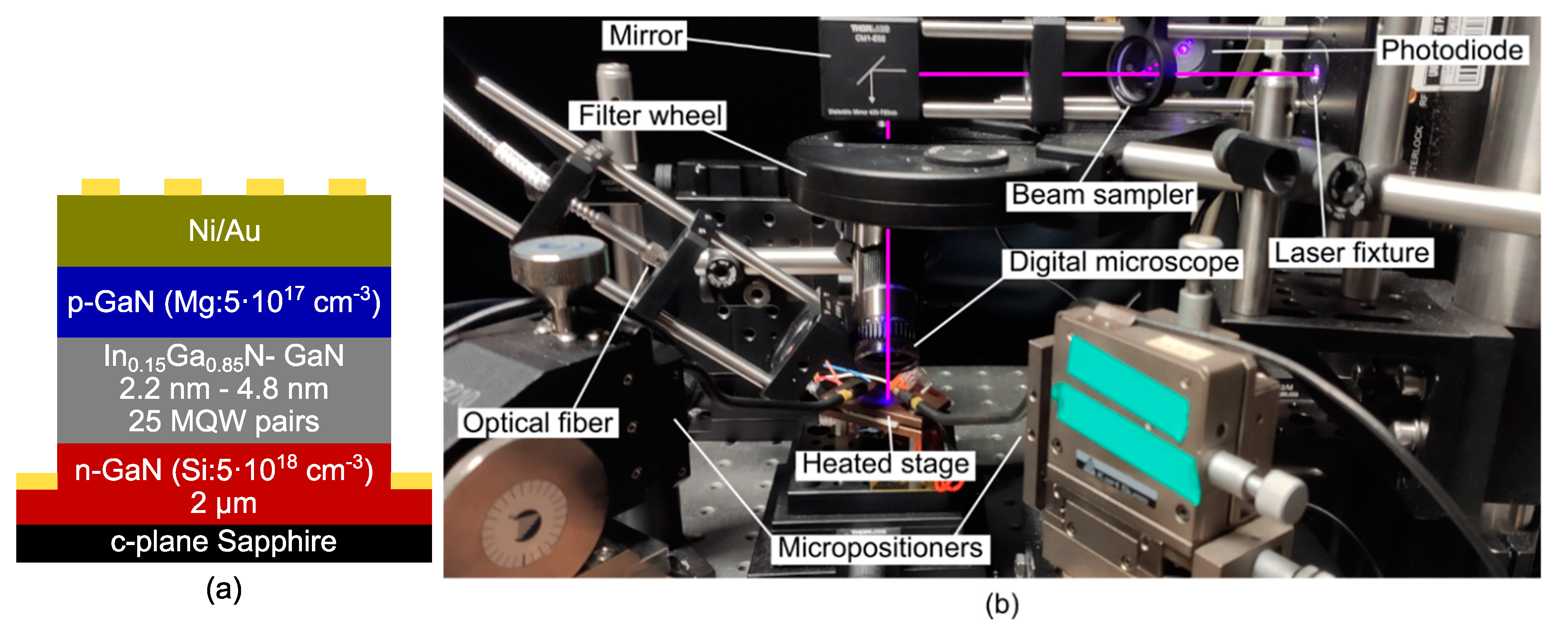
2. Materials and Methods
The samples under test are based on a p-GaN–i-In
0.15Ga
0.85N–n-GaN MQW structure, grown on c-plane sapphire by metal-organic chemical vapor deposition. Over the sapphire substrate, there is a 2 µm thick n-GaN (Si doping 5 × 10
18 cm
−3) layer, over which there is the MQW structure made by 25 periodical layer GaN (4.8 nm thick)–In
0.15Ga
0.85N (2.2 nm thick), topped with a 100 nm thick p-GaN (Mg doping 5 × 10
17 cm
−3) layer. The structure is schematized in
Figure 1a. The approximate density of dislocation was derived to be 2.7 × 10
8 cm
−2 and InGaN quantum wells were determined to be pseudomorphic grown on GaN layer with biaxial strain. Additional details on device structure can be found in previous reports [
19,
20]. The device under test is a 1 mm × 1 mm photodetector.
The device under test (DUT) was connected through tungsten microtips mounted on x-y-z micropositioners and the I–V curves of the devices were collected by means of a HP 4155A Semiconductor Parameter Analyzer. A 405 nm GaN-based LD (nominal optical output power > 2 W), mounted in a Thorlabs TCLDM9 Peltier-cooled fixture and controlled by a Thorlabs ITC4005 controller, was used as light source for illuminated I–V characterization. The spot size was determined to be around 1.41 × 0.15 mm2 by optical measurements. Optical intensity was controlled by changing the driving current of the laser diode. In addition to this, to obtain very low intensities, neutral optical density filters were used (Thorlabs NE05A and NE2A, with optical densities of 0.5 and 2 respectively). The laser intensity was calibrated by means of a Thorlabs S142C integrating sphere. A Thorlabs BSF10-A fused silica beam sampler was employed to redirect a portion of the optical beam on a Thorlabs PDA36A photodiode to obtain feedback on the illumination intensity.
Photocurrent characterization was carried out by using a wide-spectrum 300 W gas discharge xenon lamp, coupled with a Newport CS130 1/8m grating monochromator. The photocurrent signal was amplified by a Merlin lock-in amplifier. The device temperature was controlled by a Thorlabs HT24S2 ceramic heater, driven by a Thorlabs TC200 controller. The experimental set-up is shown in
Figure 1b.
By using pulsed measurements the illuminated I–V curves were measured. From these curves, the short-circuit current (i.e., the current a 0 V), the open-circuit voltage (i.e., the voltage required to have no current flowing in the device) and the maximum power (i.e., the IxV product) were calculated at the various intensities and baseplate temperatures. The optical-to-electrical power conversion efficiency was calculated as the ratio between the maximum electrical power that can be extracted from the cell and the optical power delivered to the cell. From photocurrent measurements at 0 V, the spectral external quantum efficiency (EQE) was calculated by means of a previous calibration of the system.
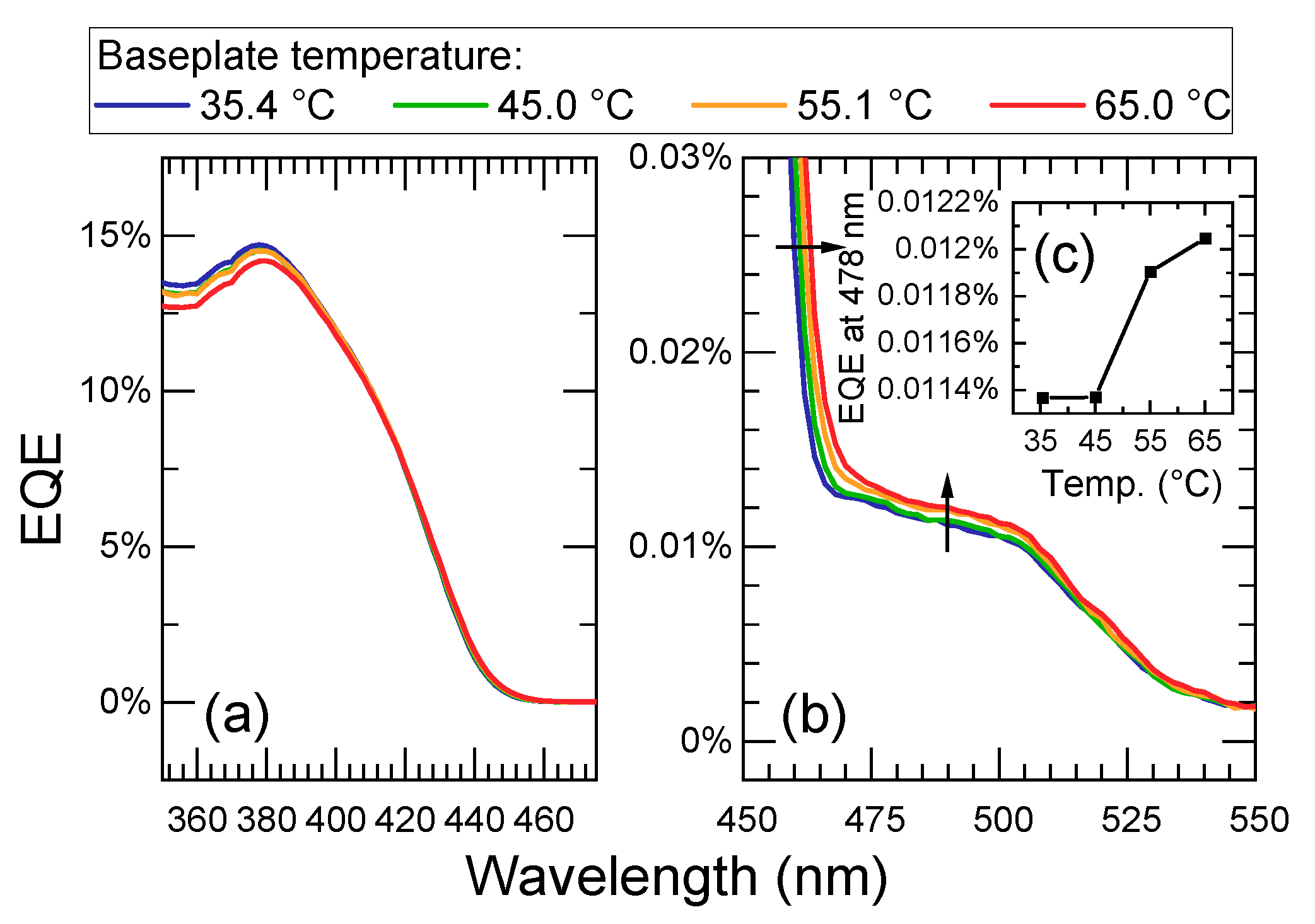
3. Results
The DUTs were characterized by means of spectral photocurrent measurements at different temperatures ranging from 25 °C to 65 °C, allowing to calculate external quantum efficiency, shown in
Figure 2. With increasing temperature, we observed two main changes: (1) a decrease in the peak quantum efficiency, at about 380 nm, and (2) an increase in the quantum efficiency in the yellow band region, below 475 nm (see
Figure 2c). The first effect is ascribed to the increase in SRH non-radiative recombination, which reduces the amount of photogenerated hole–electron pairs that can be extracted from the MQW structure. The second effect can be attributed to an increased emission of carriers from the deep levels responsible for yellow luminescence in GaN (E
C—0.9 eV), typically carbon [
21], V
Ga-O complexes [
22] or V
Ga-H [
23]. By increasing temperature, we also noticed a shift of the band-to-band absorption of the InGaN (edge around 465 nm), that is ascribed to bandgap narrowing. The edge shift has been fitted to estimate the Varshni law parameters with the formula
finding
Eg(0) = 2.83 eV,
α = 0.324 meV/K and
β = 571 K. The value for
Eg(0) is in good agreement with the value calculated in [
24] for In
0.15Ga
0.85N.
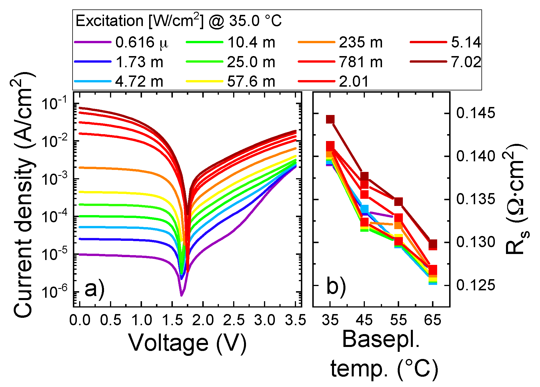
The DUT was characterized under 405 nm monochromatic light at different excitation densities ranging from 616 µW/cm
2 to 7.02 W/cm
2.
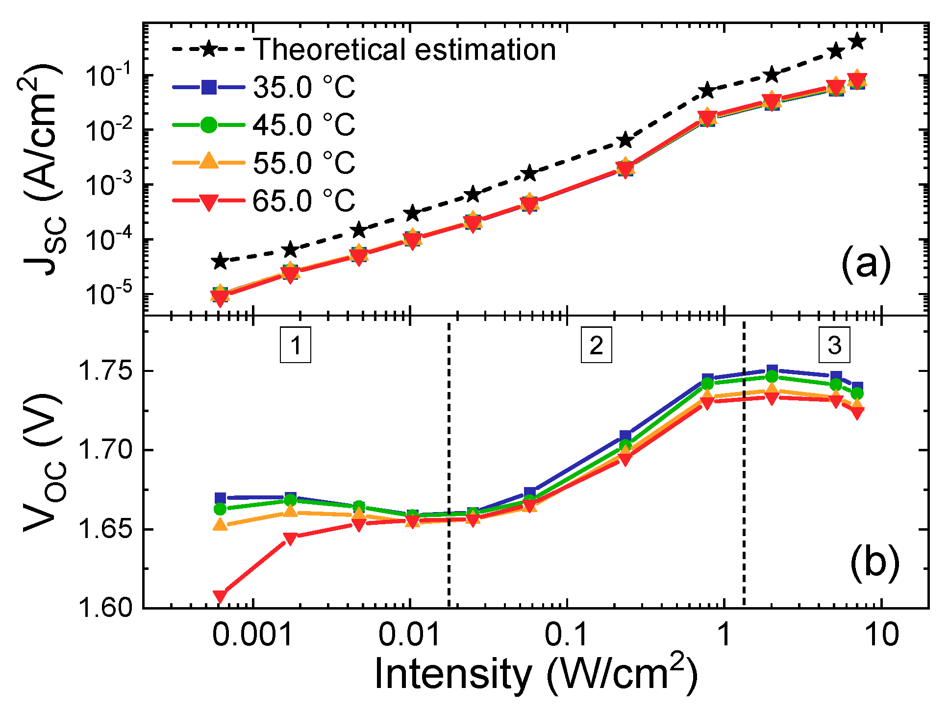
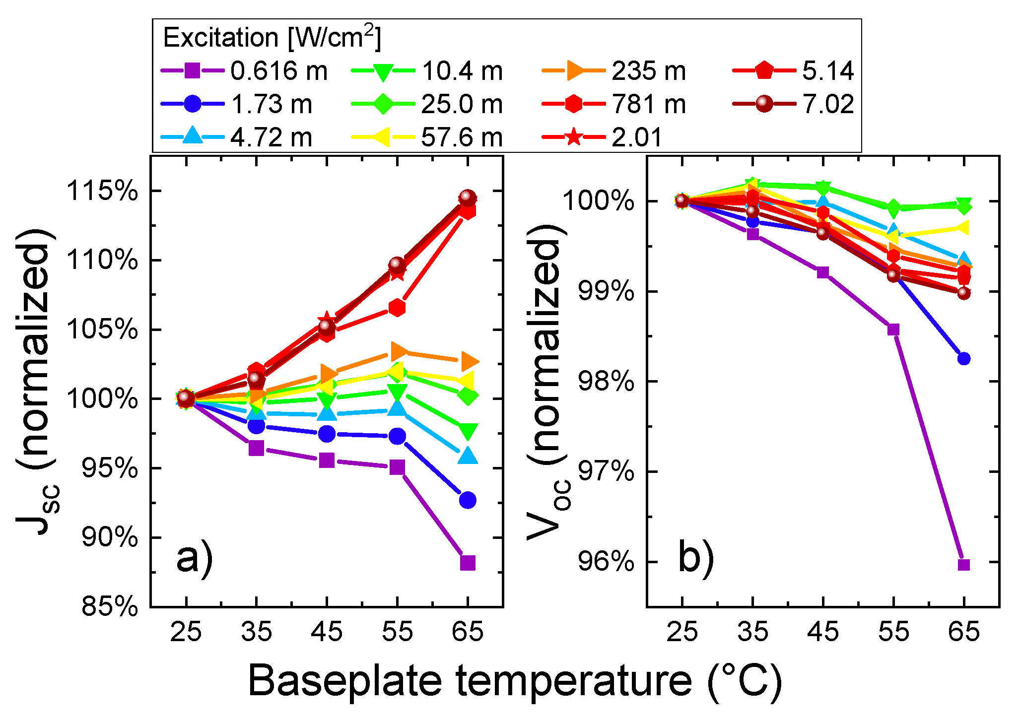
Figure 3 reports the I–V curves obtained from this analysis. By increasing excitation density, the short-circuit current density
JSC (
Figure 4a) increases (in absolute value) from 10
−5 A/cm
2 to 10
−1 A/cm
2. There is a linear relationship between excitation density and short-circuit current, meaning that in short-circuit condition the incoming photons are converted into electron–hole pairs that can be extracted from the device with minimum loss. To obtain a rough evaluation of the losses in the analyzed devices, we estimated the ideal theoretical value of
JSC by calculating the power
Pabs absorbed by the InGaN quantum wells by the Lambert–Beer law and dividing it by the photon energy
Eph. In a best-case scenario, we assumed a unit internal quantum efficiency and extraction efficiency (i.e., every absorbed photon generates an electron–hole pair that is extracted from the device with no loss) and we considered the reflection only at the upper air–GaN interface with reflection coefficient R, thus multiplying the optical power on the device
P0 by the factor 1-R, that is the fraction of light that is not reflected and goes through the air–GaN interface. We obtained the formula:
where
Eph = 3.06 eV,
R = 0.184 (assuming n
GaN = 2.5 [
25]), N is the number of quantum wells,
is the absorption coefficient for 2.2 nm In
0.15Ga
0.85N quantum wells, that can be estimated to be around 10
4 cm
−1 [
26], and
Lw is the well thickness. The calculated theoretical value is approximately four times higher than the experimental value. This result indicates the existence of parasitic recombination paths, as described above, and a non-ideal carrier extraction, and suggest possible pathways for device optimization.
Figure 4b shows that with increasing excitation level, the open-circuit voltage increases significantly (from 1.65 V to 1.75 V), until saturation is reached.
Figure 5 shows that the main trend is a lowering of
VOC with increasing temperature, by an amount dependent on the excitation density. To better understand these results, we consider that a photodetector can be modeled as a diode (the p—n junction) in parallel with a current generator (the photogenerated charge). When the device is in open-circuit,
V =
VOC, the open-circuit voltage can be written as:
The open-circuit voltage is logarithmically proportional to one plus the ratio between the photogenerated current (IL) and the reverse saturation current (IS), according to Equation (3).
Referring to
Figure 4b, at low excitation (region 1) the photogenerated carriers incur in SRH recombination and thus the open-circuit voltage is constant and decreases with increasing temperature. At intermediate excitation densities, SRH recombination saturates and the open-circuit voltage increases logarithmically (region 2), since the density of light-generated carriers increases, and remains constant by increasing temperature. At very high excitation densities (region 3) the open-circuit voltage saturates, possibly due to band filling effects, since incoming photons cannot generate more charge inside the quantum wells and thus the potential needed to have an open-circuit condition (i.e., no current) becomes constant. The self-heating of the device can also contribute, causing a slight reduction in the open-circuit voltage. The lowering in the V
OC in this regime can be possibly due to the additional contribution of bandgap narrowing and enhanced carrier escape in this high-occupancy condition.
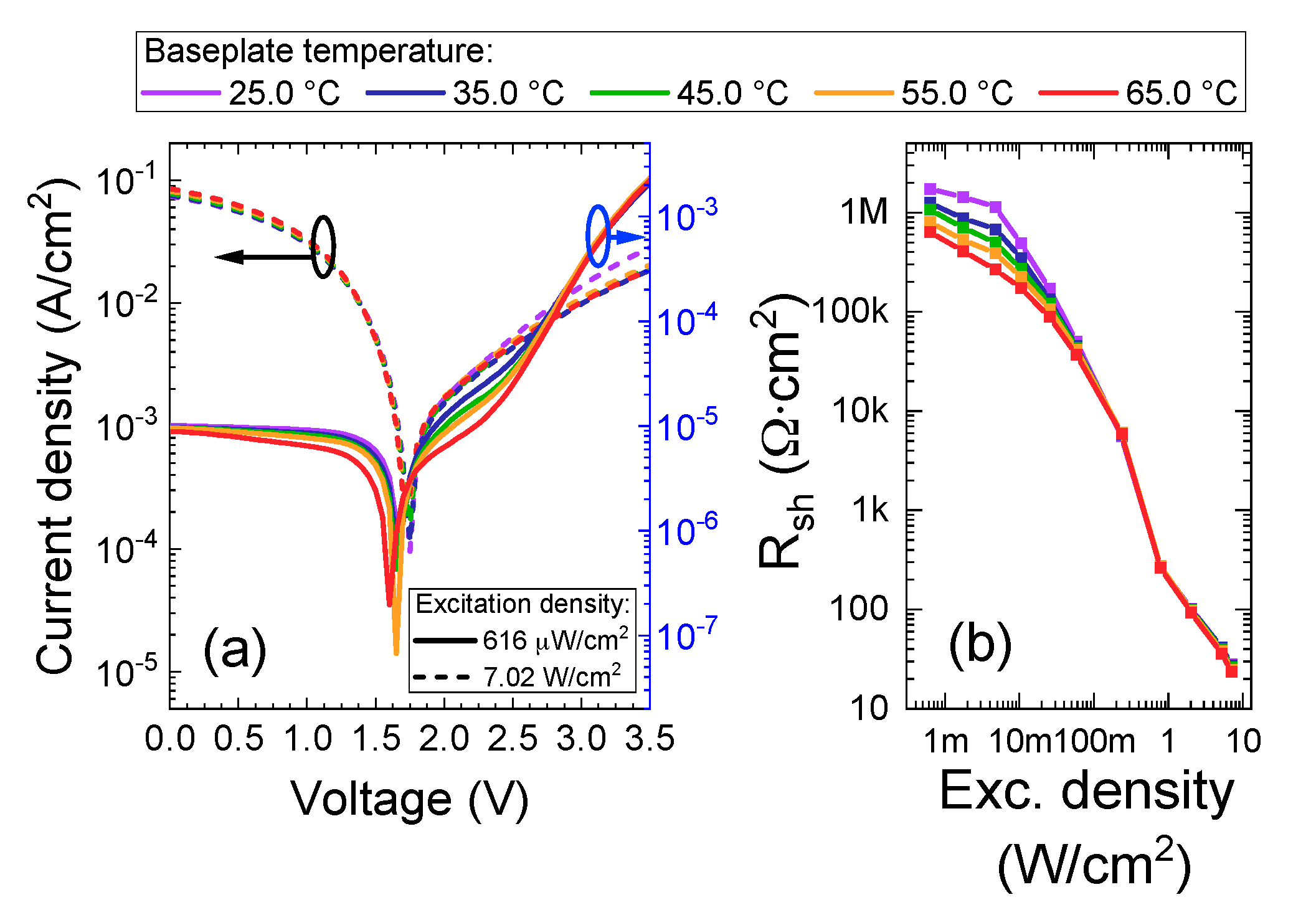
In
Figure 6a, I–V curves at various temperatures for the two extremal excitation densities are plotted. The solid lines correspond to a very low excitation density of 616 µW/cm
2; in the range between 0 V and 1.5 V (i.e., when the electrical power can be extracted from the cell and thus the cell acts as a current generator), the short-circuit current is around 10 µA/cm
2. For higher voltages, i.e., when the cell absorbs current, the IV curves show a double-slope behavior, with an inflexion around 2.6 V. Such effect can be ascribed to the presence of two conduction processes, the first (for voltages lower than 2.6 V) being related to the presence of lattice defects within the active region. By increasing temperature, the reverse (photogenerated) current slightly decreases, possibly due to the stronger recombination occurring through Shockley–Read–Hall processes, which results in stronger carrier losses [
27]. On the other hand, at the highest excitation density (7.02 W/cm
2), a very high photogenerated current is measured. In addition, the defect-related components are not visible in the forward-regime, possibly due to the saturation of non-radiative recombination by the high density of injected carriers.
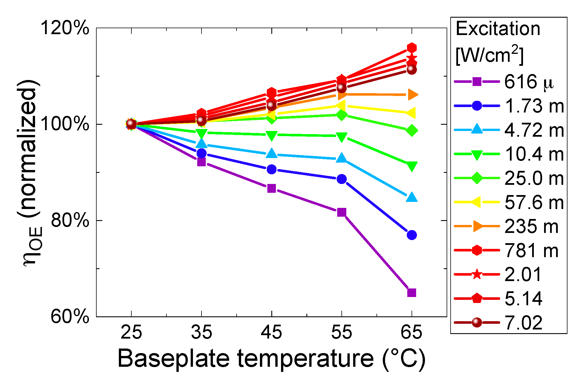
By varying the excitation power, the variation of the (optical-to-electrical) power conversion efficiency was calculated (
Figure 7, where all data were normalized to the value at 25 °C). A decrease in the efficiency is observed with increasing temperature at low excitation densities (up to 10 mW/cm
2); this behavior is ascribed to the fact that, at low excitation densities, non-radiative SRH recombination (whose rate increases with temperature) plays the dominant role. Consequently, carriers can recombine through non-radiative defects before being extracted to generate a photocurrent signal. For higher excitation levels, SRH defects are saturated by a large number of generated carriers, thus defects no longer limit the efficiency of the devices. Power conversion efficiency increases with temperature due to the increased extraction of carriers [
28]: to be extracted from the wells, thus being collected at the contacts, electrons and holes must overcome a potential barrier of 420 meV and 180 meV respectively, assuming a 600 meV In
0.15Ga
0.85n/GaN bandgap discontinuity [
24] with 70:30 ratio between conduction and valence band discontinuities [
29]. This process is enhanced at higher temperatures, leading to an increase in conversion efficiency.
The effects of parasitic series and shunt resistances are limited. Shunt resistance mainly affects
VOC. We observe that the
VOC behavior in
Figure 4b does not fully match the decrease in shunt resistance with increasing excitation power and temperature seen in
Figure 6b. Moreover, the behavior of the short-circuit current (
Figure 5a) cannot be explained by the variation in shunt and series resistance. Thus, there must be other physical phenomena that explain the
JSC and
VOC dependence on the excitation density and on the temperature.
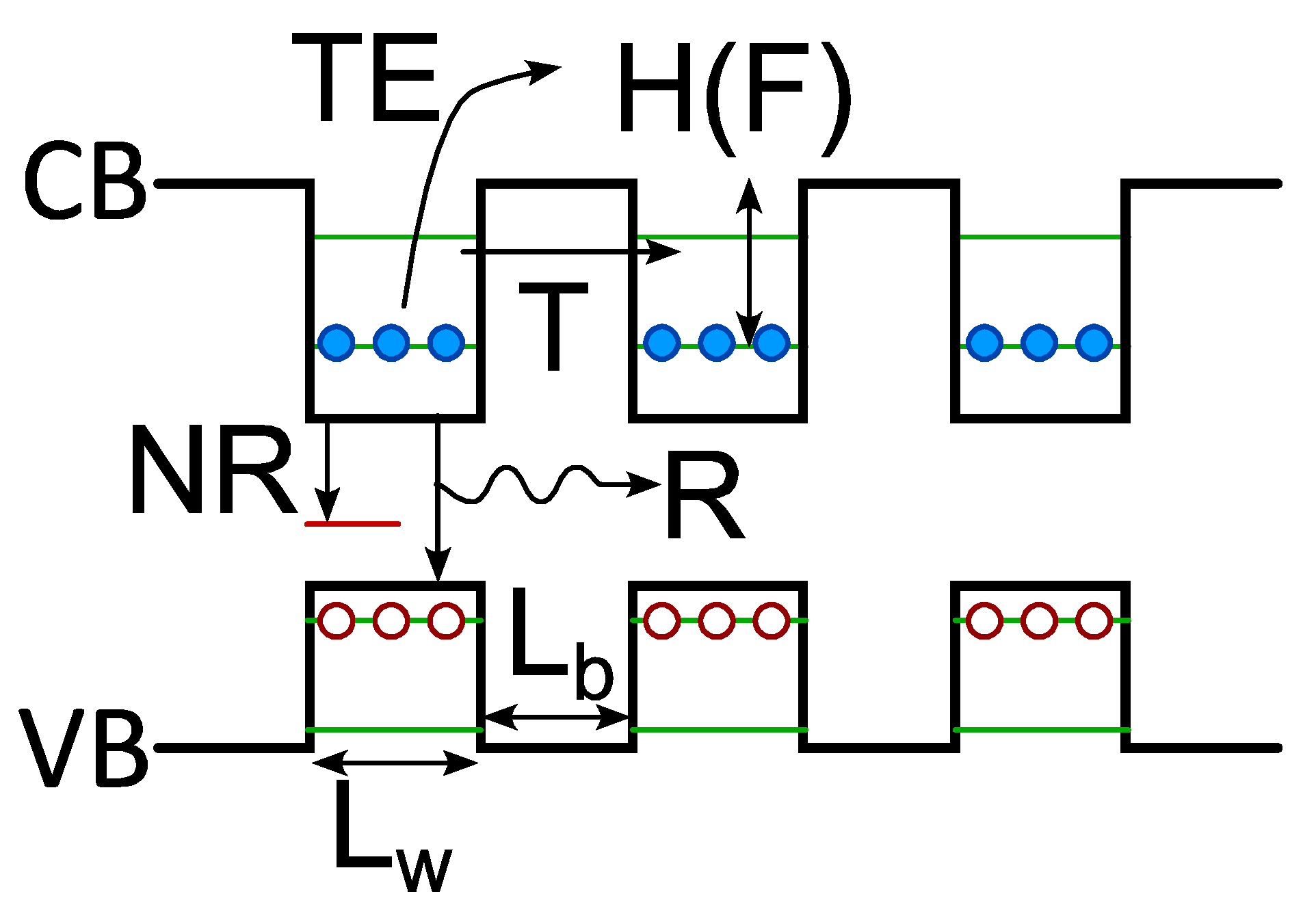
4. Discussion
To fully understand the temperature dependence of the short-circuit current (
Figure 5a) and of the optical-to-electrical power conversion efficiency (
Figure 7) we developed a model based on the physical processes that lead to carrier generation, escape, and recombination, that are schematized in
Figure 8. Because of the nanometric thickness of the well, energy levels inside the wells are quantized. The photogenerated carriers can both recombine radiatively (R) or non radiatively (NR), or can escape from the quantum well by thermionic emission (TE) or tunneling (T) through the GaN barrier [
30].
The total current that is collected from the device is proportional to the sum of the probabilities of single processes, which are proportional to the reciprocal of the lifetime of each mechanism:
There is a minus sign for radiative and non-radiative recombination terms because they prevent photogenerated carriers from escaping from the wells and thus lower short-circuit current.
Analyzing the various contributions to the short-circuit current, the non-radiative recombination is mainly due to SRH recombination, whose rate, assuming the same rate of capture for electrons and holes, is proportional to the number of trap states
NT [
31]:
where
vn is the electron thermal velocity,
σn is the capture cross section of the traps and Δ
E =
ET −
EFi, where
ET is the trap energy level and
EFi is the intrinsic Fermi level energy.
Radiative recombination rate is given by:
where
is the overlap integral between electron and holes,
gred is the reduced density of states and
fc and
fv are the conduction and valence band occupancy, respectively. Usually, this recombination has a lower impact since it is slower than tunneling and thermionic emission [
32], so carriers can easily escape before recombining radiatively.
The tunneling rate can be calculated in the case of a single tunneling barrier. This can be extended to the case of multiple barriers, obtaining [
33]:
where
Lb is the barrier width,
Lw is the well width,
mi is the effective mass in the well,
mb,i is the effective mass in the barrier and
H’i is the field-dependent effective barrier height for tunneling. We can assume that the tunneling rate is not dependent on the intensity, since we are working with similar electric fields. Tunneling is the main escape mechanism in the case of thin barriers [
30].
Thermionic escape current is given by the relation [
34]:
where
nc is the total carrier density in the well and
Hi is the field-dependent effective barrier height for escape. This barrier lowers with increasing intensity, since higher energy levels inside the wells are being occupied by photogenerated carriers.
At temperatures near room temperature, the main process that allows carriers to escape from the wells is tunneling, which can be assumed constant with respect to temperature. By increasing temperature, both SRH recombination and thermionic escape are enhanced; however, thermionic escape is not very effective when excitation density is low and only the first energetic level in the well is occupied, because the effective barrier height is high and thermionic escape rate is limited by the exponential factor in Equation (8). At high intensities,
JSC increases with increasing temperature since thermionic escape becomes more effective due to the increase in thermal energy. This is clearly visible in the normalized short-circuit current in
Figure 5a. To obtain a quantitative estimation of the thermionic escape barrier height, we fitted the experimental short-circuit current at different temperatures with the function:
In this equation, we calculated the short-circuit current as the sum of the three contributions from thermionic escape, SRH recombination and tunneling respectively. We parameterized the unknown variables as intensity-dependent coefficients and we made the temperature dependencies explicit. It is possible to delete the constant by calculating the difference between the short-circuit current at the temperatures
Tk and
T0:
To calculate the values of the parameter A(I) we assumed that, at the three highest excitation densities, only thermionic escape contributes to the JSC variation, since the three normalized curves do not increase further with temperature, possibly due to the fact that SRH recombination is negligible at such high excitation levels and the carriers occupy the highest energy level available in the wells. By fitting the ΔJSC with respect to the temperature with Equation (10) under the constraint B(I) = 0 we obtained ad estimation of A(I) and of the effective barrier height. We then assumed that A(I) has a linear dependence on the excitation density, since it depends on the carrier population inside the wells, and thus we performed a linear fit to have an estimation of its value over the whole excitation range.
We similarly estimated the value of the trap level for SRH recombination by assuming no thermionic escape at the lowest intensity, thus fitting the ΔJSC with the Equation (10) assuming A(I) = 0. From this fit, we estimated a deep level with an energy of 0.33 eV from the midgap. We then repeated this fit for the lowest excitation densities to obtain the value of the coefficient B(I) at the lowest intensities and then we linearly fitted these values to estimate the B(I) coefficient for the whole excitation power range.
Having an estimation of the coefficients
A(
I) and
B(
I) and of the energy of the trap level for SRH recombination, we fitted the Δ
JSC data with Equation (10), leaving
Hi as the fitting parameter. By doing so, we obtained a rough estimation of the effective barrier height, which represents the average effective barrier height for electrons and holes in the 25 quantum wells. From
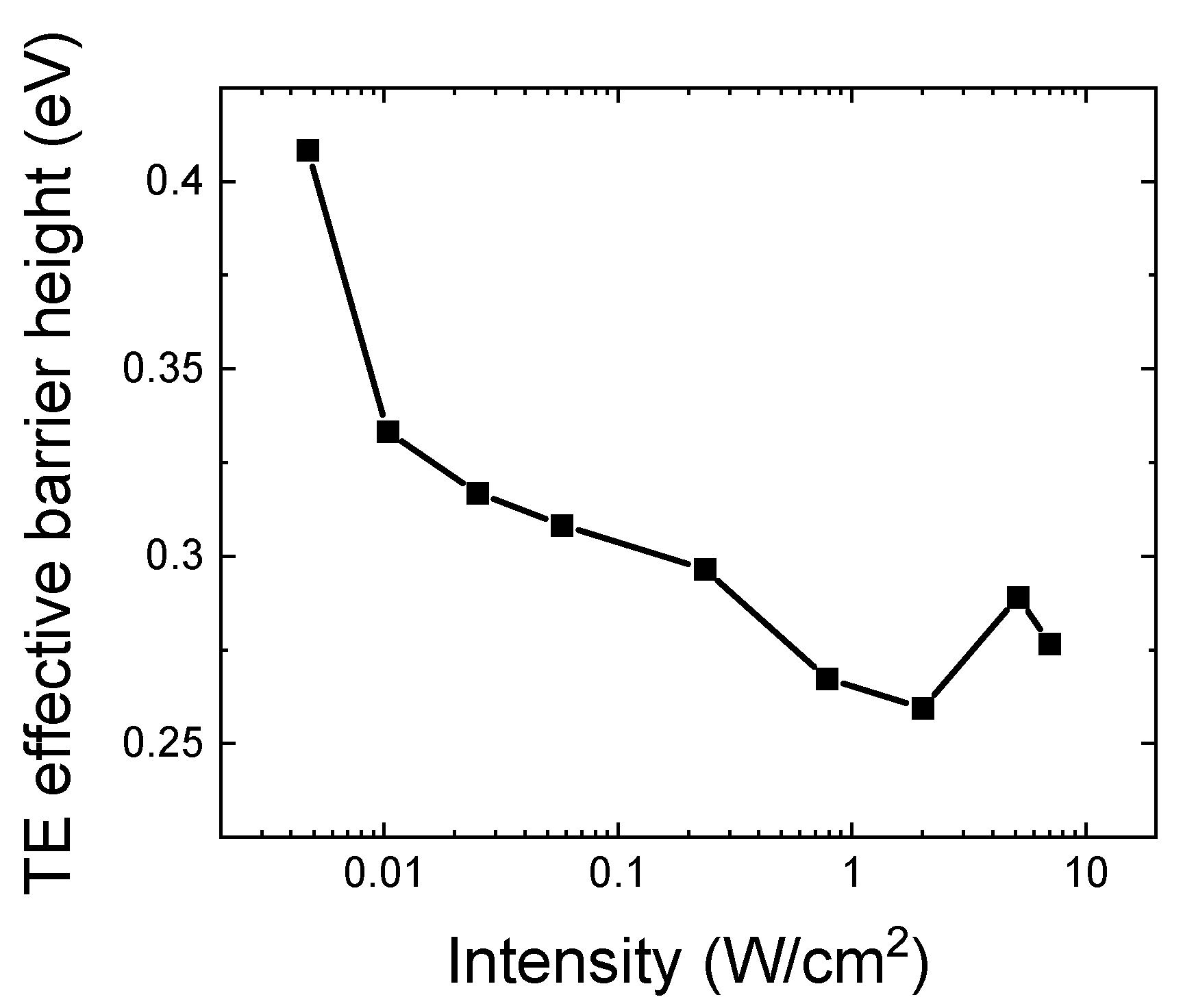
Figure 9 it is possible to see that the effective barrier height needed to fit the experimental data decreases as intensity increases and its values are in agreement with the well depth previously calculated. We thus demonstrated that it is possible to describe the variation in the experimental
JSC data with a model that takes into account SRH recombination and thermionic escape from the wells, the first lowering the short circuit current with increasing temperature, the latter increasing the short-circuit current.
Summarizing, with this model it is possible to account for the efficiency variation seen in the experimental results. SRH recombination effect is clearly seen in the negative temperature coefficient of the short-circuit current (
Figure 5) and of the optical-to-electrical power conversion efficiency (
Figure 7) at low excitation densities: the loss of photogenerated carriers by SRH recombination has a detrimental effect on the device performance, also affecting the
VOC as seen in
Figure 4b. Additionally, EQE (
Figure 2) is measured at low excitation densities, thus its peak lowers with increasing temperature, whilst the absorption by deep levels is enhanced. At higher excitation densities the temperature coefficient becomes positive due to enhanced thermionic emission from wells with a reduced effective barrier height, which effect overcomes the loss of carriers by SRH recombination.
5. Conclusions
In conclusion, we studied InGaN–GaN multiple quantum well photodetectors by analyzing their external quantum efficiency at different wavelengths and extrapolating their main operating parameter under monochromatic excitation at different intensities and temperatures. We found that at low excitation densities short-circuit current, optical-to-electrical conversion efficiency and quantum efficiency decrease with increasing temperature, whereas at high excitation densities, these parameters increase as temperature increases.
This behavior has been attributed to the competition between SRH recombination and thermionic escape from the wells. The first is relevant at low excitation densities and increases with temperature, leading to a decrease in efficiency. The latter is predominant at higher excitation densities, when wells are filled and the effective barrier for thermionic escape is reduced, thus enhancing escape and raising the efficiency.
We developed a model to reproduce the experimental JSC data: the results indicated that the effective barrier height for thermionic escape lowers with increasing excitation density, and allowed us to estimate the position of the defect center responsible for SRH recombination, located far from midgap.

 ,
, 


