Abstract
The present paper focuses on the high-pressure metal-organic vapor phase epitaxy (MOVPE) upside-down vertical reactor (where the inlet of cold gases is below a hot susceptor). This study aims to investigate thermo-kinetic phenomena taking place during the GaN (gallium nitride) growth process using trimethylgallium and ammonia at a pressure of above 2 bar. High pressure accelerates the growth process, but it results in poor thickness and quality in the obtained layers; hence, understanding the factors influencing non-uniformity is crucial. The present investigations have been conducted with the aid of ANSYS Fluent finite volume method commercial software. The obtained results confirm the possibility of increasing the growth rate by more than six times through increasing the pressure from 0.5 bar to 2.5 bar. The analysis shows which zones vortexes form in. Special attention should be paid to the transitional flow within the growth zone as well as the viewport. Furthermore, the normal reactor design cannot be used under the considered conditions, even for the lower pressure value of 0.5 bar, due to high turbulences.
1. Introduction
Metal-Organic Vapor Phase Epitaxy (MOVPE) is one of the most popular deposition methods used in the mass production of compound semiconductors, especially the III–V group compounds, such as gallium nitride (GaN) or gallium arsenide (GaAs). This technique has gained popularity over the past few decades due to rapid amount of development—especially in the field of optoelectronics and power electronic devices—based on these semiconductor materials [1,2,3,4,5,6,7].
The MOVPE process is based on the gas-phase transport of precursors diluted in carrier gases. When reagents are injected into the reactor chamber and flow toward a heated substrate, chemical volumetric reactions occur, resulting in a thin, solid film deposition on the substrate. To ensure the quality and significant purity of the layers obtained during this process, precise equipment and detailed control of the growth parameters are needed. Growth conditions are determined by individual and mutual dependences among the pressure and temperature distributions in the reactor chamber; the type, ratio, and flow rate of the precursors and carrier gasses; as well as some other factors. The process is even more difficult to control if the whole structure—with different layers, various doping, and quantum wells [8,9]—is required, or if selective area growth is considered [10,11,12,13]. Furthermore, the temperature measurements in the reactor chamber are limited due to the restricted access and the expected range (e.g., 600 °C to 1200 °C in the case of GaN). As a consequence, numerical simulations of the process [14,15,16,17,18] are necessary to predict and investigate the growth conditions, and to improve the epitaxy process.
There are several constructions of MOVPE reactors with either lateral or vertical gas flow; among the latter, the inlets can be located above or below a susceptor. In this study, the term normal type is used to refer to the vertical reactor design where gas inlets are located on the top, while the terms inverted or upside-down refer to the designs with inlets placed at the bottom of the chamber.
One of the first comprehensive numerical studies of the MOVPE reactor was presented by Fotiadis et al. [19]. The study focused on a piece of equipment with a vertical design and a susceptor that was 140 mm in diameter; it covered investigations of reactor geometry and operating conditions (i.e., chamber wall temperature, pressure, inlet flow rate, susceptor rotational speed) on heat and mass transfer, as well as uniformity and the rate of the growth process. The conducted analysis showed that the reactor geometry is of crucial importance to the high uniformity of thin-film layer deposition. Subsequent studies focused on specific apparatus constructions from small laboratory size solutions, suitable for processing 3 in wafers [17,20,21,22,23,24,25] up to big, rotating disk or planetary constructions designed for more than 40 2-in substrates [15,26,27,28,29,30]. The researchers investigated the geometry and shape of reactor chambers [15,25,27] with special emphasis placed on the distance between the inlet and the susceptor, the gas injection systems [22,26,31,32] responsible for proper chemical species delivery, as well as the operating parameters of the growth process [15,16,29,33].
Mitrovic et al. [15], as well as Gakis et al. [28], showed that gas flow in MOVPE reactors is driven by injection, rotation, and buoyancy forces. This is especially true of the latter mechanism in the case of normal vertical design, because it acts against injection forces; hence, it can cause vortexes and potentially disturb the laminar character of the flow necessary to properly deliver species to the growth area. To change this situation, the inversion of the reactor can be considered. The numerical studies [19,34] show that the upside-down design can assure an improvement in the film uniformity, although the authors’ investigations were limited to pressure levels of 0.13 and 0.67 bar, respectively. The need for high-pressure growth processes in nowadays GaN device manufacturing is emerging [24].
This study aimed to investigate thermo-fluidic phenomena occurring during the GaN deposition process inside a chamber of a vertical upside-down reactor (where the inlet of cold gases is below a hot susceptor). The motivation for the research was driven by the experimental results of GaN and InGaN (indium gallium nitride) growth under the pressure of more than 2 bar, which proved an increase in the growth rate but presented high non-uniformity and poor quality of the deposited layers. Figure 1 presents the sample results of X-ray powder diffraction (XRD) measurements conducted at five points distributed (at a distance of 1.5 cm) on a sample 2 in wafer. Data analysis allows for the collection of basic information about surface morphology, as gathered below:
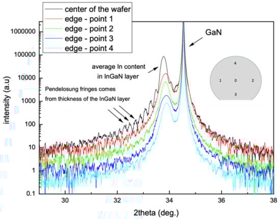
Figure 1.
Results of the XRD (X-ray diffraction) measurements for 5 different points on a sample processed at a pressure of more than 2 bar.
- Point 0 (sample center)—47 nm/13.8% In, good sample quality
- Point 1 (edge)—26 nm/12.7% In, poor sample quality
- Point 2 (edge)—between 25 and 45 nm/12.7% In, poor sample quality
- Point 3 (edge)—28 nm/12.4% In, poor sample quality
- Point 4 (edge)—between 22 and 45 nm/12.2% In, poor sample quality
The center of the wafer exhibits significantly superior quality compared to the edges of the sample. Poor quality, thinner epitaxy layers, and lower indium contents are all indications that non-uniform temperature and flow conditions have occurred.
The novelty of the present paper is in the investigation of upside-down reactors for pressure levels of up to 2.5 bar. The analysis of temperature and flow fields, as well as the growth rate results, allows for the suggestion of changes that can improve the quality of thin-film epitaxy in the high-pressure MOVPE upside-down reactors.
2. Numerical Model
2.1. Reactor Geometry
The geometry of the investigated high-pressure MOVPE upside-down reactor (HP MOVPE) is presented in Figure 2a. The reagents in a gas phase are pumped through the inlet situated at the bottom of the reactor. The gases flow directly into the chamber toward the growth zone, where substrates are attached upside down to the inverted susceptor. The demanded temperature, at a level of 600 °C to 1300 °C at the susceptor, is achieved by heating the coils mounted above it. After the deposition process, unnecessary gasses are pumped out through the gas outlet located on the top of the reactor.
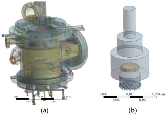
Figure 2.
HP MOVPE (High-Pressure Metal-Organic Vapor Phase Epitaxy) reactor: (a) detailed geometry, (b) simplified 3D geometry.
The detailed geometry of the HP MOVPE reactor was simplified and conformed for numerical analysis purposes. In this step, the reactor model was divided into clear sections without unnecessary components, such as the view window or additional gas inlets (unused in the current setup). A control viewport, situated at the inlet flange, was kept as a possible source of turbulences. The heater was attached to the susceptor to simplify the heat transfer between these two elements. The 3D geometry of the model is shown in Figure 2b. A 2.5 in heater (marked in orange) was attached to a 3 in susceptor (marked in green), within which a special socket for a 2 in substrate is located.
The meshing process resulted in the grid consisting of 1,180,000 elements. Only 20,000 of them covered solid elements, such as the heater, susceptor, and substrates. Special attention was placed on the proper discretization of the growth area. In addition, an inflation algorithm was used, with the first layer’s thickness at 0.1 mm.
2.2. Reaction-Transport Model
Based on our experience [17,35] in MOVPE reactor analysis, a suitable reactor model was prepared. For the numerical investigations presented in the study, ANSYS Fluent was used [36]. Heat and mass transport within the modeled reactor were described with partial differential equations that were determined using mass conservation for every species, momentum conservation, and energy conservation. The model is complemented by a simple kinetic model, presented in [21,22], that covers six volumetric reactions and seven gas–surface reactions that describe GaN growth from trimethylgallium (TMGa) and ammonia (NH3). The properties for the multicomponent ideal gas kinetics and transport were calculated based on [37], after having taken advantage of CHEMKIN libraries. Simulations were conducted with the following assumptions and boundary conditions:
- The inlet fluid is a mixture of the following gases: nitride (N2) as a carrier gas, ammonia (NH3) as an N source in the ratio 3:1, and trimethylgallium (TMGa) as a Ga source (15 µmol/min);
- The reference pressure in the reactor varies from 0.5 bar to 2.5 bar;
- The relative pressure at the outlet equals 0 bar;
- The inlet gas mixture flow rate is 9.5 slm;
- The temperature of the inlet gases equals 22.5 °C;
- The temperature of the reactor walls is 50 °C (cold walls cooled by water);
- The heater temperature equals 850 °C;
- The rotational speed of the susceptor is set to 150 rpm;
- The 2 in sapphire substrate, covered with a 2 µm GaN layer, is placed in a single socket located at the susceptor;
- The Differential Approximation thermal radiation model [36] is used; no heat absorption or scattering within the fluid domain is analyzed; the emissivity value on the chamber walls equals 0.5, while on the susceptor and the substrate this value equals 0.8; the solid surfaces are opaque;
- The SST turbulent model is applied when needed.
3. Results and Discussion
3.1. Thermo-Fluidic Analysis
At first, we have focused on the thermo-fluidic analysis of the upside-down MOVPE reactor under high pressures (0.5 bar and above). Sample results, in the form of the temperature distribution in the reactor cross-section obtained for 0.5 bar pressure inside the tested chamber, are presented in Figure 3. Excess gases exiting the growth area are heated by the heating coil located above the susceptor; therefore, high temperatures (above 200 °C) in the upper section of the reactor can be noticed. A significant temperature gradient in the direction normal to the substrate surface is visible within the growth area. In general, these results conform to the findings of Dilawari and Szekely [34].
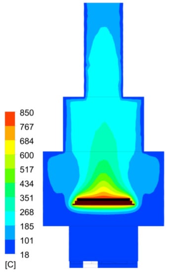
Figure 3.
The temperature distribution in the reactor chamber cross-section, obtained at the pressure of 0.5 bar.
The main difference between the present research and previous studies [15,19,25,28,34] is the place where the constant temperature boundary condition is applied. This location was moved from the susceptor surface to the heater; hence, the resulting temperature distribution on the substrate surface is not constant. Furthermore, it influences the temperature field next to the growth area.
To illustrate this, Figure 4 depicts the temperature variations along the surface diameter of the substrate and the parallel lines located at distances of 100 µm, 200 µm, and 500 µm from it. It can be noted that the temperature field, along the diameter up to the distance of about 2 cm from the center (more than 60% area of the wafer), is homogenous. The temperature decreases ranged from 12 °C at the substrate surface up to 16 °C at a distance of 500 µm from the substrate surface, while moving in the direction of the susceptor edge.
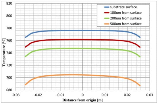
Figure 4.
The temperature distribution along the substrate surface diameter, and at 100 µm, 200 µm, and 500 µm from it, obtained at the pressure of 0.5 bar.
To analyze the gas flow within the chamber, the velocity field was investigated. The sample results of the velocity vector field in the reactor cross-section and the streamlines are illustrated in Figure 5. The flow from the inlet to the growth zone is undisturbed and laminar. This observation is supported by theoretical considerations and the calculations of three numerical criteria, such as Reynolds number (Re), rotational Reynolds number (Reω), and Grashof number (Gr) (which equal 74, 273, and 1.8 × 10⁷, respectively). These values indicate the laminar character of the flow, and their dependences confirm the importance of natural convection in the system. Vortexes form near the reactor walls next to the growth zone, and they might influence the epitaxial process, especially in the areas close to the substrate edges. Gases flowing backward may cause disturbances; they also cool down the susceptor sides, resulting in a non-uniform temperature distribution across the substrate (see Figure 4).
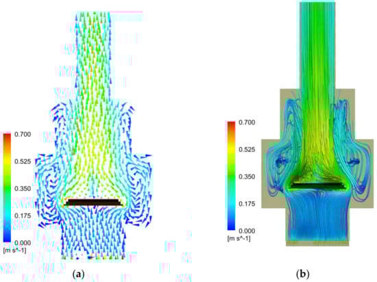
Figure 5.
The velocity field, in the form of (a) vectors and (b) streamlines in the reactor cross-section, obtained at the pressure of 0.5 bar.
Next, the pressure in the chamber was increased from 0.5 bar to 2.5 bar. The sample velocity vectors and streamlines in the cross-section of the modeled structure are presented in Figure 6a,b, respectively. They show that the increase in the pressure within the chamber results in vortexes appearing more frequently in the zone next to the susceptor and above the heater. The presence of the viewport at the inlet flange influences the velocity field within the chamber. Thus, additional carrier gas injection must be considered to compensate for the non-uniformity of gas flow that might result in the formation of eddies. Furthermore, the theoretical considerations and calculations of three numerical criteria have been conducted; Re, Reω, and Gr equal 74, 1364, and 4.5 × 10⁸, respectively. The value of the Grashof number indicates that transitional flow may occur.
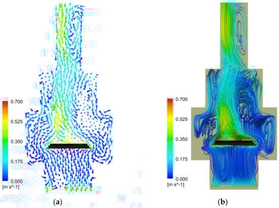
Figure 6.
The velocity field, in the form of (a) vectors and (b) streamlines in the reactor cross-section, obtained at the pressure of 2.5 bar.
To illustrate the differences between the upside-down and normal design for high-pressure processes, the reactor assembly has been inverted back to the normal configuration. In this modification, the gas inlets are located above the susceptor and the gases are injected downward, toward the outlet located at the bottom of the reactor. Free and forced convection, combined in the flow, act against each other. The velocity vectors and streamlines for the normal vertical reactor are presented in Figure 7. Sample results, calculated at the pressure of 0.5 bar inside the reactor chamber, show eddies within the growth zone. These results are consistent with previous studies [25,33].
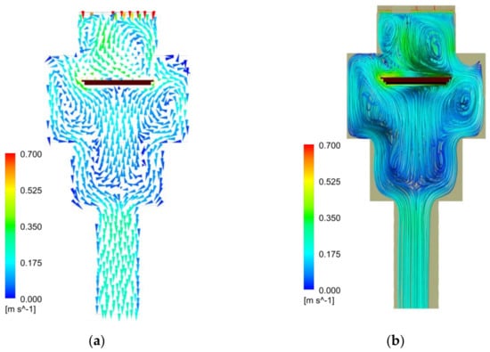
Figure 7.
The velocity field in the vertical, normal MOVPE (Metal-Organic Vapor Phase Epitaxy) reactor cross-section, in the form of (a) vectors and (b) streamlines, obtained at the pressure of 0.5 bar.
Figure 8 depicts the comparison of the temperature distributions along the diameter of the substrate, which accounts for two different pressure values and includes both the upside-down and the normal designs. The presented characteristics show that, in the case of the inverted reactor, the increase in the pressure from 0.5 bar to 2.5 bar results in a temperature drop of 4 °C in the center area of the substrate, with slight temperature profile changes moving toward the wafer edge (i.e., more intensive cooling of the susceptor). The uniformity of the temperature distributions across the substrate is comparable. Temperatures of 774 ± 1 °C and 770 ± 1 °C are obtained from the substrate area, with diameters of 1.85 cm and 1.4 cm for the pressure levels of 0.5 bar and 2.5 bar, respectively. Conversely, the temperature field for the normal configuration is uneven, which is in agreement with the velocity field presented in Figure 7.
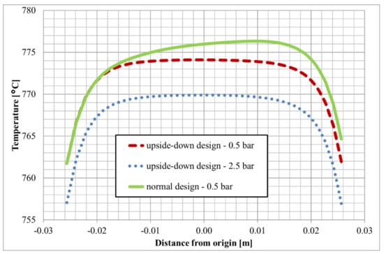
Figure 8.
The temperature distribution along the substrate surface diameter for the upside-down and normal designs, at pressure levels of 0.5 bar and 2.5 bar.
3.2. Growth Rate
The thin-film epitaxy process, and the quality of the obtained layers, are strongly influenced by the temperature and velocity fields discussed in Section 3.1. Laminar flow and the required temperature distributions are necessary conditions, but they may not be sufficient alone. To analyze this, the results, in the form of the GaN growth rates obtained at pressure levels of 0.5 and 2.5 bar in the upside-down and normal reactors, are depicted in Figure 9 and Figure 10. Figure 9 presents the GaN deposition rate in the form of color maps, while Figure 10 shows the changes in the quantity along the diameters for the three analyzed cases. These characteristics are obtained as a result of the averaging process of the values along the substrate’s horizontal and vertical diameters.
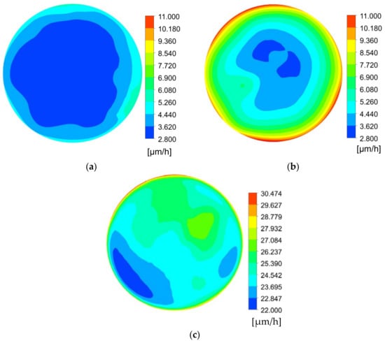
Figure 9.
GaN (gallium nitride) growth rates obtained from (a) the upside-down reactor at 0.5 bar, (b) the normal reactor at 0.5 bar, and (c) the upside-down reactor at 2.5 bar.
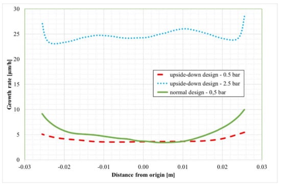
Figure 10.
The GaN (gallium nitride) growth rate distribution along the wafer diameter for the three analyzed cases.
The calculated growth rate depends on the pressure. The average deposition rate equals 3.9 µm/h and 5.1 µm/h at 0.5 bar for the inverted and normal design, respectively; however, it reaches 24.6 µm/h at 2.5 bar in the upside-down reactor. When considering the lower value of the investigated pressure (see Figure 9a,b), the upside-down design results in better uniformity of GaN layer thickness (i.e., growth rate deviation of ± 0.5 µm/h for the whole wafer, lowered below ± 0.1 µm/h while considering an area with a 4 cm diameter), which is in agreement with the conclusions that were drawn based on the velocity field analysis (see Section 3.1, Figure 5 and Figure 7). In the inverted reactor, due to pressure increase, the epitaxy process can be shortened more than six times; however, the growth rate deviation exceeds ± 3 µm/h. Moreover, the color map presented in Figure 9c illustrates the influence of the viewport that disturbs the flow (see Figure 6).
4. Conclusions
The present research has focused on the analysis of thermal-kinetic phenomena, as well as the growth rate of the GaN layer from TMGa and ammonia with nitrogen as a carrier gas, in the high-pressure MOCVD upside-down reactor. The authors mainly focus on comparative analyses between the pressure of 0.5 bar and 2.5 bar and the normal and converted vertical reactor designs. It has been shown that at the pressure of 2.5 bar in the chamber, the growth rate can be highly accelerated. Even though the obtained results show uniform temperature distribution, the velocity field and the modeled growth rate depict non-uniformity in the layer thickness. Furthermore, the temperature drops closer to the edges of the substrate surface. The values exceed 10 °C in numerical simulations at both 0.5 bar and 2.5 bar in the upside-down reactor. This is even more important when considering the simplification that is introduced to the model in the form of physical contact between the heater and the susceptor. In the real reactor, the situation could be even worse, which can have a big impact on the deposition process in this area. Moreover, eddies form along the sidewalls of the chamber next to the susceptor sides. The vortexes cool the susceptor; hence, they affect the temperature distribution within the growth zone. To benefit from the upside-down design, further investigation of vortex reduction is necessary so that better temperature and precursor delivery uniformity—and, hence, the deposition process quality—can be ensured.
Author Contributions
Conceptualization, M.L., J.P., and R.C.; methodology, P.N. and E.R.; software, P.N.; validation, E.G., R.C., J.P., and P.N.; investigation, P.N.; resources, P.N. and E.R.; data curation, P.N.; writing—original draft preparation, P.N.; writing—review and editing, E.R.; visualization, P.N.; supervision, E.R. and Z.L. All authors have read and agreed to the published version of the manuscript.
Funding
This research received no external funding.
Conflicts of Interest
The authors declare no conflict of interest.
References
- Wasisto, H.S.; Prades, J.D.; Gülink, J.; Waag, A. Beyond solid-state lighting: Miniaturization, hybrid integration, and applications of GaN nano-and micro-LEDs. Appl. Phys. Rev. 2019, 6. [Google Scholar] [CrossRef] [Green Version]
- Leszczynski, M.; Grzanka, E.; Czernecki, R.; Perlin, P. Material Issues in GaN-based Laser Diode Manufacturing. In Proceedings of the 2019 Conference on Lasers and Electro-Optics (CLEO), San Jose, CA, USA, 5–10 May 2019; pp. 12–13. [Google Scholar] [CrossRef]
- Rodríguez-Benítez, O.M.; Ponce-Silva, M.; Aquí-Tapia, J.A.; Claudio-Sánchez, A.; Vela-Váldes, L.G.; Lozoya-Ponce, R.E.; Cortés-García, C. Comparative performance and assessment study of a current-fed dc-dc resonant converter combining si, sic, and gan-based power semiconductor devices. Electronics 2020, 9, 1982. [Google Scholar] [CrossRef]
- Ballestín-Fuertes, J.; Muñoz-Cruzado-alba, J.; Sanz-Osorio, J.F.; Laporta-Puyal, E. Role of wide bandgap materials in power electronics for smart grids applications. Electronics 2021, 10, 677. [Google Scholar] [CrossRef]
- Hartmann, J.; Manglano Clavero, I.; Nicolai, L.; Margenfeld, C.; Spende, H.; Ledig, J.; Zhou, H.; Steib, F.; Jaros, A.; Avramescu, A.; et al. 3D GaN Fins as a Versatile Platform for a-Plane-Based Devices. Phys. Status Solidi Basic Res. 2019, 256, 1–9. [Google Scholar] [CrossRef] [Green Version]
- Wang, X.; Peng, W.; Yu, R.; Zou, H.; Dai, Y.; Zi, Y.; Wu, C.; Li, S.; Wang, Z.L. Simultaneously Enhancing Light Emission and Suppressing Efficiency Droop in GaN Microwire-Based Ultraviolet Light-Emitting Diode by the Piezo-Phototronic Effect. Nano Lett. 2017, 17, 3718–3724. [Google Scholar] [CrossRef] [PubMed]
- Hou, S.H.Z.; Iu, X.I.L.; An, H.A.N.Y.; Hen, Z.H.C.; Iu, Y.I.L.; Iu, S.H.L. Highly efficient GaN-based high-power flip- chip light-emitting diodes. Opt. Express 2019, 27, 669–692. [Google Scholar]
- Sarzyński, M.; Grzanka, E.; Grzanka, S.; Targowski, G.; Czernecki, R.; Reszka, A.; Holy, V.; Nitta, S.; Liu, Z.; Amano, H.; et al. Indium incorporation into InGaN quantum wells grown on GaN narrow stripes. Materials 2019, 12, 2583. [Google Scholar] [CrossRef] [PubMed] [Green Version]
- Watson, I.M. Metal organic vapour phase epitaxy of AlN, GaN, InN and their alloys: A key chemical technology for advanced device applications. Coord. Chem. Rev. 2013, 257, 2120–2141. [Google Scholar] [CrossRef]
- Waag, A.; Wang, X.; Fündling, S.; Ledig, J.; Erenburg, M.; Neumann, R.; Al Suleiman, M.; Merzsch, S.; Wei, J.; Li, S.; et al. The nanorod approach: GaN NanoLEDs for solid state lighting. Phys. Status Solidi Curr. Top. Solid State Phys. 2011, 8, 2296–2301. [Google Scholar] [CrossRef]
- Coltrin, M.E.; Mitchell, C.C. Mass transport and kinetic limitations in MOCVD selective-area growth. J. Cryst. Growth 2003, 254, 35–45. [Google Scholar] [CrossRef]
- Stępniak, M.; Wośko, M.; Prażmowska-Czajka, J.; Stafiniak, A.; Przybylski, D.; Paszkiewicz, R. Growth uniformity in selective area epitaxy of algan/gan heterostructures for the application in semiconductor devices. Electronics 2020, 9, 2129. [Google Scholar] [CrossRef]
- Roshko, A.; Brubaker, M.; Blanchard, P.; Harvey, T.; Bertness, K.A. Selective area growth and structural characterization of GaN nanostructures on si(111) substrates. Crystals 2018, 8, 366. [Google Scholar] [CrossRef] [Green Version]
- Mitrovic, B.; Parekh, A.; Ramer, J.; Merai, V.; Armour, E.A.; Kadinski, L.; Gurary, A. Reactor design optimization based on 3D modeling of nitrides deposition in MOCVD vertical rotating disc reactors. J. Cryst. Growth 2006, 289, 708–714. [Google Scholar] [CrossRef]
- Mitrovic, B.; Gurary, A.; Quinn, W. Process conditions optimization for the maximum deposition rate and uniformity in vertical rotating disc MOCVD reactors based on CFD modeling. J. Cryst. Growth 2007, 303, 323–329. [Google Scholar] [CrossRef]
- Fang, H.; Zhang, Z.; Pan, Y.; Ma, R.; Liu, S.; Wang, M. Systematic study of epitaxy growth uniformity in a specific MOCVD reactor. Cryst. Res. Technol. 2014, 49, 907–918. [Google Scholar] [CrossRef]
- Raj, E.; Lisik, Z.; Niedzielski, P.; Ruta, L.; Turczynski, M.; Wang, X.; Waag, A. Modelling of MOCVD reactor: New 3D approach. J. Phys. Conf. Ser. 2014, 494, 012019. [Google Scholar] [CrossRef] [Green Version]
- Saskia, S.; Tomida, D.; Ishiguro, T.; Honda, Y.; Chichibu, S.; Amano, H. Numerical Simulation of Ammonothermal Crystal Growth of. Crystals 2021, 11, 356. [Google Scholar]
- Fotiadis, D.I.; Kieda, S.; Jensen, K.F. Transport phenomena in vertical reactors for metalorganic vapor phase epitaxy. I. Effects of heat transfer characteristics, reactor geometry, and operating conditions. J. Cryst. Growth 1990, 102, 441–470. [Google Scholar] [CrossRef]
- Zhong, S.Q.; Ren, X.M.; Huang, Y.Q.; Wang, Q.; Huang, H. Numerical studies on flow and thermal fields in MOCVD reactor. Chin. Sci. Bull. 2010, 55, 560–566. [Google Scholar] [CrossRef]
- Pawlowski, R.P.; Theodoropoulos, C.; Salinger, A.G.; Mountziaris, T.J.; Moffat, H.K.; Shadid, J.N.; Thrush, E.J. Fundamental models of the metalorganic vapor-phase epitaxy of gallium nitride and their use in reactor design. J. Cryst. Growth 2000, 221, 622–628. [Google Scholar] [CrossRef]
- Theodoropoulos, C.; Mountziaris, T.J.; Moffat, H.K.; Han, J. Design of gas inlets for the growth of gallium nitride by metalorganic vapor phase epitaxy. J. Cryst. Growth 2000, 217, 65–81. [Google Scholar] [CrossRef]
- Sun, J.; Redwing, J.M.; Kuech, T.F. Model development of GaN MOVPE growth chemistry for reactor design. J. Electron. Mater. 2000, 29, 2–9. [Google Scholar] [CrossRef]
- Martin, C.; Dauelsberg, M.; Protzmann, H.; Boyd, A.R.; Thrush, E.J.; Heuken, M.; Talalaev, R.A.; Yakovlev, E.V.; Kondratyev, A.V. Modelling of group-III nitride MOVPE in the closed coupled showerhead reactor and Planetary Reactor®. J. Cryst. Growth 2007, 303, 318–322. [Google Scholar] [CrossRef]
- Tseng, C.F.; Tsai, T.Y.; Huang, Y.H.; Lee, M.T.; Horng, R.H. Transport phenomena and the effects of reactor geometry for epitaxial GaN growth in a vertical MOCVD reactor. J. Cryst. Growth 2015, 432, 54–63. [Google Scholar] [CrossRef]
- Kadinski, L.; Merai, V.; Parekh, A.; Ramer, J.; Armour, E.A.; Stall, R.; Gurary, A.; Galyukov, A.; Makarov, Y. Computational analysis of GaN/InGaN deposition in MOCVD vertical rotating disk reactors. J. Cryst. Growth 2004, 261, 175–181. [Google Scholar] [CrossRef]
- Parikh, R.P.; Adomaitis, R.A. An overview of gallium nitride growth chemistry and its effect on reactor design: Application to a planetary radial-flow CVD system. J. Cryst. Growth 2006, 286, 259–278. [Google Scholar] [CrossRef]
- Gakis, G.P.; Koronaki, E.D.; Boudouvis, A.G. Numerical investigation of multiple stationary and time-periodic flow regimes in vertical rotating disc CVD reactors. J. Cryst. Growth 2015, 432, 152–159. [Google Scholar] [CrossRef]
- Zheng, J.; Fang, H.; Zhang, Z.; Yang, J.; Gan, Z.; Yan, H. Uniformity analysis of temperature distribution in an industrial MOCVD reactor. Cryst. Res. Technol. 2016, 51, 617–626. [Google Scholar] [CrossRef]
- Li, J.; Fei, Z.Y.; Xu, Y.F.; Wang, J.; Fan, B.F.; Ma, X.J.; Wang, G. Study on the optimization of the deposition rate of planetary GAN-MOCVD films based on CFD simulation and the corresponding surface model. R. Soc. Open Sci. 2018, 5. [Google Scholar] [CrossRef] [Green Version]
- Li, J.; Wang, J.; Cai, J.D.; Xu, Y.F.; Fan, B.F.; Wang, G. Numerical simulation and analysis of process parameters of GaN-MOCVD reactor. Int. Commun. Heat Mass Transf. 2018, 91, 64–76. [Google Scholar] [CrossRef]
- Shin, C.Y.; Baek, B.J.; Lee, C.R.; Pak, B.; Yoon, J.M.; Park, K.S. Numerical analysis for the growth of GaN layer in MOCVD reactor. J. Cryst. Growth 2003, 247, 301–312. [Google Scholar] [CrossRef]
- Mitrovic, B.; Gurary, A.; Kadinski, L. On the flow stability in vertical rotating disc MOCVD reactors under a wide range of process parameters. J. Cryst. Growth 2006, 287, 656–663. [Google Scholar] [CrossRef]
- Dilawari, A.H.; Szekely, J. A mathematical representation of a modified stagnation flow reactor for MOCVD applications. J. Cryst. Growth 1991, 108, 491–498. [Google Scholar] [CrossRef]
- Niedzielski, P. Comparison of trimethylgallium decomposition models for epitaxy growth analysis in MOVPE reactors. J. Phys. Conf. Ser. 2020, 1534. [Google Scholar] [CrossRef]
- ANSYS Inc. ANSYS Fluent Theory Guide; ANSYS Inc.: Canonsburg, PA, USA, 2015. [Google Scholar]
- Hellman, E.S. Internet Journal Nitride Semiconductor Research. Mater. Res. 1999, 2, 1–10. [Google Scholar]
Publisher’s Note: MDPI stays neutral with regard to jurisdictional claims in published maps and institutional affiliations. |
© 2021 by the authors. Licensee MDPI, Basel, Switzerland. This article is an open access article distributed under the terms and conditions of the Creative Commons Attribution (CC BY) license (https://creativecommons.org/licenses/by/4.0/).