High Speed Back-Bias Voltage (VBB) Generator with Improved Pumping Current

Abstract
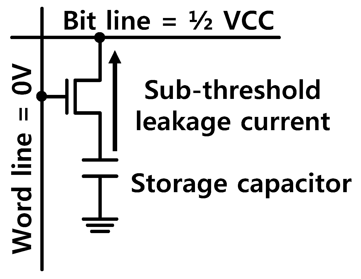
:1. Introduction
2. Conventional VBB Generation Circuits
2.1. Conventional Cross-Coupled Hybrid Pumping Circuit (Conv 1)
2.2. Conventional Cross-Coupled Hybrid Pumping Circuit (Conv 2)
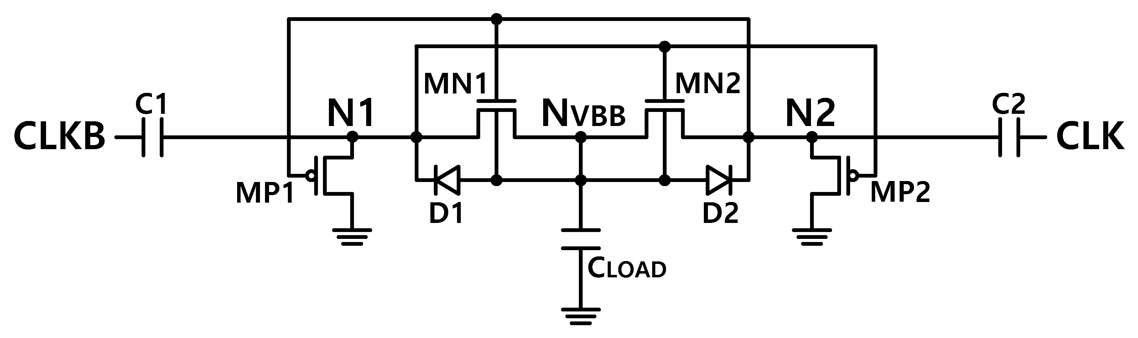
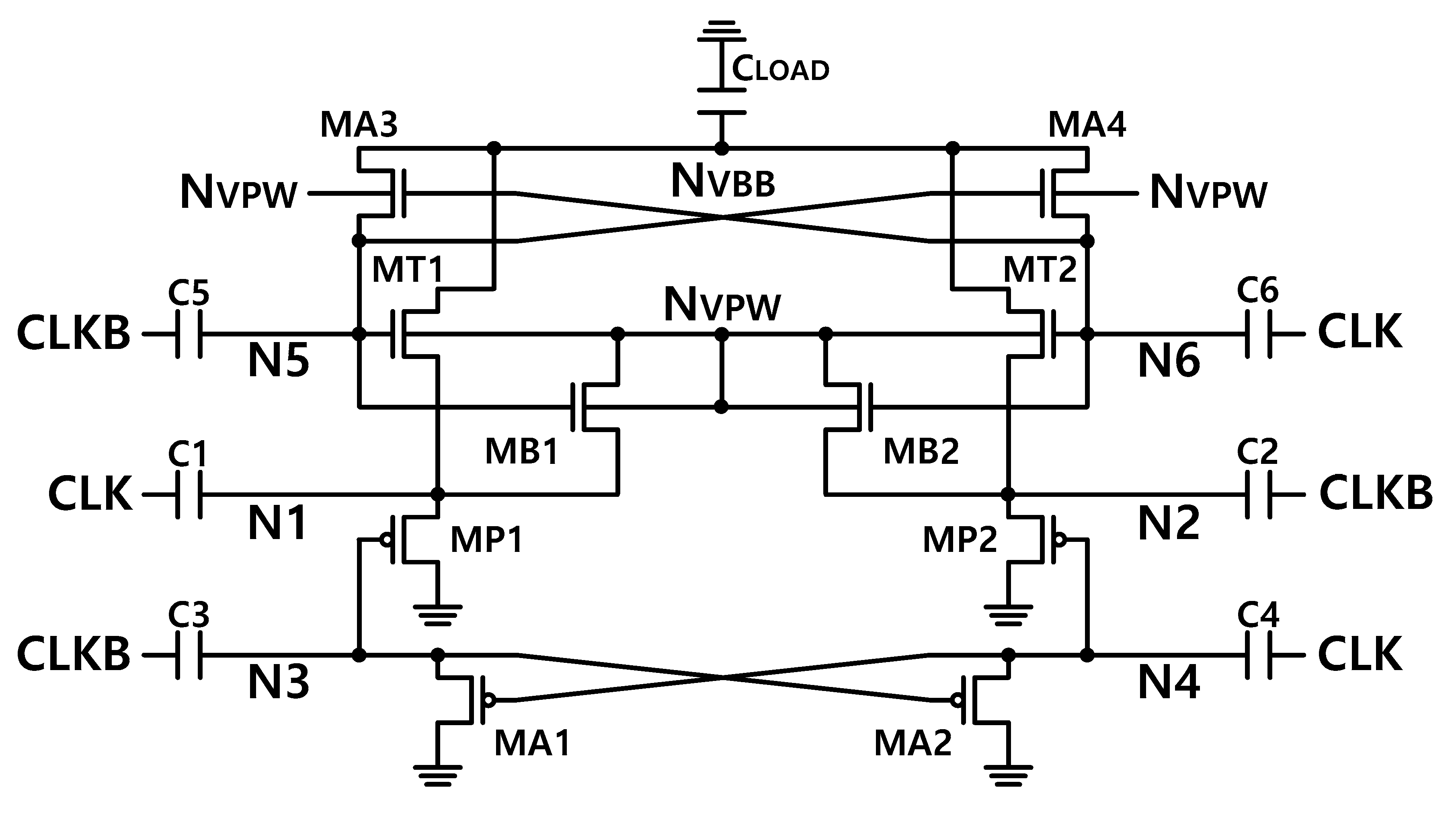
2.3. Conventional Cross-Coupled Hybrid Pumping Circuit Using the Auxiliary Pump (Conv 3)
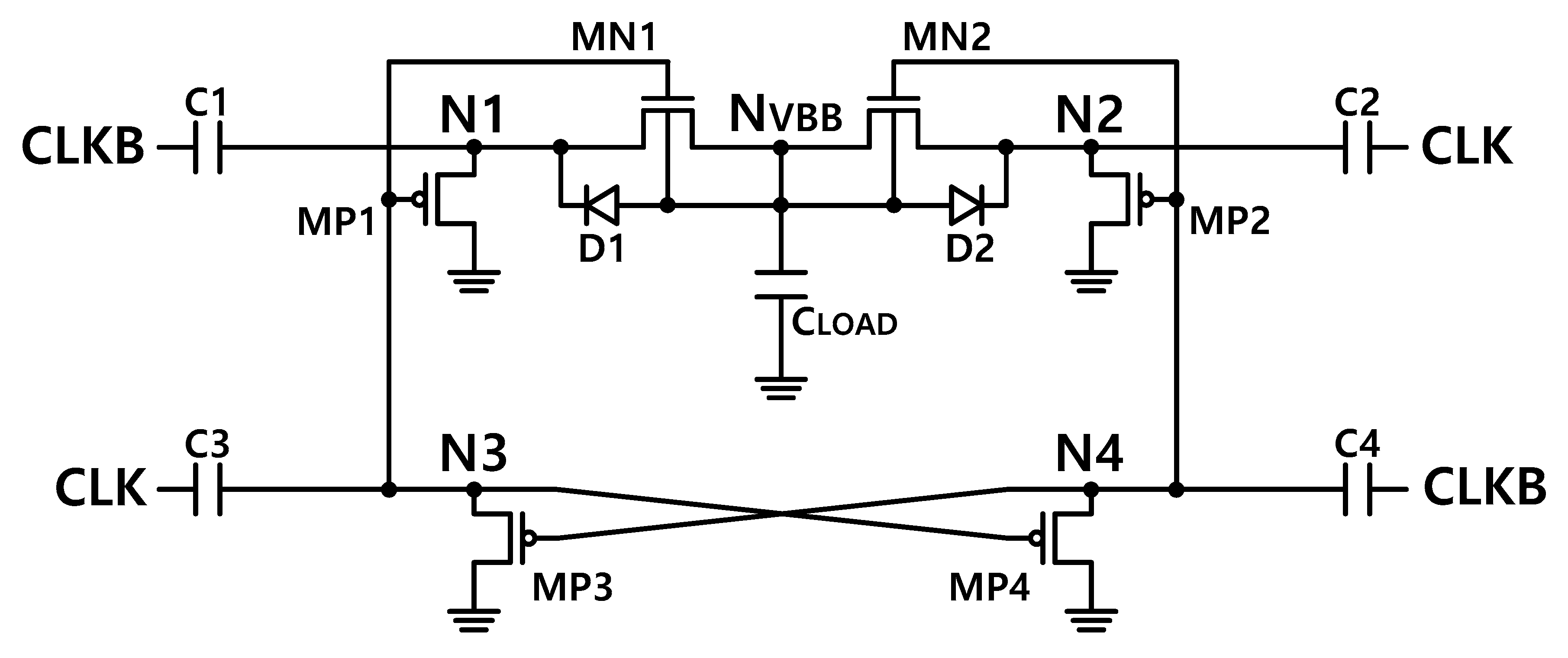
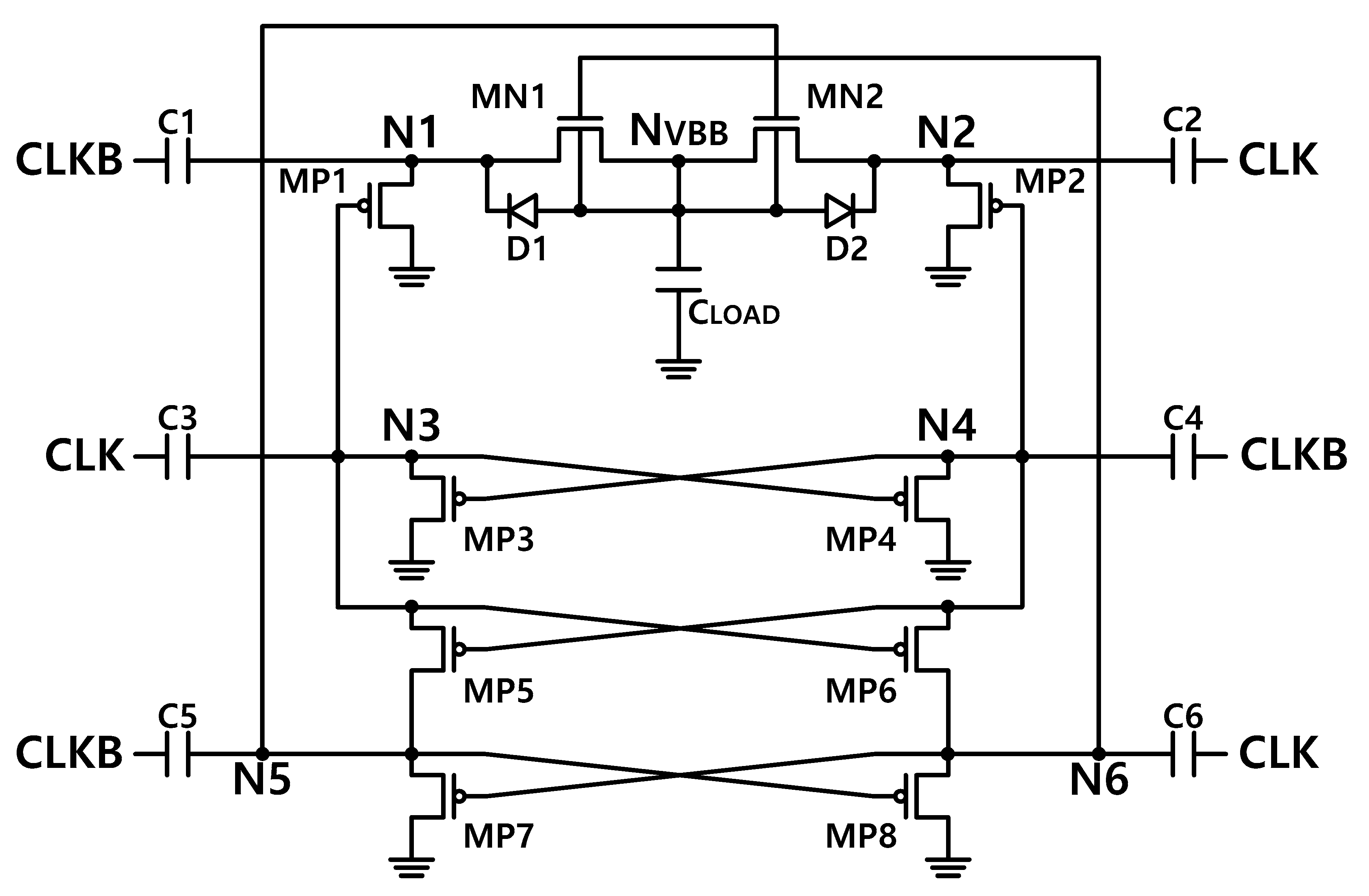
3. Proposed Cross-Coupled Hybrid Pumping Circuit
4. Experiment Results
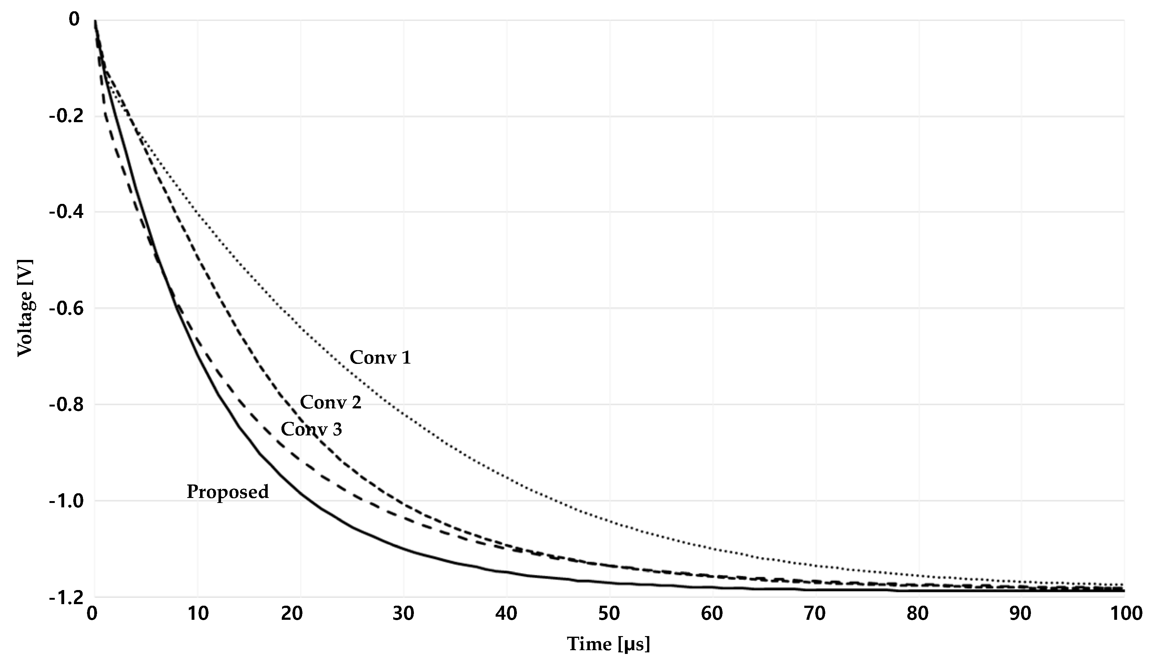
4.1. Pump-Down Speed
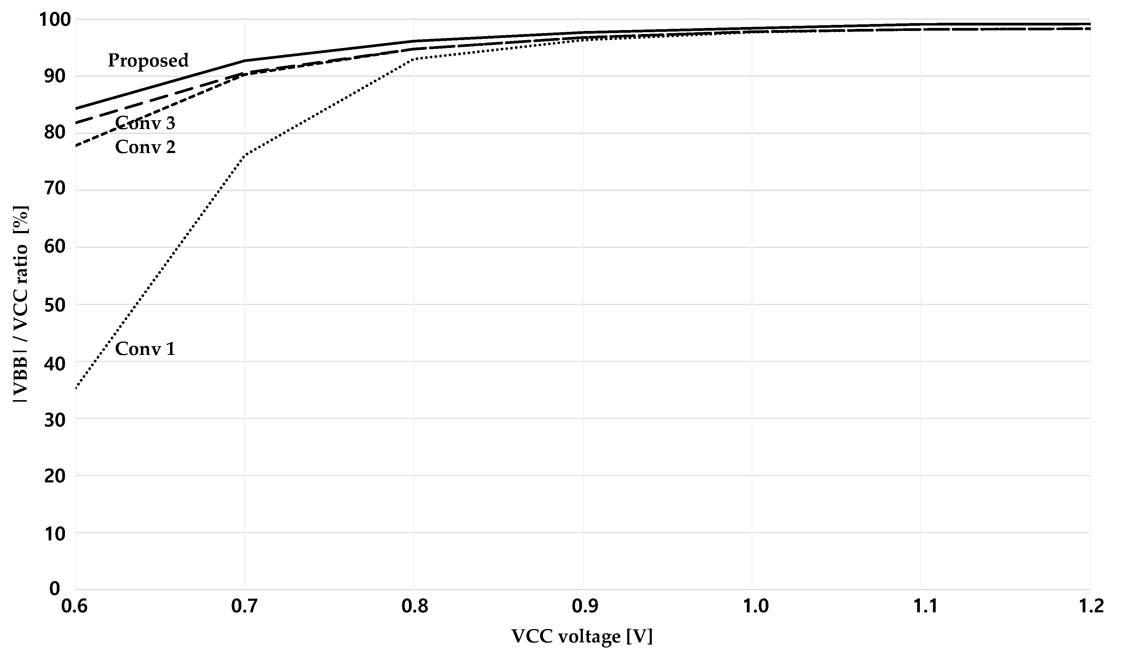
4.2. |VBB|/VCC
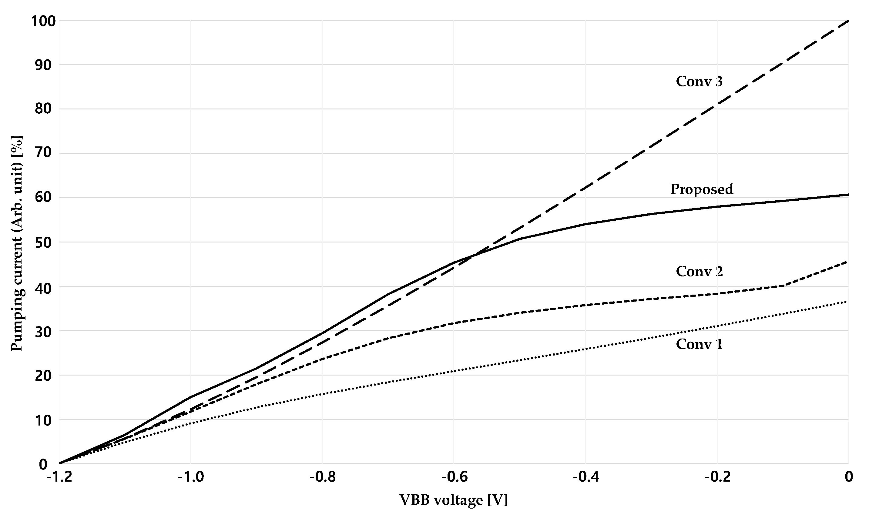
4.3. Pumping Current
5. Conclusions
Author Contributions
Funding
Acknowledgments
Conflicts of Interest
References
- Nakagome, Y.; Kawamoto, Y.; Tanaka, H.; Takeuchi, K.; Kume, E.; Watanabe, Y.; Kaga, T.; Murai, F.; Izawa, R.; Hisamoto, D.; et al. A 1.5 V circuit technology for 64 Mb DRAMs. In Proceedings of the Digest of Technical Papers, 1990 Symposium on VLSI Circuits, Honolulu, HI, USA, 7–9 June 1990; pp. 17–18. [Google Scholar]
- Min, K.S.; Jin, K.W.; Kim, J.B. A high-efficiency back-bias generator with cross-coupled hybrid pumping circuit for sub-1.5 v DRAM applications. In Proceedings of the European Soli-state Circuits and Devices Conference, Stockholm, Sweden, 19–21 September 2000. [Google Scholar]
- Tsukikawa, Y.; Okasaka, Y.; Furutani, K.; Kajimoto, T.; Morooka, Y.; Miyamoto, H.; Ozaki, H. An efficient back-bias generator with hybrid pumping circuit for 1.5-V DRAMs. IEEE J. Solid State Circuits 1994, 29, 534–538. [Google Scholar] [CrossRef]
- Kim, Y.-H.; Sim, J.-Y.; Park, H.-J.; Doh, J.-I.; Park, K.-W.; Chung, H.-W.; Oh, J.-H.; Oh, C.-S.; Ahn, S.-H. Analysis and prevention of DRAM latch-up during power-on. IEEE J. Solid State Circuits 1997, 32, 79–85. [Google Scholar] [CrossRef]
- Min, K.S.; Chung, J.Y. A fast pump-down VBB generator for sub-1.5-V DRAMs. JSSC 2001, 36, 1154–1157. [Google Scholar]
- Takashima, D.; Watanabe, S.; Nakano, H.; Oowaki, Y.; Ohuchi, K.; Tango, H. Standby/active mode logic for sub-1-V operating ULSI memory. IEEE J. Solid State Circuits 1994, 29, 441–447. [Google Scholar] [CrossRef]
- Min, K.-S.; Kim, Y.-H.; Kim, D.; Kim, D.M.; Cho, S.-I.; Ahn, J.-H.; Chung, J.-Y. An 80% larger-current-output negative CMOS charge pump with 10% area penalty for sub-1-V-VCC negative-word-line DRAMs. Curr. Appl. Phys. 2003, 3, 507–510. [Google Scholar] [CrossRef]
- Sato, K.; Kawamoto, H.; Yanagisawa, K.; Matsumoto, T.; Shimizu, S.; Hori, R. 20NS Static column 1mb dram in CMOS technology. In Proceedings of the international Solid-State Circuits Conference, New York, NY, USA, 13–15 February 1985. [Google Scholar]
- Kim, Y.H.; Park, H.J.; Sohn, J.D.; Choi, J.S.; Park, C.S.; Ahn, S.H.; Jeong, J.Y. Two-phase back-bias generator for low-voltage gigabit DRAMs. Electron. Lett. 1998, 34, 1831–1833. [Google Scholar] [CrossRef]
- Cho, T.B.; Gray, P.R. A 10-bit, 20-MS/s, 35-mW pipeline A/D converter. In Proceedings of the IEEE Custom Integrated Circuits Conference CICC’94, San Diego, CA, USA, 1–4 May 1994. [Google Scholar]
- Favrat, P.; Deval, P.; Declercq, M.J. A high-efficiency CMOS voltage doubler. IEEE J. Solid State Circuits 1998, 33, 410–416. [Google Scholar] [CrossRef]


| Phase | CLK | CLKB | MP1 | MP2 | MN1 | MN2 | VN1 | VN2 |
|---|---|---|---|---|---|---|---|---|
| 1 | High | Low | Off | On | On | Off | 0 | VCC |
| |Vtp| | ||||||||
| 2 | Low | High | On | Off | Off | On | VCC | |Vtp|−VCC |
| 0 | ||||||||
| 3 | High | Low | Off | On | On | Off | −VCC | |Vtp| |
| 0 | ||||||||
| 4 | Low | High | On | Off | Off | On | 0 | −VCC |
| 5 | High | Low | Off | On | On | Off | −VCC | 0 |
| Phase | CLK | MP1 | MP3 | MN1 | VN1 | VN2 | VN3 | VN4 |
|---|---|---|---|---|---|---|---|---|
| 1 | High | Off | On | On | 0 | VCC | VCC | 0 |
| |Vtp| | |Vtp| | |||||||
| 2 | Low | On | Off | Off | VCC | |Vtp|−VCC | |Vtp|−VCC | VCC |
| 0 | 0 | |||||||
| 3 | High | Off | On | On | −VCC | |Vtp| | |Vtp| | −VCC |
| 0 | 0 | |||||||
| 4 | Low | On | Off | Off | 0 | −VCC | −VCC | 0 |
| 5 | High | Off | On | On | −VCC | 0 | 0 | −VCC |
| Phase | CLK | MA1 | MP1 | MT1 | VN1 | VN2 | VN3 | VN4 | VNVPW |
|---|---|---|---|---|---|---|---|---|---|
| 1 | High | Off | On | On | VCC | 0 | 0 | 0 | 0 |
| |Vtp| | |Vtp| | ||||||||
| 2 | Low | On | Off | Off | |Vtp|−VCC | VCC | VCC | |Vtp|−VCC | |Vtp|−VCC |
| 0 | 0 | ||||||||
| 3 | High | Off | On | On | |Vtp| | −VCC | −VCC | |Vtp| | −VCC |
| 0 | 0 | ||||||||
| 4 | Low | On | Off | Off | −VCC | 0 | 0 | −VCC | −VCC |
| 5 | High | Off | On | On | 0 | −VCC | −VCC | 0 | −VCC |
| Phase | CLK | MP1 | MP3 | MP5 | MP7 | MN1 | VN1 | VN2 | VN3 | VN4 | VN5 | VN6 |
|---|---|---|---|---|---|---|---|---|---|---|---|---|
| 1 | High | Off | On | On | Off | On | 0 | VCC | VCC | 0 | 0 | VCC |
| |Vtp| | |Vtp| | A | |Vtp| | |||||||||
| 2 | Low | On | Off | Off | On | Off | VCC | |Vtp|−VCC | |Vtp|−VCC | VCC | A + VCC | |Vtp|−VCC |
| 0 | |Vtp|−VCC + B | −C | A + VCC−B | |Vtp|−VCC + C | ||||||||
| 3 | High | Off | On | On | Off | On | −VCC | |Vtp| | |Vtp| +B | −C−VCC | A−B | |Vtp| + C |
| 0 | −C | |||||||||||
| 4 | Low | On | Off | Off | On | Off | 0 | −VCC | −C−VCC | −C | A−B + VCC | |Vtp|−VCC + C |
| 5 | High | Off | On | On | Off | On | −VCC | 0 | −C | −C−VCC | A−B | |Vtp| + C |
Publisher’s Note: MDPI stays neutral with regard to jurisdictional claims in published maps and institutional affiliations. |
© 2020 by the authors. Licensee MDPI, Basel, Switzerland. This article is an open access article distributed under the terms and conditions of the Creative Commons Attribution (CC BY) license (http://creativecommons.org/licenses/by/4.0/).
Share and Cite
Yim, T.; Lee, C.; Yoon, H. High Speed Back-Bias Voltage (VBB) Generator with Improved Pumping Current. Electronics 2020, 9, 1835. https://doi.org/10.3390/electronics9111835
Yim T, Lee C, Yoon H. High Speed Back-Bias Voltage (VBB) Generator with Improved Pumping Current. Electronics. 2020; 9(11):1835. https://doi.org/10.3390/electronics9111835
Chicago/Turabian StyleYim, Taegun, Choongkeun Lee, and Hongil Yoon. 2020. "High Speed Back-Bias Voltage (VBB) Generator with Improved Pumping Current" Electronics 9, no. 11: 1835. https://doi.org/10.3390/electronics9111835
APA StyleYim, T., Lee, C., & Yoon, H. (2020). High Speed Back-Bias Voltage (VBB) Generator with Improved Pumping Current. Electronics, 9(11), 1835. https://doi.org/10.3390/electronics9111835