Abstract
We present the possibility of a complementary metal-oxide semiconductor (CMOS) power amplifier (PA) using a driver stage composed of p-channel metal oxide semiconductor (PMOS) to enhance linearity. The PMOS driver stage is designed as a cascode structure to adapt the antiphase technique to the CMOS PA. By biasing the common-source transistor of the driver stage at the subthreshold region, we obtain a gm3 value with a positive sign to cancel out the negative gm3 of the power stage, thereby enhancing the linearity. We also investigate the effect of the bias of the cascode transistor of the driver stage on third-order intermodulation distortion and amplitude-to-phase distortion. Consequently, we show that the PMOS driver stage itself acts as a pre-distorter of the power stage. To verify the possibility of the PMOS driver stage and the proposed biasing method for the antiphase technique, we design a 2.42 GHz PA using a 180 nm RFCMOS process for wireless local area network applications. We obtain a measured maximum linear output power of 21.5 dBm with a 23.4% power-added efficiency and an error vector magnitude of 3.14%. We use an 802.11 n modulated signal with 64-quadrature amplitude modulation (QAM) (MCS7) at 65 Mb/s.
1. Introduction
As data rates have significantly increased for high-speed wireless communication, the peak-to-average power ratio (PAPR) of modulated signals has also increased [1]. Accordingly, the use of power amplifiers (PAs) for wireless communication systems has recently been affected by severe efficiency degradation owing to an increased level of the backed-off to support the high PAPR [2,3,4]. In addition to the efficiency degradation issues, there are also issues related to the reduction of chip size and fabrication cost for wireless communication systems [5,6,7,8]. In recent years, to resolve the size and cost issues, complementary metal-oxide semiconductor (CMOS) PAs have been actively researched to substitute for the PAs based on compound semiconductors. However, CMOS themselves have poor linearity characteristics to satisfy the linearity requirements for increased PAPR.
Moreover, most high-data systems have strict linearity specifications, such as the error vector magnitude (EVM) and spectrum emission mask. Among these specifications, EVM generally depends on amplitude-to-amplitude (AM-AM) and amplitude-to-phase (AM-PM) distortions [9]. In addition, a spectrum emission mask is closely related to third-order intermodulation distortion (IMD3) [10].
To obtain sufficient linearity and thereby resolve large backed-off level issues in CMOS PAs, various techniques, such as capacitance compensation, the multi-gate transistor (MGTR), and antiphase have been introduced [10,11,12,13,14,15,16,17]. The capacitance compensation technique cancels out the capacitance variation of primary transistors using auxiliary transistors that have contrasting capacitance variations [13,14,15]. As one of the meaningful linearization techniques, the antiphase technique could successfully suppress the IMD3s through the cancellation of IMD3s between the driver and power stages [16,17,18,19,20]. In this case, as shown in Figure 1, the driver stage acts as a pre-distorter of the power stage. To cancel out the IMD3s of the PAs, the signs of third-order transconductances (gm3s) of the driver and power stages should be opposite to each other. Because the sign of gm3 of the power stage is generally negative for a CMOS PA, the sign of the driver stage should be positive [16]. Further, the antiphase technique could also suppress the AM-PM distortion by phase compensation between driver and power stages [17]. However, there are some problems in the antiphase technique, such as the deterioration of IMD3s in the middle-power region.
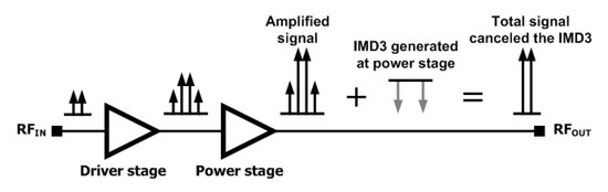
Figure 1.
Principle of third-order intermodulation distortion (IMD3) cancellation in the antiphase technique.
In this work, we investigate the possibility of CMOS PAs with a p-channel metal oxide semiconductor (PMOS) driver stage to suppress the nonlinearities such as IM, AM-AM, and AM-PM distortions. Although, in general, most linear CMOS PAs use n-channel metal oxide semiconductor (NMOS) driver stage, we verify that utilizing the PMOS driver stage could also be one of the candidates of the linearization techniques of CMOS PAs. In general, the PMOS has only been used for a component of the pre-distorter. In this work, we investigate the design methodology to utilize the PMOS itself as the driver stage of the linear CMOS PA without additionally required pre-distorter.
2. Antiphase Technique
We analyze IMD3 and gm3 characteristics of the driver stage according to the bias voltage. To analyze the linearity of the CMOS PA, we use gm,LS and gm3,LS, which are respectively defined as large signals gm and gm3 [16]. The terms gm,LS and gm3,LS are represented by the integration of gm and gm3 inside the input voltage perturbation region as follows:
In the above equations, VP-P and VN,CS,DRV are the peak-to-peak voltage of the input voltage and the common-source gate bias of the driver stage, respectively. Given that the PA is operated at a high power level, a large-signal analysis using the gm,LS and gm3,LS of transistors is necessary for the precise cancellation of the IMD3 [16,17]. Meanings of various symbols used are summarized in the nomenclature section.
2.1. IMD3 in the Middle-Power Region
Figure 2 shows conceptual diagrams of IMD3 of a CMOS PA. To expand the linear region of the PA, the IMD3 cancellation between the driver and power stages is optimized in the high-power region. As shown in Figure 3a,b, to obtain a positive sign of gm3,LS of the driver stage, while the power stage has a negative sign of gm3,LS, the common-source transistor of the driver stage should be biased at the subthreshold region. If the gm3,LS of the driver stage in the subthreshold region is optimized for the gm3,LS of the power stage, the linear region can be successfully expanded.
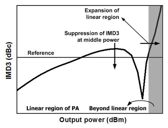
Figure 2.
Conceptual diagrams of IMD3 of power amplifier (PA).
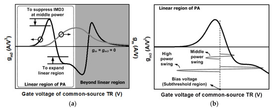
Figure 3.
Conceptual diagram of gm3 of driver stage: (a) gm3, (b) zoomed-in gm3.
However, although the linear region is expanded through the cancellation of the IMD3 between the driver and power stages in the high-power region, the IMD could deteriorate in the middle-power region, as shown in Figure 2 [16,17]. To analyze the IMD3 in the middle-power region, we use the desired voltage, vSig,DRV and the third-order distortion voltage, v3rd,DRV, which are generated in the output of the driver stage as follows [17]:
In the above equation, ZL,DRV, gm,LS,DRV, gm3,LS,DRV, and A are the load impedance, gm,LS, gm3,LS, and amplitude of the two-tone input signal of the driver stage, respectively. In the middle-power region, because A is sufficiently small, the second term of the right-hand side of (3) may be negligible, and we can rewrite (3) as follows:
From (4) and (5), we can calculate the overall third-order distortion voltage of the PA, v3rd,PA in the middle-power region as follows:
In (6), ZL,PW, gm,LS,PW, and gm3,LS,PW are the load impedance, gm,LS, and gm3,LS of the power stage, respectively. In (6), gm3,LS,DRV and gm3,LS,PW should have opposite signs to suppress the IMD3 of the PA for the high-power region.
Although the linearity in the high-power region could be improved by biasing the driver stage in the subthreshold region, the IMD3 in the middle-power region could be deteriorated. Because the driver stage is biased in the subthreshold region, the driver stage operates as class-C. Accordingly, the gm,LS,DRV of (6) is relatively low in the middle-power region compared to the case of the high-power region. Moreover, as depicted in Figure 3b, if the voltage swing of the driver stage is in the middle-power region, the gm3,LS,DRV has a maximum positive value. As a result, if the IMD3 cancellation between the driver and power stages is optimized in the high-power region, the v3rd,PA of (6) is mainly regulated by gm3,LS of the driver stage in the middle-power region. In other words, the deterioration of IMD3s in the middle-power region is caused by the relatively huge IMD3s generated in the driver stage compared with the IMD3 generated in the power stage.
Accordingly, although the positive sign of the gm3 of the driver stage with a subthreshold bias voltage suppresses the IMD3 in the high-power region, the magnitude of gm3 with the positive sign should be reduced to avoid the deterioration of IMD3 in the middle-power region, as shown in Figure 3a.
2.2. Expansion of Linear Region
The positive gm3,LS of the driver stage with subthreshold bias cancels out the negative gm3,LS of the power stage to expand the linear region of the CMOS PA [16]. However, if the magnitude of the positive-sign gm3 of the driver stage in the subthreshold region is reduced to suppress the IMD3 of the middle-power region of the PA, the positive gm3,LS of the driver stage may be insufficient to cancel out the negative gm3,LS of the power stage in the high-power region. Accordingly, an additional strategy to expand the linear region is required.
If we consider gm3,LS instead of gm3 for Figure 3a, the conceptual diagram of gm3,LS can then be shown as Figure 4. For the cancellation of gm3,LSs between the driver and power stages as well as the resulting suppression of the IMD3 in the high-power region, the positive-sign region of gm3,LS of the driver stage should be expanded. One of the solutions to expand the positive region of gm3,LS shown in Figure 4 is to reduce the magnitude of the negative part of gm3 shown in Figure 3a. Hence, the linear region of the PA is expanded, as shown in Figure 2.
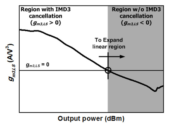
Figure 4.
Conceptual diagram of gm3,LS of driver stage.
In this work, we propose a technique to reduce the magnitude of the positive and negative parts of gm3 of the driver stage to suppress the IMD3 in the middle-power region, as well as to expand the linear region of the PA using bias voltages of the driver stage.
2.3. AM-AM Distortion
In this work, to moderate the breakdown problem of a CMOS PA, we consider the driver stage as a cascode structure. As mentioned in previous sections, because the common-source transistor of the driver stage is operated in the class-C region to complete the antiphase technique, there is a nonlinearity of the gain of the driver stage. In the ideal case, the nonlinearities of the gains of the driver and power stages should be compensated with each other in order to minimize the AM-AM distortion. However, in a real case, the AM-AM distortion of the entire PA may be degraded because of the excessive nonlinearity of the gain of the driver stage.
To analyze and suppress the excessive nonlinearity of the driver stage, we investigate the gate bias of the common-gate transistor of the driver stage. The gate bias of the common-gate transistor could be regulated to improve the linearity of the gain of the driver stage using a common-source transistor biased in the subthreshold region. In this work, we regard the driver stage with a cascode structure as a cascade-connected common-source stage and a common-gate stage [21,22]. The output voltage of the driver stage can then be expressed as follows:
In the above equation, α1 and α3 are the coefficient of the common-source stage. Similarly, β1 and β3 are the coefficients of the common-gate stage. Because the common-source stage is operating as class-C, α1 and α3 have positive values. In addition, if the common-gate stage is operating as class-A or class-AB, β1 and β3 have positive and negative values, respectively.
The conceptual diagram of the gains of the common-source, common-gate, and overall driver stages are shown in Figure 5. Given that the bias of the common-source stage is optimized in the subthreshold region, the values of α1 and α3 have already been fixed. Accordingly, from Figure 5, to improve the linearity of the driver stage, the values of β1 and β3 should be optimized.
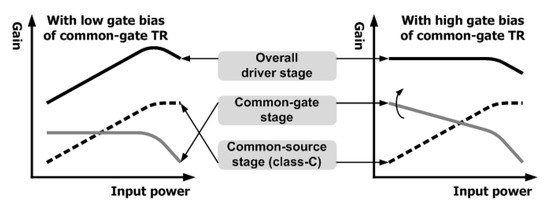
Figure 5.
Conceptual gain of driver stage composed of the cascode structure.
Consequently, from (7) and Figure 5, the gate bias of the common-gate stage of the driver stage should be varied to avoid the excessive nonlinearity of the gain of the driver stage, and hence to suppress the AM-AM distortion of the entire PA.
3. Antiphase Technique Using PMOS Driver Stage
3.1. IMD3 in the Middle-Power Region
As described in Section 2, to suppress IMD3 in the middle-power region, the magnitude of the positive-sign gm3 of the driver stage should be reduced. In this work, we propose a CMOS PA using a driver stage composed of a PMOS to reduce the magnitude of the positive-sign gm3 of the driver stage. To analyze the proposed driver stage using a PMOS, related to the IMD3, we investigate the simplified schematic of a CMOS PA using NMOS and PMOS driver stages, as shown in Figure 6a,b. In this study, to obtain the subthreshold bias voltage of the driver stage for the gm3 cancellation, VN,CS,DRV and VP,CS,DRV are respectively set to 0.47 V and 2.79 V. For the simulation, 3.3 V is used as the value of VDD of the amplifier. Considering the difference in the mobility of electrons and holes, we designed the simulation such that the total gate width, W of the transistor of the PMOS driver stage is two times larger than that of the NMOS driver stage.
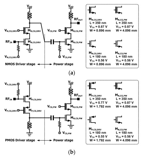
Figure 6.
Simplified schematic of PA (VDD = 3.3 V): (a) n-channel metal oxide semiconductor (NMOS) driver stage, (b) p-channel metal oxide semiconductor (PMOS) driver stage.
Figure 7a,b show the dc-simulated gm and gm3 of the NMOS and PMOS driver stages, respectively. If we consider the subthreshold region, where the gm3 has a positive value, gm, gm2, and gm3 can then be calculated as follows:
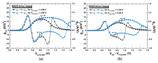
Figure 7.
Simulated gm and gm3 of the driver stage (VDD = 3.3 V): (a) typical NMOS driver stage, (b) proposed PMOS driver stage.
In the above equation, IDS,SUB is the drain current of the driver stage in the subthreshold region. From (8), the positive values of gm3 at the subthreshold region are proportional to the mobility of carrier of MOS. Accordingly, as shown in Figure 7a,b, the magnitude of the positive sign gm3 of the PMOS driver stage is lower than that of the NMOS driver stage. Accordingly, if the PMOS is used as the transistor of the driver stage, we could easily reduce the magnitude of the positive-sign gm3 in the subthreshold region. Consequently, we could expect that the IMD3 in the middle-power region could be successfully suppressed in the case of the PMOS driver stage.
To estimate the IMD3s in the middle-power region of the PA, we simulate the magnitude of IMD3s of the PA with various bias voltages of common-source transistors of the driver stage. Figure 8a shows the IMD3 and gain of a PA with an NMOS driver stage that has various VN,CS,DRV, and a fixed VN,CG,DRV of 2.00 V. Figure 8a shows the optimum IMD3 and gain characteristics with VN,CS,DRV of 0.47 V. Similarly, Figure 8b shows that the optimum value of VP,CS,DRV is 2.79 V with a fixed VP,CG,DRV of 0.35 V. As shown in Figure 8a,b, the magnitude of IMD3s with a PMOS driver stage is relatively lower than that with an NMOS driver stage in the middle-power region.
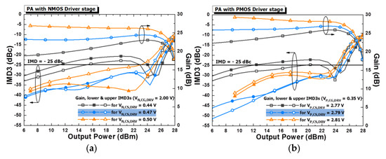
Figure 8.
Simulated IMD3 and gain with various common-source bias voltages (VDD = 3.3 V, VN,CG,DRV = 2.00 V, and VP,CG,DRV = 0.35 V): (a) typical NMOS driver stage, (b) proposed PMOS driver stage.
3.2. Expansion of Linear Region
As the magnitude of the positive gm3 is reduced in the proposed PMOS driver stage, the positive region of gm3,LS is also reduced, and hence the linear region as well, as can be predicted in Figure 4. To expand the linear region of Figure 4 using a positive gm3 with a given magnitude, the magnitude of the negative gm3 should be reduced. In this work, we choose to optimize the value of VP,CG,DRV to reduce the magnitude of the negative gm3. If VP,CG,DRV decreases with a fixed VP,CS,DRV (=2.79 V), the drain voltage of MP,CS,DRV decreases. The saturation region of MP,CS,DRV is therefore expanded according to the decreased VP,CG,DRV. The reason for the expansion of the saturation region of MP,CS,DRV with the decreased VP,CG,DRV will be described in Section 4. If the saturation region is expanded and we consider the linear region of the PA, the variation of gm2, and hence the magnitude of negative gm3, is reduced in the saturation region. As shown in Figure 7b, with a VP,CG,DRV value of 0.35 V, the magnitude of negative gm3 is reduced when compared to what is obtained with a VP,CG,DRV value of 1.30 V. This phenomenon can be also verified in Figure 9. Because the magnitude of negative gm3 with VP,CG,DRV of 0.35 V is reduced, the positive regions of gm3,LS is expanded. Consequently, with a reduced VP,CG,DRV, the region of IMD3 cancellation between the driver and power stages, and hence the linear region of the entire PA, is expanded. In this work, from the perspective of the expansion of the linear region, the optimum value of VP,CG,DRV is 0.35 V.
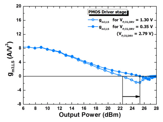
Figure 9.
Simulated gm3,LS according to the output power of the PMOS driver stage (VDD = 3.3 V and VP,CS,DRV = 2.79 V).
3.3. AM-AM Distortion
As mentioned in previous sections, the AM-AM distortion of the entire PA may be degraded because of the excessive nonlinearity of the gain of the driver stage. Figure 10 shows the IMD3 and gain of a PA with a PMOS driver stage that has various values of VP,CG,DRV, and with a fixed VP,CS,DRV of 2.79 V. As the VP,CG,DRV decreases, the gain of the common-gate stage increases. Accordingly, the gain of the driver stage in the low- and middle-power region can increase, and therefore the AM-AM distortion can be suppressed.
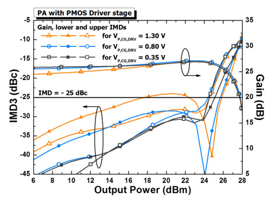
Figure 10.
Simulated IMD3 and gain of proposed PMOS stage with various common-gate bias voltage (VDD = 3.3 V and VP,CS,DRV = 2.79 V).
In this study, we choose 0.35 V as the optimum value of VP,CG,DRV for a reasonable AM-AM distortion level. At the same time, as described in the previous sections, the value of 0.35 V for VP,CG,DRV is also the optimum value for the suppression of IMD3. Consequently, the values of 0.35 V and 2.79 V for VP,CG,DRV and VP,CS,DRV are optimum points for the simultaneous suppression of IMD3 and AM-AM distortion.
4. Technique of Suppression of AM-PM Distortion
In this work, we also try to suppress the AM-PM distortion using the driver stage. If the power stage is composed of a common-source or cascode structure, the parasitic capacitance between the gate and source of the common-source transistor, CGS,CS,P, mainly affects the phase of the power stage. In general, if the input voltage swing is considered and the power stage is composed of n-type MOS (NMOS), the average CGS,CS,P according to the input power gradually decreases as the input power increases. Accordingly, to compensate for the variation of CGS,CS,P and hence the variation in the phase of the output of the PA, the average parasitic capacitance between the gate and source of the common-source transistor of the driver stage, CGS,CS,D, should gradually increase as the input power increases.
Figure 11a shows the proposed PA with a PMOS driver stage with 1.3 V as the gate bias of MP,CG,DRV. Because the driver stage of the proposed PA is composed of a PMOS, if the input power of the driver stage increases as shown in Figure 11a, the average CGS,CS,D increases. However, if the input voltage increases further and exceeds the boundary between the triode and saturation regions of MP,CS,DRV, the average CGS,CS,D slightly decreases. Consequently, at the high-power region, the compensation mechanism is broken if the input voltage of the driver stage exceeds the boundary between the triode and saturation regions. To expand the capacitance compensation region, the region of saturation of MP,CS,DRV should also be expanded. In this work, we regulate the value of VP,CG,DRV to expand the saturation region of MP,CS,DRV. As depicted in Figure 11b, if VP,CG,DRV decreases, the drain voltage of MP,CS,DRV, VD,CS, also decreases and hence expands the saturation region of MP,CS,DRV. Accordingly, the region where the slope of the graph of the average CGS,CS,D according to the RFIN is positive can then be expanded, as shown in Figure 11b. Consequently, when regulating VP,CG,DRV, the region where the mechanism of compensation between the average CGS,CS,D and CGS,CS,P occurs is expanded toward the high-power region.
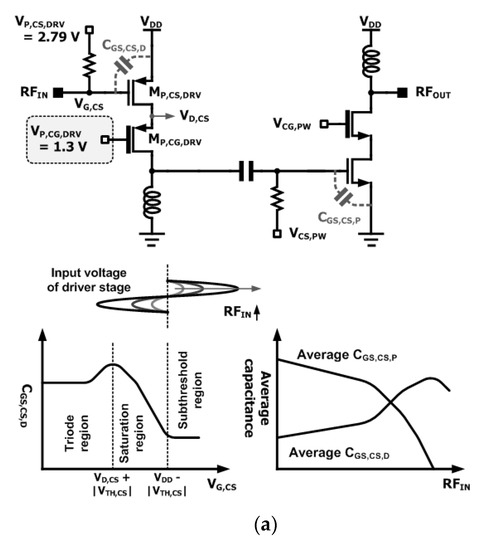
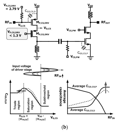
Figure 11.
Conceptual parasitic capacitances of power and driver stages (VDD = 3.3 V): (a) 2.79 V of VP,CS,DRV, (b) decreased value of VP,CS,DRV.
Figure 12 shows the simulated CGS,CS,D of the PMOS driver stage according to the input power of the driver stage. As can be seen in Figure 12, using VP,CG,DRV, compared with the conceptual CGS,CS,D shown in Figure 11b, the saturation region of MP,CS,DRV is successfully expanded with a VP,CG,DRV value of 0.35 V. To prove the improvements in the AM-PM distortion of the proposed PA while optimizing the value of VP,CG,DRV, the simulated output phases of the PA with respect to various VP,CG,DRV are compared in Figure 13. The value of VP,CS,DRV is fixed at 2.79 V for this simulation. With a VP,CG,DRV, of 0.35 V, the variation in the output phase of the PA in the region from −20 dBm to 0 dBm is suppressed below 0.6°. The region of the input power from −20 dBm to 0 dBm is approximately the linear region of the entire PA.
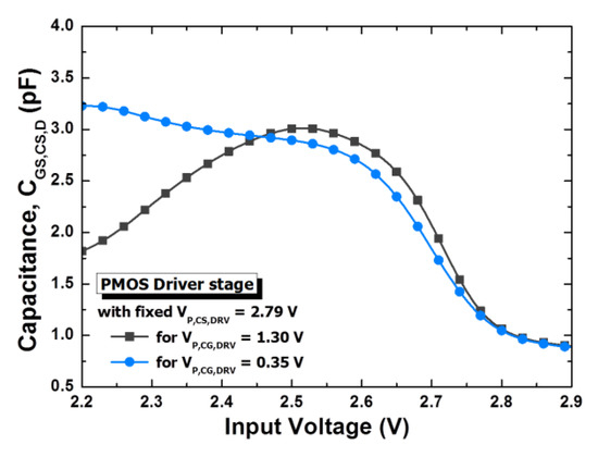
Figure 12.
Simulated CGS,CS,D according to the input voltage, VG,CS of the PMOS driver stage with 1.30 V and 0.35 V of VP,CG,DRV (VDD = 3.3 V).
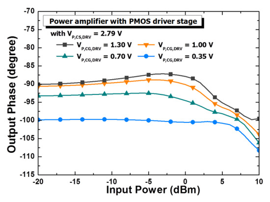
Figure 13.
Simulated output phase of the proposed PA with PMOS driver stage (VDD = 3.3 V).
Fortunately, the value of the optimum value of VP,CG,DRV for the suppressed AM-PM distortion coincides with the optimum value of the VP,CG,DRV for the suppressed IMD3 and AM-AM distortion, as mentioned in the previous section.
5. Implementation and Measured Results
5.1. Implementation
Figure 14 shows the schematic of the proposed CMOS PA In this study, we use differential and cascode structures to moderate the gain reduction induced by the bond-wires and the low breakdown problems, respectively. To obtain stability of the designed PA, the RC feedback technique is applied to the power stage of the amplifier. Further, a second harmonic termination technique using an metal-insulator-metal (MIM) capacitor and bond-wire is applied to the gate nodes of MP,CG,DRV and MN,CG,PW to suppress the asymmetries between upper and lower IMD3s.
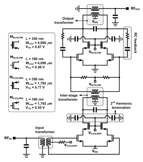
Figure 14.
Schematic of proposed complementary metal-oxide semiconductor (CMOS) PA (VDD = 3.3 V).
The detailed transistor sizes are included in Figure 14. The input transformer had a 1:2 turn ratio with primary and secondary windings having 10 μm metal width of primary and secondary windings. The inter-stage transformer had a 2:1 turn ratio with primary and secondary windings had a 15 μm metal width of primary and secondary windings. The output transformer had a 1:2 turn ratio with primary and secondary windings of 40 μm and 25 μm metal widths, respectively.
5.2. Measured Results
Figure 15 shows a chip photograph of the designed CMOS PA with a size of 0.9 mm × 2.0 mm, including all of the test pads. The PA was designed using a 180 nm RFCMOS process that provides one poly and six metal layers. For the measurement, the fabricated PA was mounted on the RF4 printed circuit board, and bond-wires for the RF input, RF output, various bias voltages, supply voltage, and ground are used. For the measurement, 3.3 V were used as VDD of the designed PA.
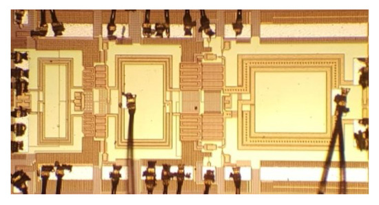
Figure 15.
Photograph of the designed CMOS PA.
Figure 16 shows the measured gain and power-added efficiency (PAE) with a two-tone signal. As can be seen in Figure 16, the value of 0.40 V for the VP,CG,DRV with VP,CS,DRV of 2.75 V is the optimum value associated with the AM-AM distortion. If the value of VP,CG,DRV decreases below 0.40 V, the AM-AM distortion deteriorates.
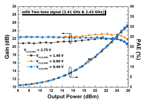
Figure 16.
Measured results: power-added efficiency (PAE) and gain according to output power with a two-tone signal.
Figure 17a shows the IMD3 for various values of VP,CS,DRV with two-tone signals. In this work, because the 802.11 n modulated signal has a center frequency of 2.42 GHz with a 20-MHz bandwidth, we use the two-tone signals of 2.41 GHz and 2.43 GHz. As can be seen in Figure 17a, with when VP,CS,DRV is 2.75 V, the measured output power is measured to be 23.1 dBm when the IMD3 level is −25 dBc. When VP,CS,DRV is 2.75 V, the IMD3 in the middle-power region is suppressed by approximately 2 dB when compared with other VP,CS,DRV cases. In addition, the linear power is expanded by approximately 1 dB. Figure 17b shows the IMD3 for various values of VP,CG,DRV with two-tone signals. In this case, the value of VP,CS,DRV is fixed at 2.75 V. A similar analysis could be applied to both Figure 17a,b. Consequently, from the measured results of Figure 17, which are related to the linearity of the designed PA, the optimum values of VP,CS,DRV and VP,CG,DRV are 2.75 V and 0.40 V, respectively.
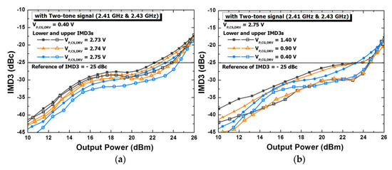
Figure 17.
Measured results: IMD3s with two-tone signal for the various gate bias values: (a) VP,CS,DRV, (b) VP,CG,DRV.
Figure 18a,b show the measured EVMs with fixed VP,CG,DRV and VP,CS,DRV, respectively. In this measurement, we use the modulated signal of 802.11 n with a 20-MHz bandwidth and 64-quadrature amplitude modulation (QAM) (MCS7) 65-Mb/s. As predicted from the simulated results of Figure 12 and Figure 13, there exist optimum values for VP,CG,DRV and VP,CS,DRV. From the measured results, the optimum values of VP,CG,DRV and VP,CS,DRV are 2.75 V and 0.40 V, respectively. The measured maximum output power is 22.1 dBm, which satisfies an EVM of 3.98%.
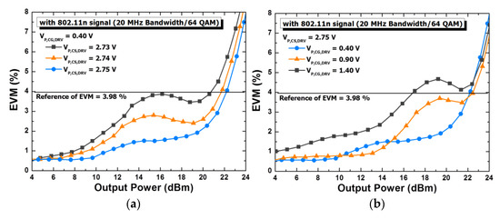
Figure 18.
Measured results: error vector magnitude (EVM)3s with 802.11 n modulated signal for the various gate bias values (a) VP,CS,DRV, (b) VP,CG,DRV.
Figure 19 shows the measured spectrum mask for an average output power of 21.5 dBm with a 2.4 GHz 802.11 n modulated signal of 20 MHz bandwidth and 64 QAM. As shown in Figure 10 and Figure 13, the output phase, which affects the EVM property, is flat up to an input power of 5 dBm, while the sweet spot, which affects the spectrum mask, occurs at an input power of −2 dBm. Similarly, the measured output power that satisfies 3.98% of EVM is higher than the maximum linear output power, which satisfies the spectrum mask of the 802.11 n standard. Consequently, although the measured output power with an EVM of 3.98% is 22.1 dBm, the measured maximum linear output power, PMAX, was 21.5 dBm.
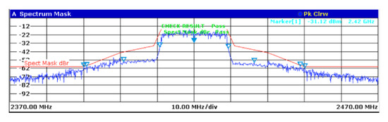
Figure 19.
Measured results: spectrum mask at the output power of 21.5 dBm with 802.11 n signals with 20 MHz/64 quadrature amplitude modulation (QAM) at 2.42 GHz.
Figure 20 shows the measured PAE and gain of the amplifier with an 802.11 n modulated signal. The measured optimum values for VP,CS,DRV and VP,CG,DRV are 2.75 V and 0.40 V, respectively. The measured PAE was 23.4% for a PMAX value of 21.5 dBm, where EVM and the spectrum mask for the 802.11 n standard are satisfied at the same time. The measured value of EVM was 3.14% for a PMAX of 21.5 dBm. The measured gain was approximately 24 dB. In Table 1, we summarize the performances of recent CMOS power amplifiers for WLAN applications.
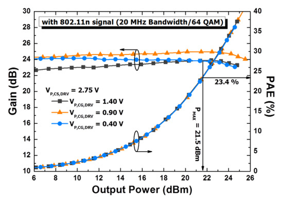
Figure 20.
Measured results: PAE and gain according to output power with 802.11 n modulated signal.

Table 1.
Summary and Performance comparison of recent CMOS power amplifier for WLAN.
6. Conclusions
In this study, we propose a CMOS PA using a PMOS driver stage to enhance linearity. To suppress the IMD3 of the entire PA, we propose a biasing methodology of the PMOS driver stage to cancel out the IMD3s between the driver and power stages. Using optimum bias voltages of common-source and cascode transistors of the PMOS driver stage, we find the IMD3 cancellation and the expansion of the linear region of the entire PA. In addition, by analyzing the characteristic of the AM-AM and AM-PM distortions of the PMOS driver stage, we also propose a biasing methodology to suppress the EVM of the entire PA. Consequently, we verified that the proposed PMOS driver stage acts as the pre-distorter, as well as the driver stage of the power stage. We designed the proposed CMOS PA using a 180-nm RFCMOS process for WLAN 802.11 n applications. We obtained a maximum linear output power of 21.5 dBm with a PAE of 23.4%. From the measured results, we successfully verified the feasibility of using the PMOS driver stage for the CMOS PA to enhance linearity.
Author Contributions
Conceptualization, formal analysis, and investigation, J.K., C.L. and C.P.; methodology, validation, and data curation, J.K.; writing—original draft preparation, writing—review and editing, and visualization, J.K. and J.Y.; supervision, project administration, and funding acquisition, C.P. All authors have read and agreed to the published version of the manuscript.
Funding
This research received no external funding.
Acknowledgments
This work was supported by the Development of Civil Military Technology program (No. 17-CM-MC-08) from the Institute of Civil Military Technology Cooperation (ICMTC).
Conflicts of Interest
The authors declare no conflict of interest.
Nomenclature
| gm,LS | |
| Large signal gm | |
| gm3,LS | Large signal gm3 |
| gm,LS,DRV | gm,LS of two-tone input signal of driver stage |
| gm3,LS,DRV | gm3,LS of two-tone input signal of driver stage |
| gm,LS,PW | gm,LS of power stage |
| gm3,LS,PW | gm3,LS of power stage |
| A | Amplitude of two-tone input signal of driver stage |
| ZL,DRV | Load impedance of two-tone input signal of driver stage |
| ZL,PW | Load impedance of power stage |
| vSig,DRV | Desired signal voltage |
| v3rd,DRV | Third-order distortion voltage |
| v3rd,PA | Overall third-order distortion voltage of power amplifier |
| IDS,SUB | Drain current of driver stage in the subthreshold region |
| VP-P | Peak-to-Peak voltage of the input voltage of driver stage |
| VDD | |
| Supply voltage | |
| VN,CS,DRV | Common-source gate bias of NMOS driver stage |
| VP,CS,DRV | Common-source gate bias of PMOS driver stage |
| VN,CG,DRV | Common-gate gate bias of NMOS driver stage |
| VP,CG,DRV | Common-gate gate bias of PMOS driver stage |
| MN,CS,DRV | Common-source transistor of NMOS driver stage |
| MN,CG,DRV | Common-gate transistor of NMOS driver stage |
| MP,CS,DRV | Common-source transistor of PMOS driver stage |
| MP,CG,DRV | Common-gate transistor of PMOS driver stage |
| MN,CS,PW | Common-source transistor of NMOS power stage |
| MN,CG,PW | Common-gate transistor of NMOS power stage |
| CGS,CS,P | CGS of common-source transistor of power stage |
| CGS,CS,D | CGS of common-source transistor of driver stage |
References
- Kang, D.; Park, B.; Kim, D.; Kim, J.; Cho, Y.; Kim, B. Envelope-tracking CMOS power amplifier module for LTE applications. IEEE Trans. Microw. Theory Tech. 2013, 61, 3763–3773. [Google Scholar] [CrossRef]
- Park, S.; Woo, J.-L.; Kwon, Y. Broadband CMOS stacked RF power amplifier using reconfigurable interstage network for wideband envelope tracking. IEEE Trans. Microw. Theory Tech. 2015, 63, 1174–1185. [Google Scholar] [CrossRef]
- Kim, J.; Yoon, Y.; Kim, H.; An, K.H.; Kim, W.; Kim, H.-W.; Lee, C.-H.; Kornegay, K.T. A linear multi-mode CMOS power amplifier with discrete resizing and concurrent power combining structure. IEEE J. Solid State Circuits 2011, 46, 1034–1048. [Google Scholar]
- Hassan, M.; Larson, L.E.; Leung, V.W.; Kimball, D.F.; Asbeck, P.M. A wideband CMOS/GaAs HBT envelope tracking power amplifier for 4G LTE mobile terminal applications. IEEE Trans. Microw. Theory Tech. 2012, 60, 1321–1330. [Google Scholar] [CrossRef]
- Son, M.; Yoo, J.; Kang, I.; Lee, C.; Kim, J.; Park, H.J.; Park, Y.-B.; Park, C. RF CMOS power amplifier using a split inter-stage inductor for IEEE 802.11n applications. Int. J. Microw. Wirel. Technol. 2017, 9, 719–727. [Google Scholar] [CrossRef]
- Sim, Y.; Park, J.; Yoo, J.; Lee, C.; Park, C. A CMOS power amplifier using an active balun as a driver stage to enhance its gain. Microelectron. J. 2017, 63, 160–169. [Google Scholar] [CrossRef]
- Hwang, H.; Lee, C.; Park, J.; Park, C. A current-shared cascade structure with an auxiliary power regulator for switching mode RF power amplifiers. IEEE Trans. Microw. Theory Tech. 2014, 62, 2711–2722. [Google Scholar] [CrossRef]
- Lee, C.; Yoon, S.; Park, C. A differentially coupled series inductor for differential RFICs. Microw. Opt. Technol. Lett. 2015, 57, 2223–2225. [Google Scholar] [CrossRef]
- Golara, S.; Moloudi, S.; Abidi, A.A. Process of AM-PM distortion in large signal single-FET amplifiers. IEEE Trans. Circuits Syst. I Regul. Pap. 2017, 64, 245–260. [Google Scholar] [CrossRef]
- Joo, T.; Koo, B.; Hong, S. A WLAN RF CMOS PA with large signal MGTR method. IEEE Trans. Microw. Theory Tech. 2013, 61, 1272–1279. [Google Scholar] [CrossRef]
- Onizuka, K.; Ishihara, H.; Hosoya, M.; Saigusa, S.; Watanabe, O.; Otaka, S. A 1.9 GHz CMOS power amplifier with embedded linearizer to compensate AM-PM distortion. IEEE J. Solid State Circuits 2012, 47, 1820–1827. [Google Scholar] [CrossRef]
- Koo, B.; Na, Y.; Hong, S. Integrated bias circuits of RF CMOS cascode power amplifier for linearity enhancement. IEEE Trans. Microw. Theory Tech. 2012, 60, 340–351. [Google Scholar] [CrossRef]
- Wang, C.; Vaidyanathan, M.; Larson, L.E. A capacitance compensation technique for improved linearity in CMOS class-AB power amplifiers. IEEE J. Solid State Circuits 2004, 39, 1927–1937. [Google Scholar] [CrossRef]
- Kulkarni, S.; Reynaert, P. A 60-GHz power amplifier with AM-PM distortion cancellation in 40-nm CMOS. IEEE Trans. Microw. Theory Tech. 2016, 64, 2284–2291. [Google Scholar] [CrossRef]
- Vigilante, M.; Reynaert, P. A wideband class-AB power amplifier with 29-57-GHz AM-PM compensation in 0.9-V 28-nm Bulk CMOS. IEEE J. Solid State Circuits 2018, 53, 1288–1301. [Google Scholar] [CrossRef]
- Park, J.; Lee, C.; Park, C. A quad-band CMOS linear power amplifier for EDGE applications using an anti-phase method to enhance its linearity. IEEE Trans. Circuits Syst. I Regul. Pap. 2016, 64, 765–776. [Google Scholar] [CrossRef]
- Park, J.; Lee, C.; Park, C. A CMOS antiphase power amplifier with an MGTR technique for mobile applications. IEEE Trans. Microw. Theory Tech. 2017, 65, 4545–4656. [Google Scholar] [CrossRef]
- Choi, K.; Kim, M.; Kim, H.; Jung, S.; Cho, J.; Yoo, S.; Kim, Y.H.; Yoo, H.; Yang, Y. A highly linear two-stage amplifier integrated circuit using InGaP/GaAs HBT. IEEE J. Solid State Circuits 2010, 45, 2038–2043. [Google Scholar] [CrossRef]
- Kang, J.; Yoon, J.; Min, K.; Yu, D.; Nam, D.; Yang, Y.; Kim, B. A highly linear and efficient differential CMOS power amplifier with harmonic control. IEEE J. Solid State Circuits 2006, 41, 1314–1322. [Google Scholar] [CrossRef]
- Lee, S.; Nam, S. A CMOS outphasing power amplifier with integrated single-ended chireix combiner. IEEE Trans. Circuits Syst. II Express Briefs 2010, 45, 411–415. [Google Scholar]
- Jin, S.; Park, B.; Moon, K.; Kwon, M.; Kim, B. Linearization of CMOS cascade power amplifiers through adaptive bias control. IEEE Trans. Microw. Theory Tech. 2013, 61, 4534–4543. [Google Scholar] [CrossRef]
- Jin, S.; Kwon, M.; Moon, K.; Park, B.; Kim, B. Control of IMD asymmetry of CMOS power amplifier for broadband operation using wideband signal. IEEE Trans. Microw. Theory Tech. 2013, 61, 3753–3762. [Google Scholar] [CrossRef]
- Kaymaksut, E.; Reynaert, P. Transformer based uneven Doherty power amplifier in 90 nm CMOS for WLAN applications. IEEE J. Solid State Circuits 2012, 47, 1659–1671. [Google Scholar] [CrossRef]
- Yin, Y.; Yu, X.; Wang, Z.; Chi, B. An efficiency-enhanced stacked 2.4-GHz CMOS power amplifier with mode switching scheme for WLAN applications. IEEE Trans. Microw. Theory Tech. 2015, 63, 672–682. [Google Scholar] [CrossRef]
- Jeong, G.; Kang, S.; Joo, T.; Hong, S. An integrated dual-mode CMOS power amplifier with linearizing body network. IEEE Trans. Circuits Syst. II Express Briefs 2017, 64, 1037–1041. [Google Scholar] [CrossRef]
© 2020 by the authors. Licensee MDPI, Basel, Switzerland. This article is an open access article distributed under the terms and conditions of the Creative Commons Attribution (CC BY) license (http://creativecommons.org/licenses/by/4.0/).