1. Introduction
The down-conversion mixer is a critical block in the design of systems based on the software-defined radio (SDR) architecture. Due to technology limits of the analog to digital converters (ADC), the RF signals at high frequency cannot be directly sampled. The mixer is, thus, a key component to perform the down-conversion of the antenna signal at intermediate frequencies compatible with commercial ADCs.
In literature, several approaches were introduced to maximize the mixer performance. For example, Wei et al. [
1] use a folded topology to diminish the transistors stacked on top of each other. With a folded structure, the circuit can employ a lower supply voltage, however, it requires an extra current source that has the negative effect of reducing both gain and bandwidth. MacEachern et al. [
2] propose a topology that relies on the charge injection method. Their approach allows to improve both gain and linearity, however, it has the drawback that requires a significantly higher bias current and hence it worsens power consumption. Seo et al. [
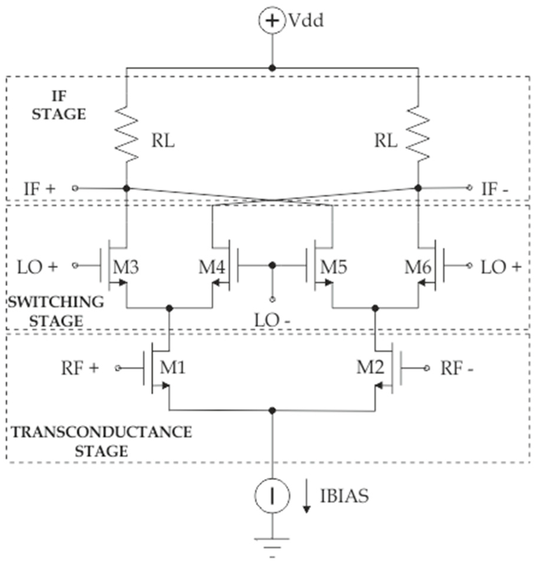
3] exploit a switched biasing technique for the tail current source that results in a substantial reduction of the noise figure. Unfortunately, this benefit comes at the expenses of a significantly larger supply voltage and power dissipation than the traditional Gilbert’s cell. Hence, these approaches utilize very complicated hardware solutions to maximize the performance of the mixer. This work presents the design approach followed to optimize the circuit of a conventional double-balanced Gilbert mixer cell (
Figure 1).
This architecture is very common in homodyne (also known as direct-conversion) receivers because it exhibits a favorable port-to-port isolation factor and negligible even harmonic distortion [
4]. Unfortunately, the presence of three MOS transistor pairs on top of each other calls for a relatively large supply voltage to keep them operating in saturation.
As illustrated in
Figure 1, the RF voltage is fed into the stage consisting of the transistors M1 and M2. The transistors M3–M6, perform RF voltage-to-current conversion and switch the polarity of the RF inputs at the LO frequency rate. In theory, given the symmetry of the circuit, any common-mode RF and LO frequency component at the output should be zero.
This paper aims to extend the Jespers and Murmann g
m/I
D-based approach [
5,
6] to optimize the design of a double-balanced mixer based on the Gilbert cell. A new set of lookup tables were computed to take into account the performance of the mixer in the three MOSFET inversion regions. With these new set of lookup tables, the designer is able to maximize the overall performance of the basic cell without introducing complex circuit solutions. The reported mixer was used in the design of the positioning system reported in [
6,
7,
8,
9].
The rest of the paper is arranged as follow.
Section 2 introduces the methodology we applied to overcome the inaccuracies associated with the traditional square law model of the MOSFET devices.
Section 3 describes the design methodology introduced to maximize the performance of the Gilbert cell.
Section 4 presents the results achieved and compares them with other works presented in the literature. Finally,
Section 5 provides a set of conclusions and closes the paper.
2. Theoretical Background
The traditional approach to design analog circuits is based on modeling the drain current I
D of MOSFET devices in saturation region with the following square law Equation (1)
where μ is the mobility of the carriers in the inversion layer channel, C
ox is the gate oxide capacitance, W/L is the ratio between the width and the channel length of the MOSFET, V
GS is the gate-source voltage and, finally, V
TH is the MOSFET threshold voltage. Given the continuous shrinking of the channel length of the MOSFETs employed in today’s integrated circuits, Equation (1) becomes grossly inaccurate. With the current nanometer channel lengths, several second-order effects are no longer negligible and must be considered [
10].
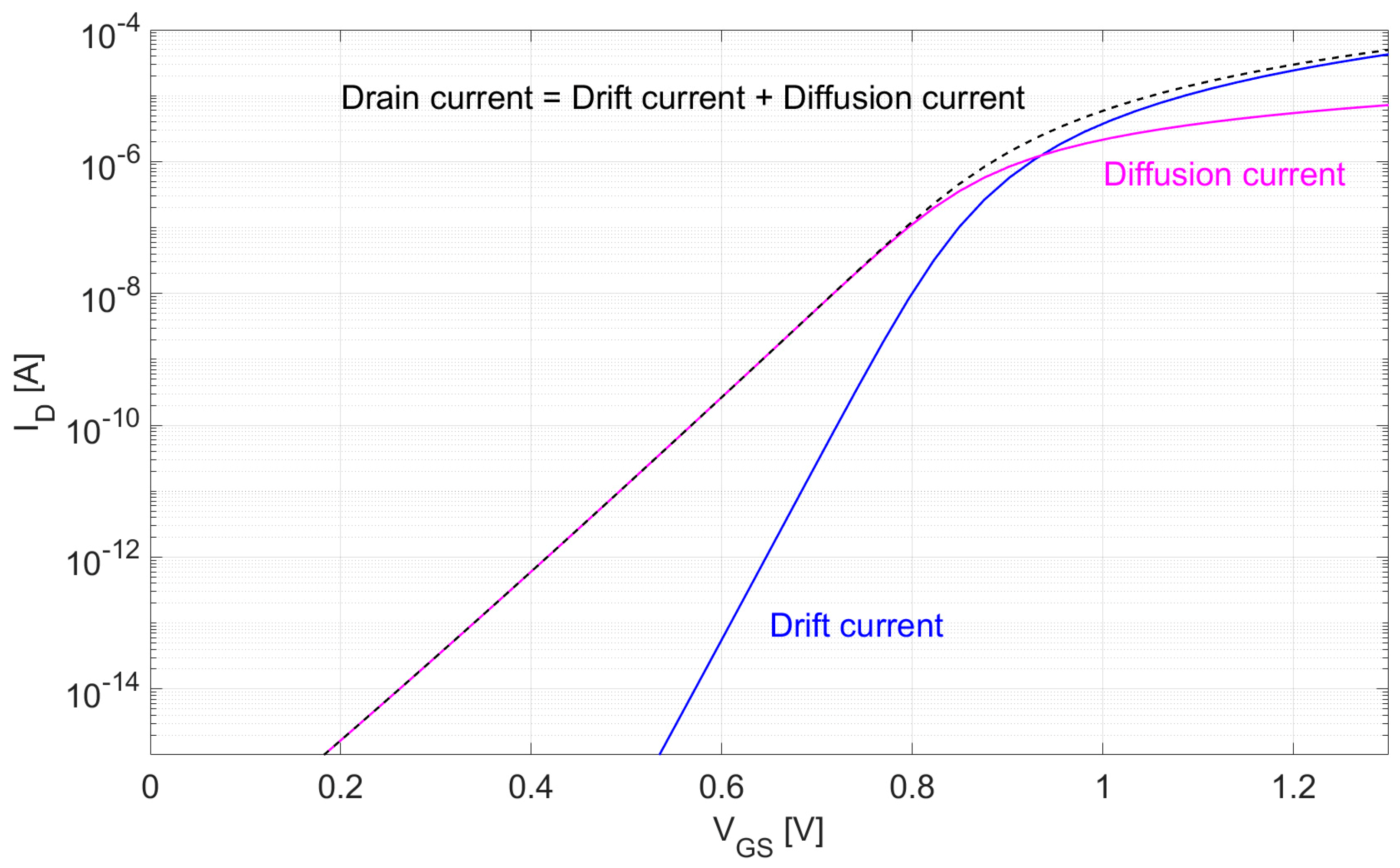
The typical models used for describing the behavior of nanoscale MOSFETs includes several hundred parameters, thus, it is too complicated to come up with a simple analytical abstraction that would be suitable for analog circuit design. When V
GS ≤ V
TH (sub-threshold operation) the drain current does not go to zero as predicted by the square-law equation. The current in and near sub-threshold takes an exponential form. This is because the MOSFET acts as if it was a lateral BJT. In sub-threshold (also known as weak inversion) the current is mainly dominated by its diffusion component (rather than its drift component) and as a result, it has an expression that resembles closely the current equation of a BJT [
11] (
Figure 2):
where k is the Boltzman constant, q is the electronic charge measured in Coulomb, T is the temperature, and m is a coefficient accounting for how the body effect at the drain end of the channel affects the control of the charge in the channel. The coefficient m (also known as the subthreshold factor) is process dependent and it typically varies between 1.3 and 1.7. [
12].
In weak inversion, the current available to drive any capacitive load is quite small so the MOSFET consumes very little power, but it can be quite slow. In addition, the definition of V
TH is problematic. On the contrary, if the transistor operates in strong inversion it consumes more power but exhibits the best performance in terms of speed. The operation between strong and weak inversion is called moderate inversion and due to the growing demand for low supply voltage applications, it has become more and more attractive. In moderate inversion, the MOSFET achieves the best tradeoff between speed and DC-power consumption. Unfortunately, no simple analytical equation exists for the drain current of a MOSFET in moderate inversion. The EKV model [
13], the BSIM model [
14], the ACM model [
15], and the PSP model [
16] on which most simulation tools rely are too complicated for hand analysis.
Using a table-based procedure like the g
m/I
D methodology is more effective. It allows the ability to achieve accurate results with a very limited number of design iterations. This method consists of generating a set of lookup tables starting from the DC-analysis of the transistor. Each table computes a different width-independent figure of merit (FOM), closely linked to the design specifications (e.g., transit frequency, intrinsic gain, transconductance efficiency, current density, and relative capacitances). The design process consists in choosing the inversion level of the MOSFETs so that the figures of merit extracted, and the W/L ratios associated with each transistor are able to meet the required design specifications [
6,
10]. The g
m/I
D ratio, also known as the transconductance efficiency or gain-power efficiency, is a proxy for the inversion level the transistor. Using, for simplicity, the square-law model, for a MOSFET operating in saturation region, the transconductance g
m is defined as:
Hence the g
m over I
D ratio depends only on the overdrive voltage V
OV = V
GS – V
TH.
In other words, setting the gm/ID ratio is equivalent to setting the operating region of the MOSFET. For values of gm/ID between 5 S/A and 8 S/A the MOSFET is in strong inversion. For gm/ID in the range between 20 S/A and 25 S/A the MOSFET is in weak inversion. The choice of the inversion level is essentially determined by the trade-off between speed (transit frequency, fT = gm/CGG), intrinsic gain (gm/gDS), and gain-power efficiency (gm/ID) and it depends on the target application.
The key feature that makes the table-based design approach suggested so effective is that all FOMs are width independent. If for sake of simplicity we resort again to the square-law, we note that:
In strong inversion (low gm/ID ratio) the transistor exhibits higher speed than in weak inversion, but the intrinsic gain is lower, and the power dissipation is higher (to obtain a given value of gm the drain current required is higher than in weak inversion). In weak inversion, that is, for a large gm/ID ratio, the intrinsic gain increases, while the fT decreases. This is due to the corresponding increase of the width of the transistor its total intrinsic capacitances. Finally, the drain current decreases for increasing values of gm/ID, which means that the DC power consumption drops. The region in the middle between strong and weak inversion is called moderate inversion and usually gives a good compromise in terms of speed, gain, and power consumption.
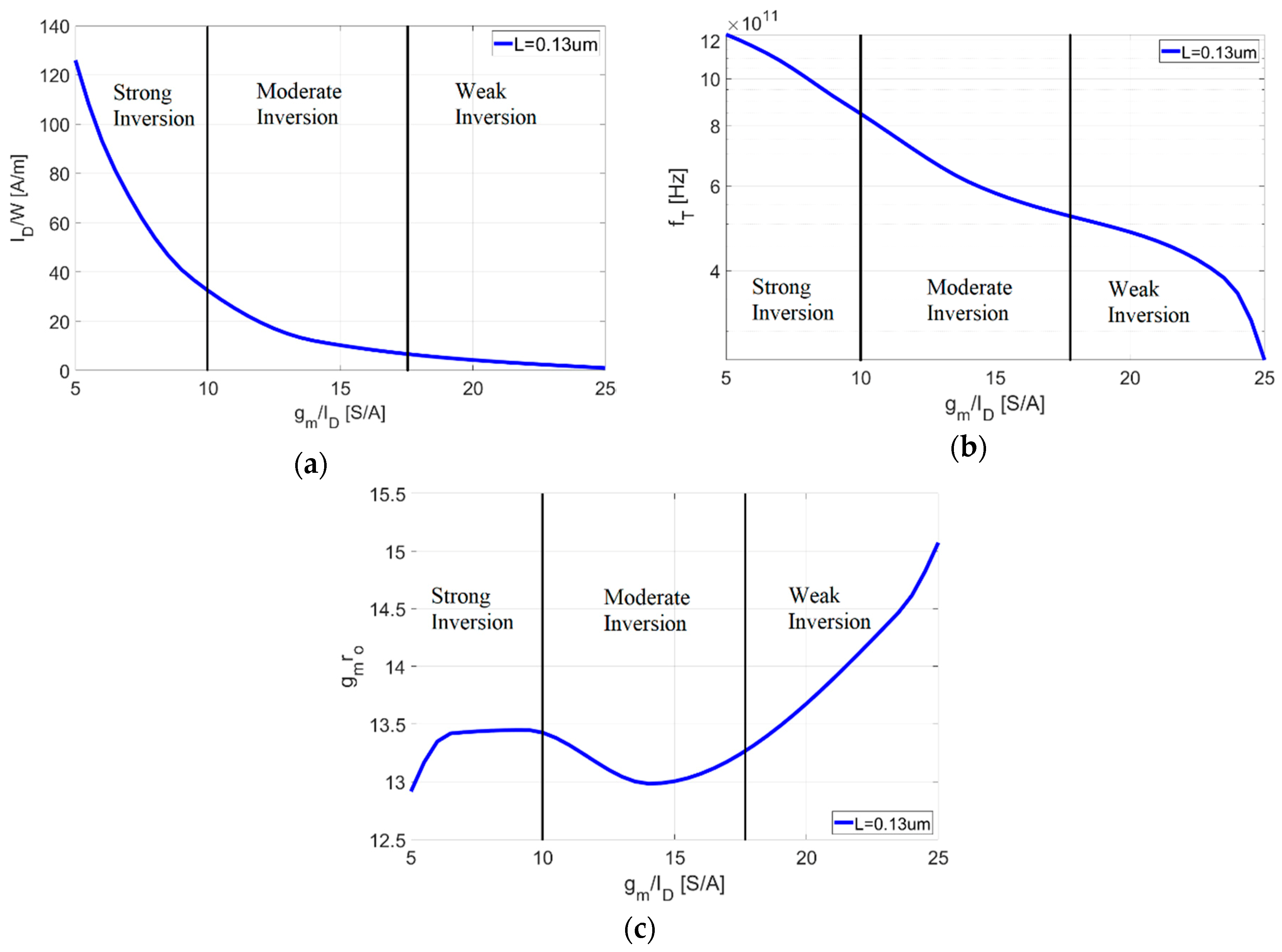
Figure 3 shows the graphs for transit frequency, intrinsic gain and current density versus g
m/I
D for the NMOS transistor from the IHP (Innovate for High-Performance Microelectronics) process [
17,
18,
19,
20,
21,
22] used for implementing the mixer. The curves are sketched for the minimum channel lengths (L = and for a drain-source voltage, V
DS, equal to half the DC-power supply, V
DD. The g
m/I
D design method is both scalable and easily adaptable to the design of different target systems. These charts represent the starting point for implementing the design. The design flow proposed provides the designer with the flexibility to start by choosing any of the tabulated figures of merit as his primary objective and then proceed by systematically extracting all other features depending on the specific performances to be optimized.
3. Design Optimization
For Gilbert’s cell (
Figure 1), given the desired value of the load resistance, R
L, the mixer gain (A
v) is determined by the transconductance value (g
m) of the transistors M1 and M2:
The traditional design approach starts from Equation (6) by first computing the g
m necessary to obtain the desired gain and then choosing the width W and channel length L of the MOSFETs using the square law Equation (7):
where C
ox is the oxide capacitance of the MOSFET and the µ the mobility of the carriers. The bias current supplied by the tail current source (I
BIAS) is split equally among the transistors in the transconductance stage (TS). Similarly, the current flowing through M1 and M2 is evenly split between the transistors in the switching stage (SS):
Unfortunately, in today’s nanometer integrated circuits, the behavior of the MOS transistors does not follow the square-law model. For this reason, in the approach we advocate, the W/L ratio of the transistors is chosen using g
m/I
D-based lookup tables. The algorithm used to optimize the sizing of the transistors considers the devices in the switching stage and the transconductance stage separately. The algorithm allows exploring a larger solution space to find the optimal bias point that meets design specifications, by separately sweeping the g
m/I
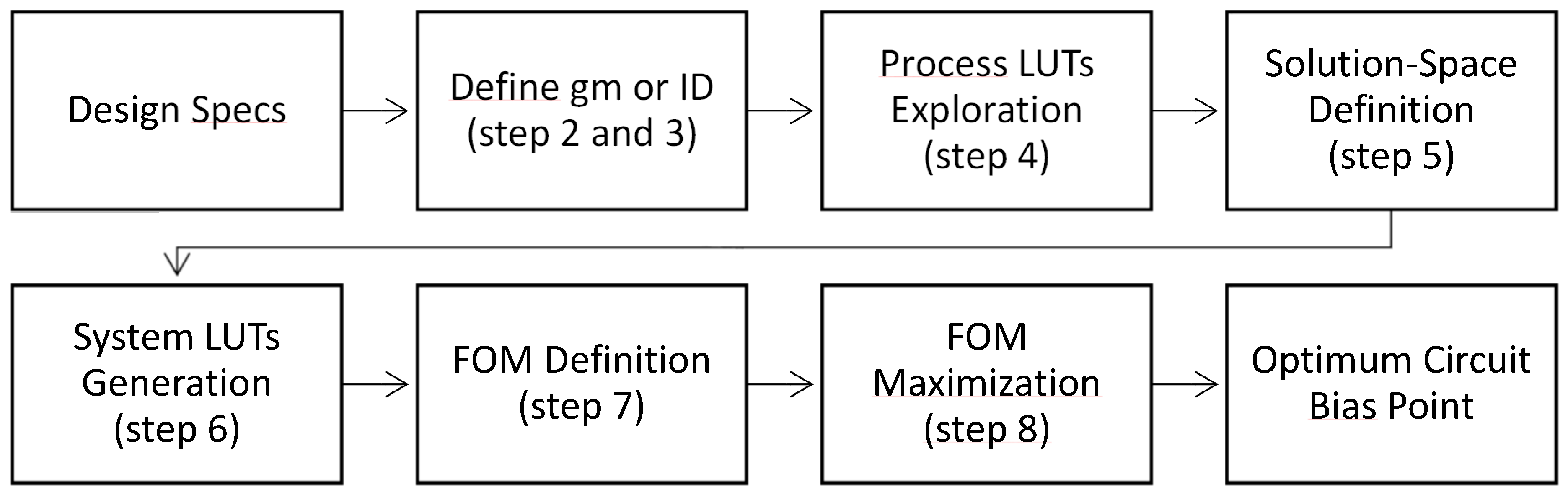
D of the two stages. The proposed algorithm is composed of the eight steps represented in
Figure 4.
Step 1. To be able to run the framework, we must, first of all, generate Jespers and Murmann’s lookup tables (LUTs) for the MOS transistors of the 0.13 µm process used to design the circuit (these LUTs are denoted in
Figure 4 with the name “process LUTs”). A graphical view of these lookup tables is provided in
Figure 3.
Step 2. Given the desired design specs. (i.e., gain and load resistance), Equation (6) can be used to derive the value of gm.
Step 3. Once the value of gm is found, the algorithm sweeps gm/ID in the whole feasible range (i.e., from 5 S/A to 25 S/A) and computes the associated currents ID(SS) and ID(TS).
Step 4. Given Jesper and Murmann’s lookup table of the current density (I
D/W vs. g
m/I
D) the algorithm extracts W
(SS) and W
(TS) for all values of g
m/I
D explored. To maximize the speed of the mixer the length L of all transistors is set to the minimum value (130 nm) allowed by the technology used to implement the circuit [
20,
21].
Step 5. The algorithm performs a systematic analysis of the mixer’s performances. For each bias point it computes the DC-power consumption, it checks that all transistors operate in saturation and it prunes any unfeasible solution.
Step 6. For each point that represents a feasible solution, the algorithm computes the gain of the mixer and then discards any point that exhibits a gain that does not meet the specifications. This procedure is repeated for the noise figure and the third-order intercept of the mixer. The system performance metrics computed in this step are captured and stored in the form of lookup tables (these LUTs are denoted in
Figure 4 with the name “system LUTs”).
Step 7. Given the solution space computed in the last step, to compute the best bias point of the circuit, an overall figure of merit (FOM) is introduced.
Step 8. The algorithm returns the best circuit bias point to be used to design the down-conversion mixer, by looking up the solution (i.e., the value of gm/ID) corresponding the maximum value of the FOM.
Several performance metrics can be used to define the FOM of the circuit. The designer can choose the one he prefers without performing any software modification. In facts, the algorithm computes the FOM value by simply exploring the lookup tables related to the system performance (conversion gain, noise figure, and so on). In our design, to obtain the best balance between the various parameters specified, we defined the following figure of merit (FOM):
where G is the gain, IIP3 is the input third-order intercept, NF is the average noise figure and P
DC is the power dissipation. The definition of the FOM is up to the designer and it is based on the target application of the mixer. Once the lookup tables for the performance metrics of the system (gain, noise figure, etc.) are generated the designer select the figure of merit as a function of the relative importance of the various performance metrics.
4. Results
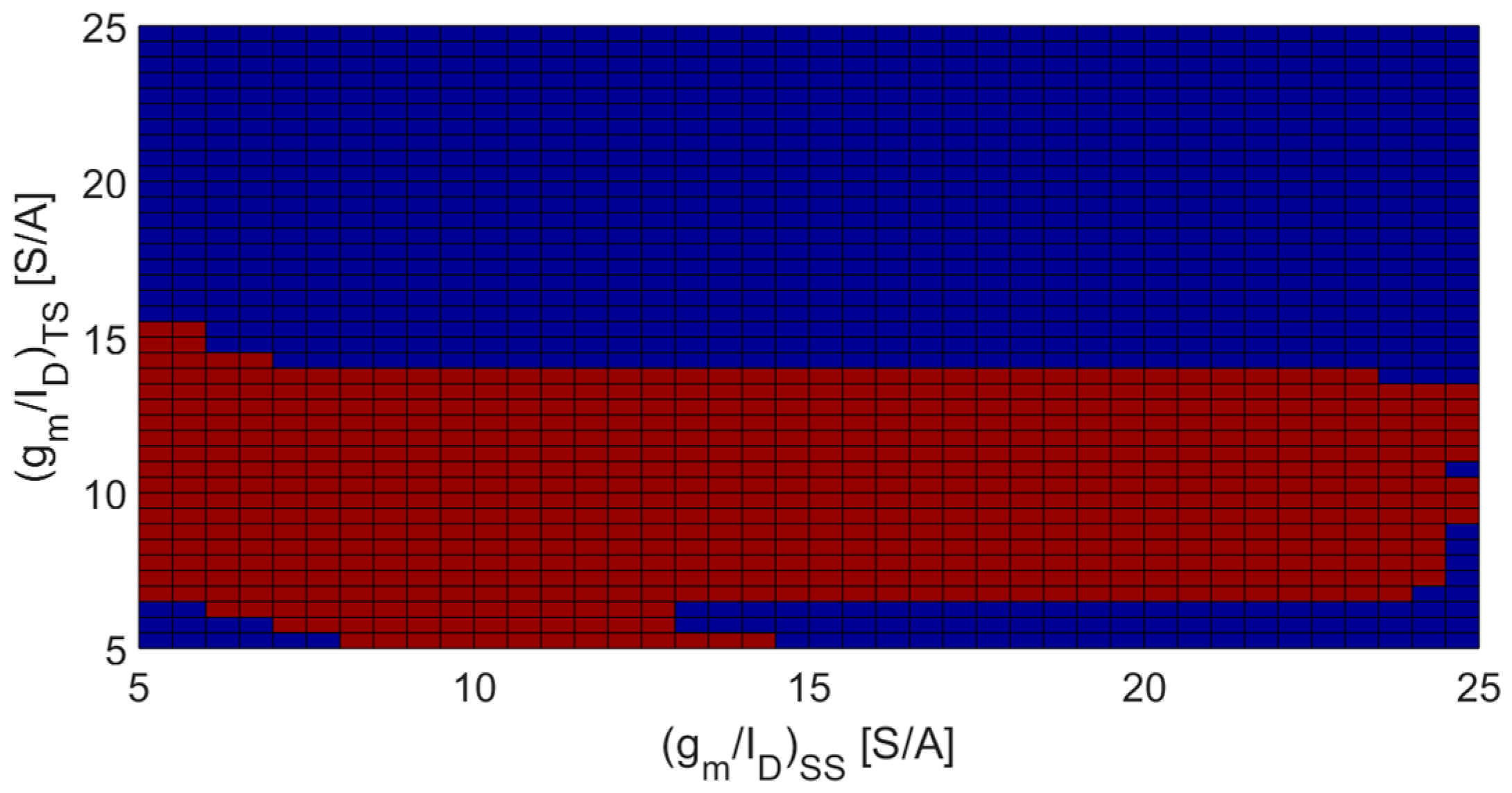
The supply current drained by the mixer should be of less than 2 mA with a 1.5 V voltage. The desired gain had to be greater than 10 dB with a load of 500 Ohms, and the IIP3 had to be better than −5 dB. The circuit performances were validated for a LO sine wave with a frequency of 5.7 GHz and a maximum power of 0 dBm.
Figure 5 summarizes the feasible solutions (red color) obtained by the algorithm. From this figure, it is possible to observe that the transistors in the transconductance stage (TS) should be biased with a g
m/I
D between 5 S/A and 13 S/A while the transistors in the switching stage (SS) can be biased at any g
m/I
D level.
Figure 6a provides the curve characterizing the input third-order intercept of the mixer. Given that the MOSFETs in the switching state must be biased with a g
m/I
D in the range between 5 S/A and 10 S/A, we note that as the bias point of the transistors in the transconductance stage passes from strong to weak inversion, the IIP3 decays linearly. Moreover, we note that biasing the transistors of the switching stage in weak inversion, the IIP3 behavior can be approximated by a parabolic function with a local maximum for g
m/I
D(SS) of 20 S/A. The IIP3 curve has been computed using two tones, one at 5.8 GHz and the other one at 5.85 GHz.
Figure 6b sketches the curve characterizing the average noise figure of the mixer. The average is taken over the ultra-wide bandwidth (UWB) frequencies range (3.1 ÷ 10.6 GHz). Imposing that the SS transistors are biased in strong inversion, we note that as the transistors in the TS pass from strong to moderate inversion the noise figure decreases exponentially and approaches a value that is less than 12 dB. The curve illustrating the mixer gain is reported in
Figure 6c. The gain in the mixer can be approximated by a parabolic function in both g
m/I
D directions. Biasing the transistors of both stages in moderate inversion, the mixer exhibits an absolute maximum gain of 13.5 dB.
Figure 6d shows the mixer’s power consumption. As expected from the circuit analysis of the mixer [
4], the power dissipation of the transconductance stage is dominant over the power dissipation of the switching stage. From
Figure 6, we note that the power is approximately constant along the SS axis, while along the TS axis it exhibits an exponential roll-off as g
m/I
D increases.
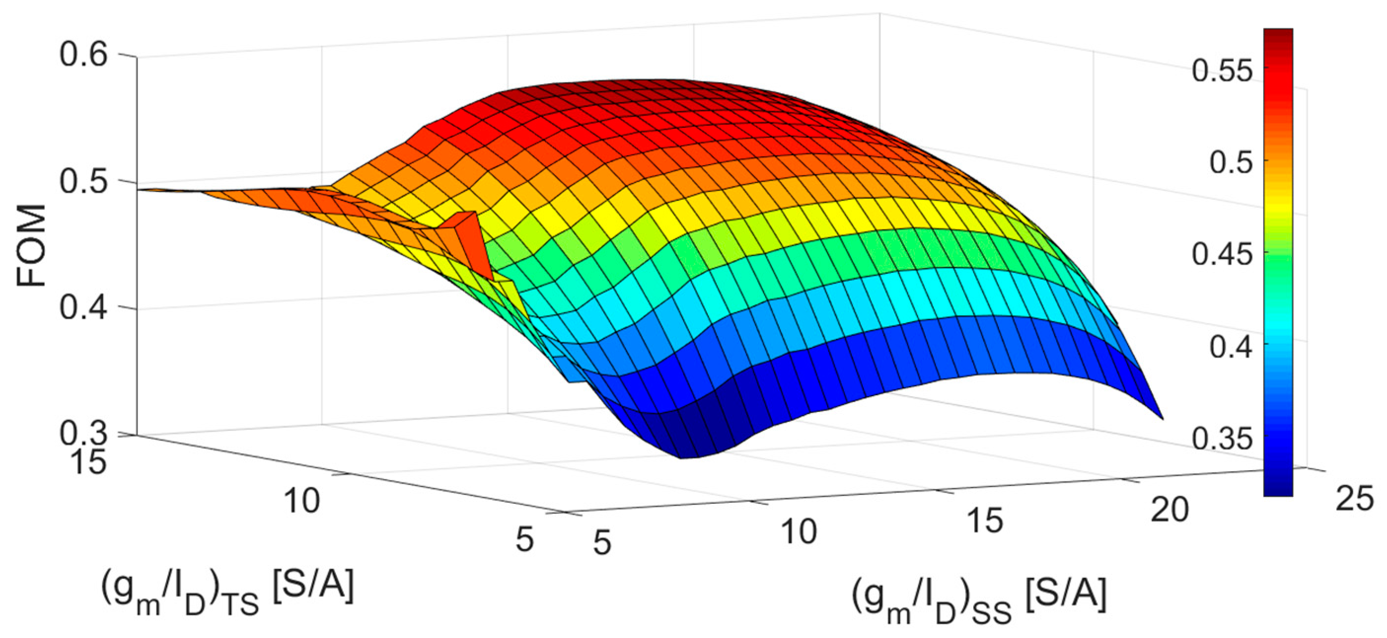
Finally, the FOM as a function of g
m/I
D(TS) and g
m/I
D(SS) ratios is presented in
Figure 7. Note that the FOM presents a local maximum when biasing the TS in moderate inversion and the SS between moderate and weak inversion.
The algorithm returns as an optimal solution the FOM corresponding to gm/ID(SS) = 18 S/A and gm/ID(TS) = 10.5 S/A. The jittery nature of the FOM curve is a result of the irregular behavior of both the IIP3 and the noise figure. To avoid this problem, the FOM can be re-defined introducing weighting coefficients in the formula. The introduction of weighting coefficients also allows the designer to drive the optimization process to favor one or more performances based on the target application. For example, in the case of the mobile market, power consumption is more critical than IIP3 and so it is possible to introduce a coefficient in the FOM expression that induces the algorithm to maximize power performance more than other performances.
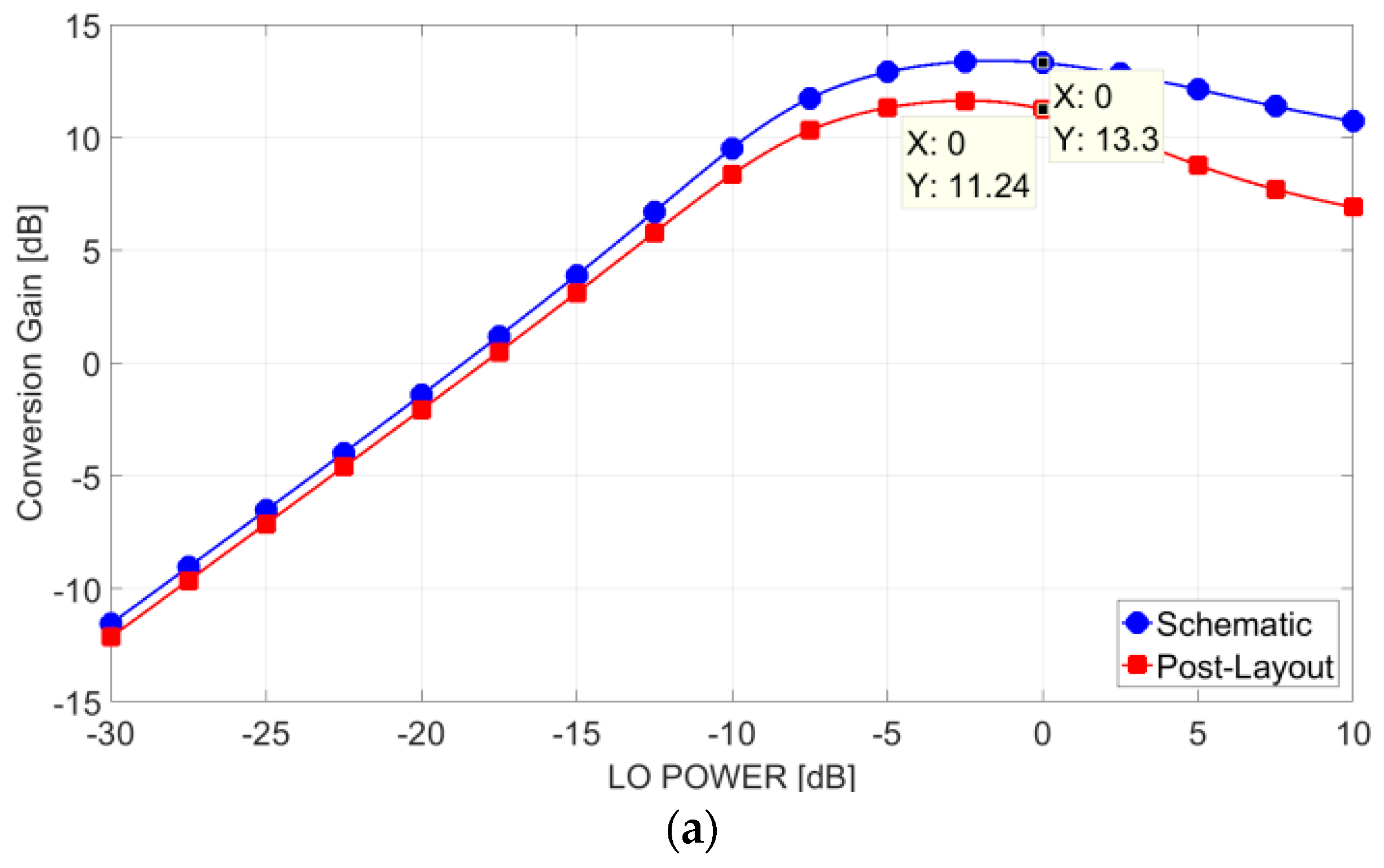
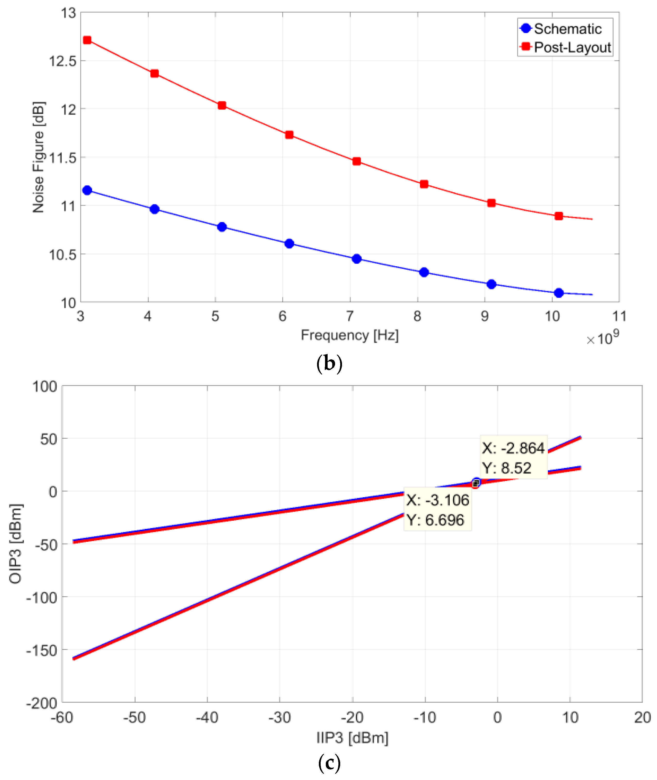
Figure 8 reports the post layout performances of the double-balanced mixer designed with the proposed method. With a LO power of 0 dBm, the post-layout mixer gain is about 11 dB. This corresponds to a loss of about 2 dB compared with the theoretical gain expected. The main reason lies in the parasitics introduced by the bias current source physical implementation. Similarly, the post-layout IIP3 is −3.1 dBm lower than the ideal value of 2.8 dBm. In terms of power dissipation, with a voltage supply of 1.5V, the mixer-core consumes only 2.1 mW. Although the performance in post-layout simulations are worse than the theoretical values expected, they still exceed the design specification and therefore validate the proposed design approach.
To assess the quality of our design we compared its performances with the performances of other CMOS Gilbert mixers found in literature. Using the proposed approach (see
Table 1) our mixer achieves the best (post-layout simulation) FOM. Unfortunately, since not all references state unequivocally whether their figures come from measurements or simulation, a fair comparison is problematic. This result is obtained using a traditional double-balanced circuit architecture and did not require the introduction of any of the dedicated topological improvements that can be found in literature. Nevertheless, the proposed approach is completely general and if desired it can be easily extended to other circuit architectures that have the potential to improve a mixer performance. The final layout of the mixer’s core is sketched in
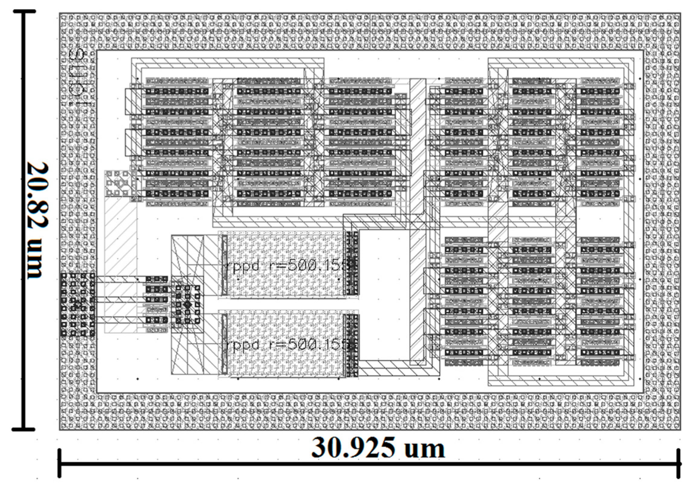
Figure 9. The mixer-core measures less than 21 µm by 31 µm (bonding pads and baluns excluded).


