1. Introduction
Dielectric permittivity plays a fundamental role in describing the interaction of electromagnetic waves with matter. The boundary conditions, wave propagation in matter, and wave reflection/transmission on interfaces all involve this parameter. In practical applications, the processes of link budget (wave attenuation), channel characterization (wave dispersion), and multi-path effect (reflection/transmission) are representative examples of wave interaction with media [
1]. Understanding these phenomena is a fundamental requirement in communication system design.
With the rising of millimeter wave technology, for example, 5G communication [
2], millimeter wave radar and sensing [
3], accurate characterization of electronic materials for these applications is of fundamental significance. Although the dielectric properties have been widely investigated in the microwave range or below, the work in the millimeter wave range is much less thorough. The reason is that it has been a long period that the operation frequency of communication systems has been limited to the low frequency range [
4]. However, problems such as frequency shift and increased insertion loss are often observed in the millimeter wave circuit design due to inaccurate permittivity [
5]. In view of these facts, it is necessary to investigate the dielectric property of materials in the millimeter wave range. Particularly, we restricted our study in the E-band (60–90 GHz), mainly due to the fact that many applications fall in the range, such as the planned unlicensed 64–71 GHz band for 5G communication in the USA [
6] and 77 GHz vehicle radar [
7]. In addition, we selected silicon as the representative materials for measurement since it is one of the most important semiconductor materials in electronic systems.
There are many publications focused on the complex permittivity of silicon [
8,
9,
10,
11,
12,
13,
14,
15,
16,
17]. Reference [
8] used a capacitive method, which was suitable for measurement in low frequency range. Reference [
9] investigated the n-type silicon at 107.3 GHz using a non-focusing free-space system. Afsar and his colleagues [
10,
11] measured several semiconductor samples using dispersive Fourier transform spectroscopy (DFTS) and presented data over 100–450 GHz [
10,
11]. It was found that the permittivity slightly increased with frequency from 100 to 180 GHz and then decreased with frequency. In contrast, the loss tangent decreased with the frequency monotonically. However, for silicon of resistivity 11,000 Ω·cm, the loss tangent increases with frequency (see Figure 3 in Reference [
11]). The Fabry–Perot resonator was also utilized for silicon characterization over the frequency range of 30–300 GHz [
12]. Additionally, it was found that the permittivity had a slight tendency of linear decreasing over the frequency range. An extensive investigation was conducted by Krupka and his colleagues [
12,
13,
14,
15,
16]. These measurements used resonator techniques at various frequency ranges below 50 GHz. It was demonstrated that the loss tangent decreased with increasing frequency, and in most cases on the order of
. Temperature effects were also systematically investigated over the range of 10–370 K. The real part showed very stable properties over the investigated frequency and temperature ranges, in the worst case in the range of 11.46–11.71. These findings provide valuable reference to the permittivity of silicon.
In these studies the E-band is covered in [
12], where it was stated that the refractive index decreased linearly with frequency. Although it is in a small magnitude, such a statement is slightly different from other publications. Considering that many applications have been developed in the E-band, it is best to conduct the measurement in this band. In consideration of these facts, this paper introduces a broadband method for dielectric measurement on semiconductor materials, with measurement conducted on undoped silicon. A detailed description on the condition of creating quasi-plane wave is given. Plane wave is very desirable in free space measurement. The retrieval of the permittivity incorporates the theories of wave propagation and scattering parameters. Temperature dependent characteristics are examined at 20, 25, and 30 °C.
The remaining parts are organized as follows:
Section 2 is devoted to a general description on the permittivity and measurement techniques;
Section 3 describes the method generating a quasi-plane wave;
Section 4 is the retrieval method and
Section 5 is the measurement results; the last part
Section 6 concludes this work.
2. Permittivity and Measurement Techniques
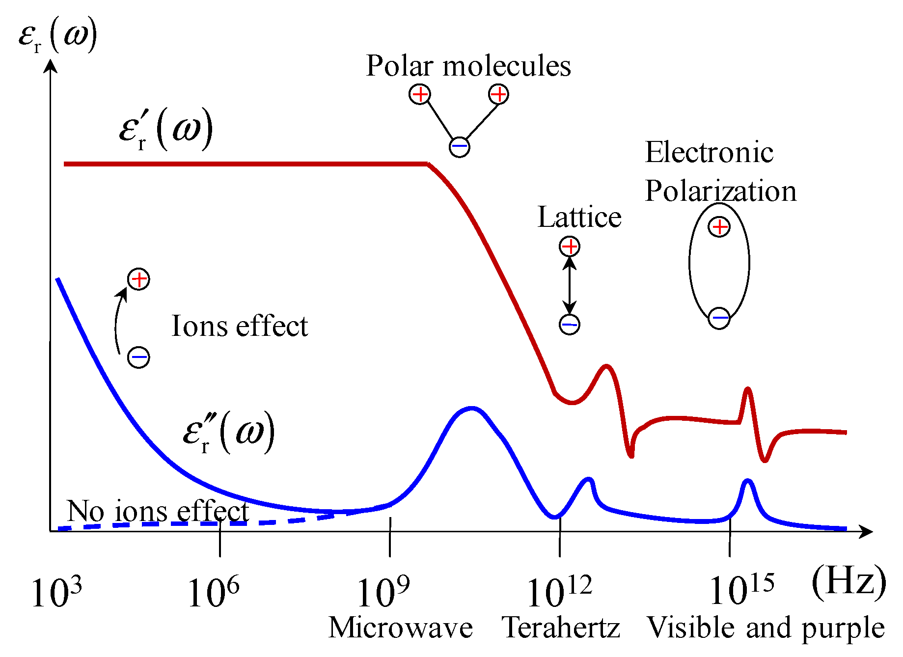
Dielectric permittivity is a macroscopic description of many microscopic processes, such as dipole relaxation, lattice vibration, and electronic polarization. These processes take effect at different characteristic frequency ranges, as illustrated in
Figure 1.
The permittivity is actually a complex quantity. The imaginary part is due to dielectric loss. One representative mechanism of loss is the dipole relaxation [
1]. When a dipole tries to follow the alternating electric field, friction between dipoles would cause loss of energy. Other mechanisms include conductive loss and lattice loss. These mechanisms can be incorporated into a single parameter the complex permittivity
where the real part is the relative permittivity and the imaginary part is referred to as the loss factor. Since these mechanisms fall in different frequency ranges, the permittivity exhibits a dependency on frequency
Referring back to
Figure 1, it has to be noted that the ticks on the axes are not to exact scale, only for illustrative purposes.
Methods of dielectric measurement shall vary with frequency due to the frequency dependent and electrical size effects. Several methods can be used for dielectric measurement in the millimeter wave range, such as resonator method, transmission line method, and free space method [
18]. The resonator technique is an efficient way for low-loss single frequency measurement. The transmission line method imposes considerable challenge on sample preparation with the increase of frequency. Therefore, the free space system is more preferred for measurement spanning over a whole frequency band.
Free space measurement requires ideally a plane wave system. However, plane wave is merely an ideal model that can be approximated using the far field of an antenna, but the far field would require a space too large to use. Alternatively, we used a quasi-optical (QO) system to create a quasi-plane wave for dielectric measurement. The QO technique is particularly suitable for millimeter wave system due to its low-loss and wideband nature. It is also possible for multi-polarization measurement. In addition, the size of a QO system is controllable.
3. Generating Quasi-Plan Wave
The QO technique was originally developed for radio astronomy for low-loss and wideband receivers [
19]. Transferring the QO technique to dielectric measurement is a good attempt. The QO theory is based on Gaussian beam description of an electromagnetic wave. The propagation and refocusing of a Gaussian beam are illustrated in
Figure 2. A Gaussian beam can be described using [
20]
where
is the beam waist located at
,
is the beam radius,
is the radius of curvature and
is the phase shift. These parameters can be written as
It is seen from Equation (4) that the radius of curvature of the wave front is infinite at the beam waist. This is a property of plane wave. However, as the beam propagates, the size of the beam increases with the propagation distance due to the diffraction effect of the electromagnetic wave, gradually forming a spherical wave front. Therefore, a focusing unit has to be used to refocus the beam to a beam waist. The beam transformation by a focusing unit can be analyzed using the ABCD matrix.
In a general case, the transform by a focusing unit of focal length
f can be calculated by
where
,
,
, and
are the input distance, output distance, input beam waist, and output beam waist, respectively. Additionally,
is the confocal distance
It is seen that given , the output distance is always f, independent of the working frequency. Such a feature enables broadband operation.
For a special case, if two identical focusing units are used and placed 2
f apart, i.e.,
and
(see
Figure 2), the output beam waist will be the same as the input beam waist
. Therefore, the transmitting and receiving horns can be fabricated to be the same. Such a special case gives one a symmetrical structure and is referred to as Gaussian telescope. The system in this paper is in the form of Gaussian telescope.
For a free space system, low cross polarization, low transmission loss, low reflection, and good bandwidth are preferred. To meet these requirements, metallic reflectors can be used as focusing units. Although a dielectric lens can also be used for focusing, the inherent reflection loss and dielectric loss as well as its narrower bandwidth make it less preferred. To obtain low cross polarization, a high-quality horn antenna is always plausible. Corrugated horns are good candidates to the transmitting/receiving units since good bandwidth and polarization purity can be achieved [
21]. In addition, the system has to be capable of creating a local plane wave with acceptable transverse size. Additionally, the field should be close enough to a plane wave over a longitudinal distance to ensure that thick samples can also be measured. Such requirements may demand the reflector to be a paraboloidal surface. However, the ellipsoidal surface is more common in a QO system [
20].
Considering these requirements, the following parameters were used for the system design (see
Table 1). Parameters
R1,
R2, and
θ are illustrated in
Figure 3a, and
f is the equivalent focal length of M1 and M2
The parameter
w is the beam radius along propagation, as indicated in
Figure 3b.
The fabricated system is shown in
Figure 3a, and the beam radius (solid curves) and wave front (dashed curves) are plotted in
Figure 3b. The beam radius at the location of M1/M2 is 33.19 mm, which requires the reflector to be 132.76 mm (4
w criterion) in length. To accommodate lower frequency of the E-band, the size of the reflector is fabricated to be 200 mm. At the location of the sample, the beam radius is 32.15 mm, which requires the reflector to be 128.60 mm in length. Again, the length of the sample would be suggested to be 200 mm for low frequency consideration.
The dashed lines in
Figure 3b are calculated wave fronts using a computer program based on Equation (5). Noticeably, the wave front between M1 and M2 is very close to a plane wave. This is a very good property for dielectric measurement since phase error will be minimized. It is calculated that the phase difference between the edge of the reflector to that of the on-axis phase is only within 10°. The extenders are
VDI VNAX standard, working at waveguide band WR-12, corresponding to 60–90 GHz. The horns are corrugated ones launching Gaussian beams. The Gaussianities of the horns are obtained by calculating the power coupling between an ideal Gaussian beam and the measured results, giving 98.5%.
4. Retrieval Model
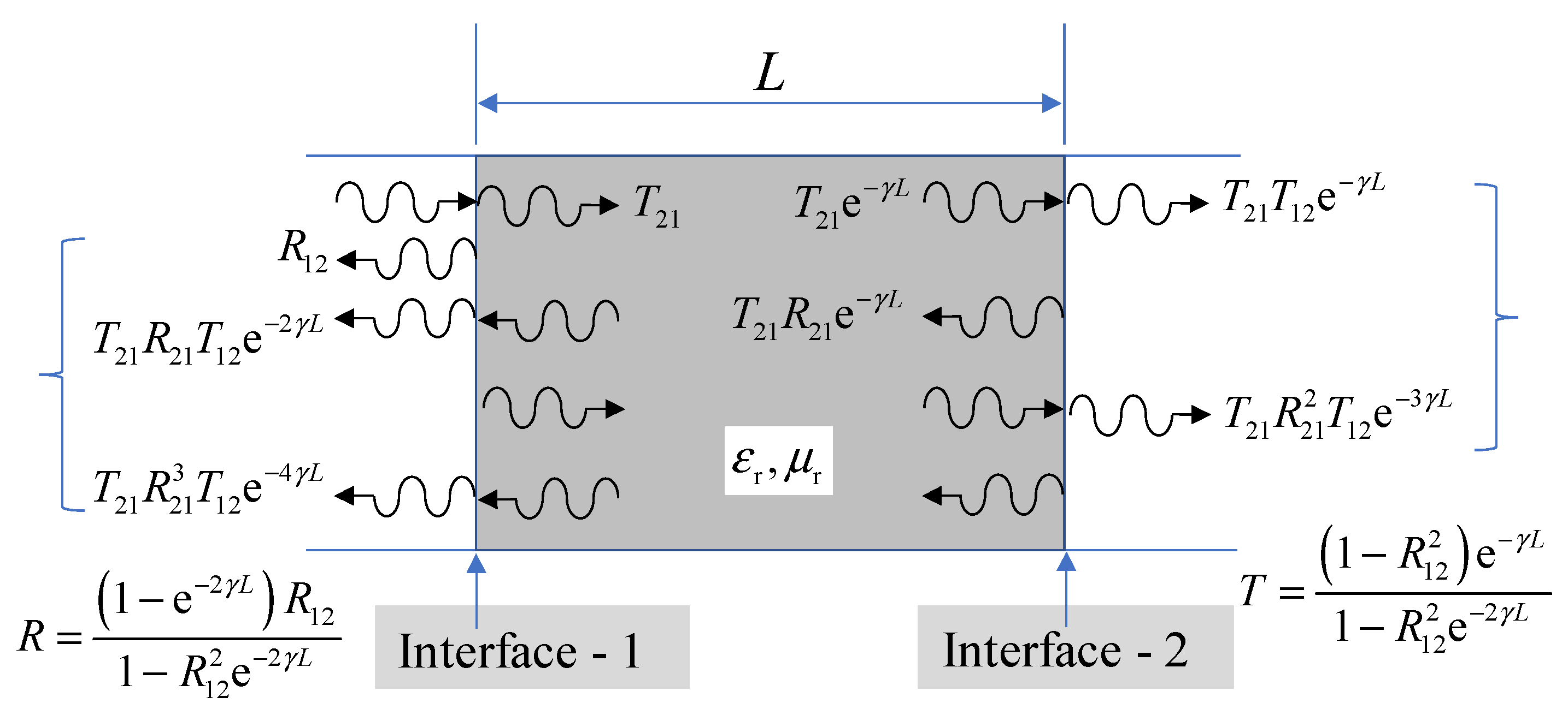
Since we created a quasi-plane wave, the analysis can be conducted using the plane wave method. Such assumption would introduce limited measurement error while significantly reducing the complexity of mathematic manipulation. Reflection on an air-medium interface is an important part in electromagnetism. The reflection model, however, is based on an ideal case where the medium is infinitely long. To apply the ideal model to dielectric measurement, a more precise model has to be built based on the ideal model. This can be simply done by introducing a second interface. The structure can be described by an air-interface-medium-interface-air model, as illustrated in
Figure 4.
The interaction of the electromagnetic wave with matter on interfaces 1 and 2 is actually the same as the ideal model. Differently, the reflected wave inside the medium will bounce forward and back. Additionally, these multi-reflection/transmission effects have to be included in calculating the total reflection and transmission coefficients. Using the same mathematical manipulation of [
22], the total reflection and transmission coefficients were found to be
where the reflection of a plane wave on interface 1 is
and the wave propagation coefficient is
Such a structure is identical to a two-port microwave network, where the elements of S11, S21 are the reflection and transmission coefficients of port 1, and S22, S12 are the reflection and transmission coefficients of port 1, respectively. Interface 1 and interface 2 are similar to port 1 and port 2 of a two-port microwave network, so that the scattering parameters S11 and S21 measured using a vector network analyzer (VNA) can be correlated to the reflection and transmission coefficients, respectively. To correlate the transmission coefficient to S21, a measurement on open air has to be conducted prior to sample measurement. In comparison, to correlate the reflection coefficient to S11, a reference measurement of planar metallic plate has to be used. To this end, a link between the wave propagation in a sample and the scattering parameters measured by a vector network analyzer was established.
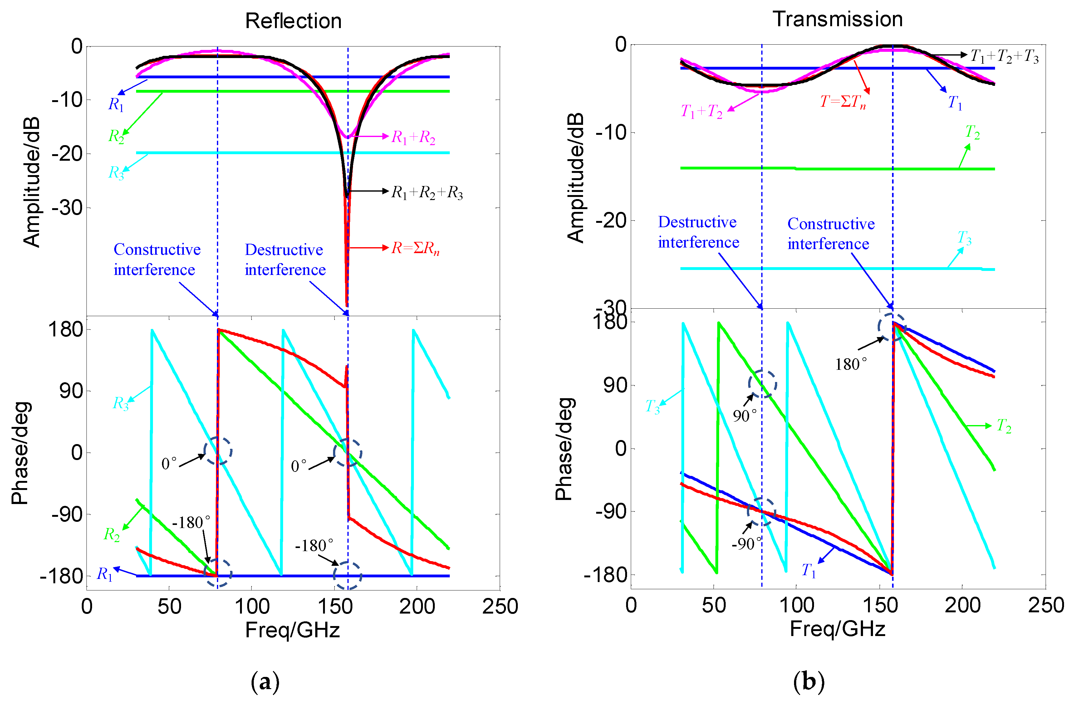
In
Figure 5, we present the first few terms in comparison to the total reflection/transmission coefficients to examine the wave interference at different frequencies. It is seen that the first two or three terms make up most of the reflection/transmission. It is also found that at 160 GHz, the first reflection R1 has a phase of −180°, while the second term R2 and the third term R3 are 0° in phase. Therefore, a destructive interference is formed. At 80 GHz, a constructive interference is formed. Although the third term is out of phase with the first term, the amplitude of R3 is 13 dB smaller than R1, therefore, it would not contribute too much to the interference. The constructive point of the reflection is the destructive point of transmission and vice versa.
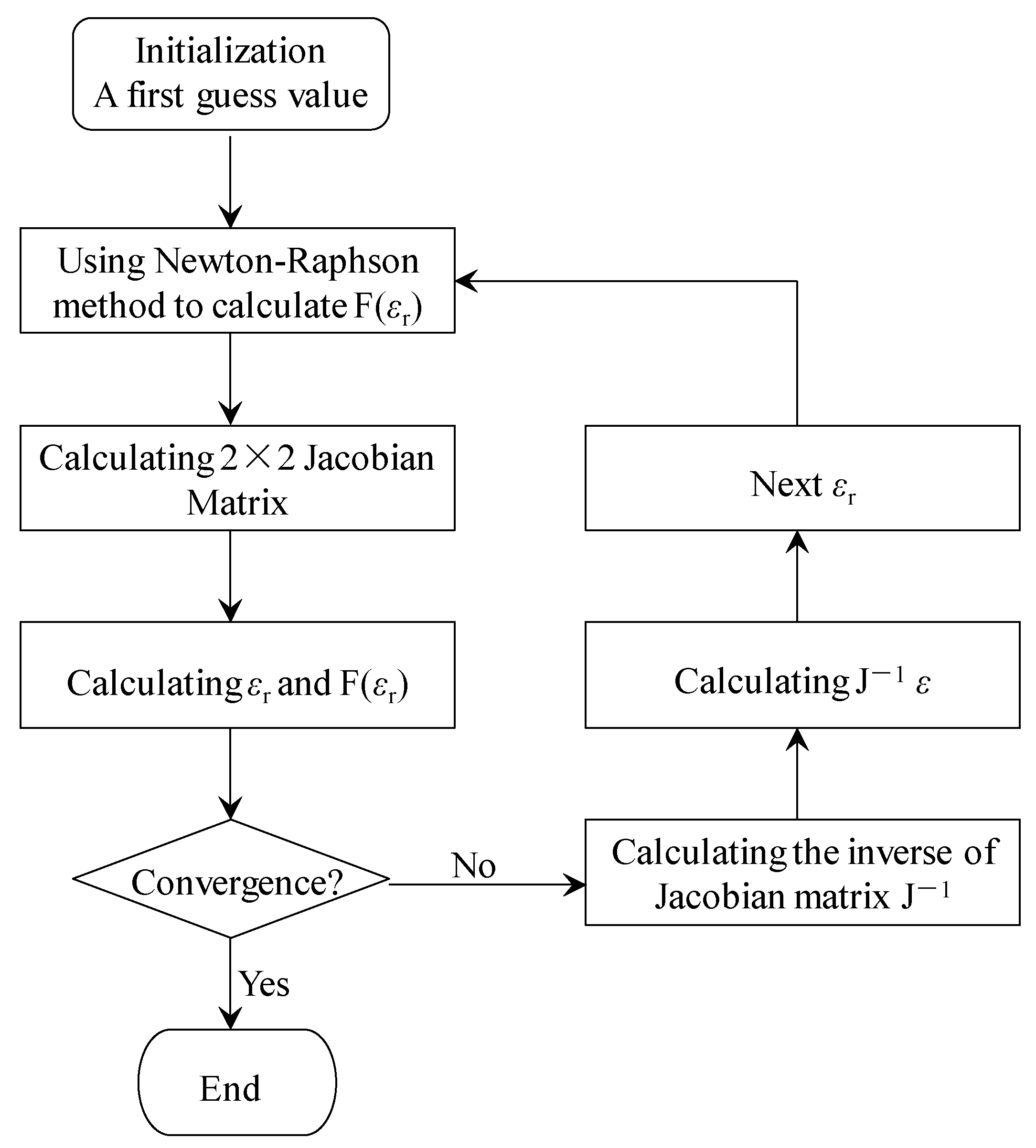
Retrieve of dielectric permittivity can be fulfilled using Equation (10). For non-magnetic materials, a simple mathematic manipulation can be employed as shown in Reference [
23]. The error function can be defined as
Or using a weighted error function
These numerical techniques are available in the literature [
22]. In this work, Equation (13) was used as the error function. A flow chart of the Newton–Raphson method for numerical solving is shown in
Figure 6.
5. Experiment and Results
The undoped silicon wafer was used for representative measurement. Silicon is a very common material in semiconductor circuits. The provided value of resistivity is 70 kΩ·cm. The diameter of the wafer is 300 mm and the thickness is 660 ± 10 μm. Such a size is sufficiently large for measurement. Both sides of the silicon wafer were polished. Measurement was conducted at 25 °C. The measurement was first conducted on open air. Such a measurement was to remove the background effects, including atmospherical absorption. However, since the atmospherical absorption in the E-band is less than 16 dB/km according to the ITU standard (ITURP.676-11-201609), the total attenuation due to air is less than 0.03 dB given that the path length of this system is smaller than 2 m. In addition, the reference measurement will introduce a phase difference of
, which should be subtracted from the resulting phase. The corrected raw data of S21 are plotted in
Figure 7. It is seen that the transmission response is close to a sinusoidal function. To eliminate the noise, the third and fifth order polynomial fittings were used. Using the Tailor expansion, it is found
If the fifth order polynomial fitting was used, the difference to the third order is only 0.14 dB in the worst case, and the phase difference is only 1°, as shown in
Figure 7. The seventh order can also be used, but no significant difference was observed. This is a piece of evidence that the fifth order fitting provides adequate accuracy.
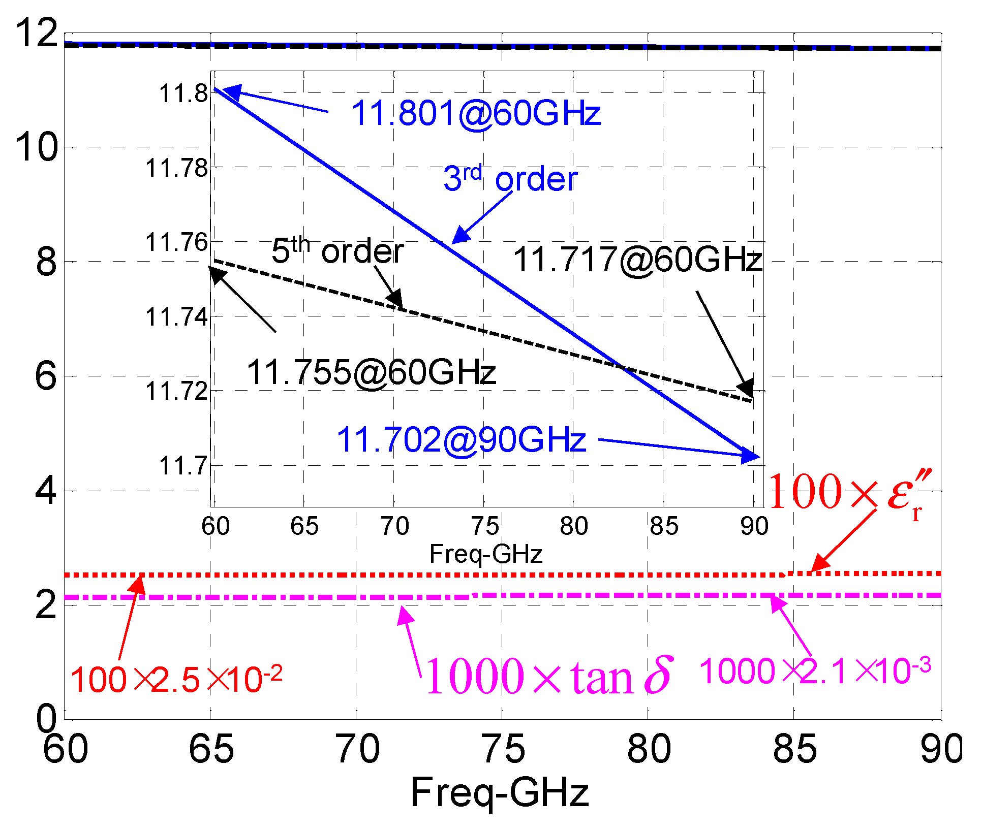
The fitting data were used for permittivity retrieve. In addition, the permittivity versus the frequency is plotted in
Figure 8. The real part is plotted in solid line, the imaginary part is plotted in dotted line, and the loss tangent is plotted in dash-dot line. The imaginary part is scaled by 100 and the loss tangent is scaled by 1000.
It is seen that the real part of the permittivity is 11.801 at 60 GHz and gradually decreases to 11.702 at 90 GHz for the third order fitting. For the fifth order fitting, it is 11.755 at 60 GHz and slightly changes to 11.717. The difference of the third order and fifth order fitting is about 0.5%. Such results are in line with the published data of 11.74 [
12], and is slightly smaller than the provided value of 11.9 at 1 MHz. The loss tangent of the intrinsic silicon is on the order of 10
−3, showing not too much difference between the third and fifth order fitting. However, it has to be mentioned that being constrained by the accuracy of the free space method on the loss factor, it is one order larger than the results in References [
14,
15,
16]. It is probably due to this reason that the tendency of loss factor with frequency was not exhibited.
To examine the uncertainty due to the magnitude and phase, we followed the error model in Reference [
22], (see Equations (27)–(37) in Section III). The magnitude stability of the
VDI modules is 0.10 dB, and the phase stability would be 5°. In addition, the fitting model may introduce an extra 0.10 dB magnitude error and 1° phase error. Feeding these values into the error model would give a maximal uncertainty of 5%, and an average error of 3% can be expected.
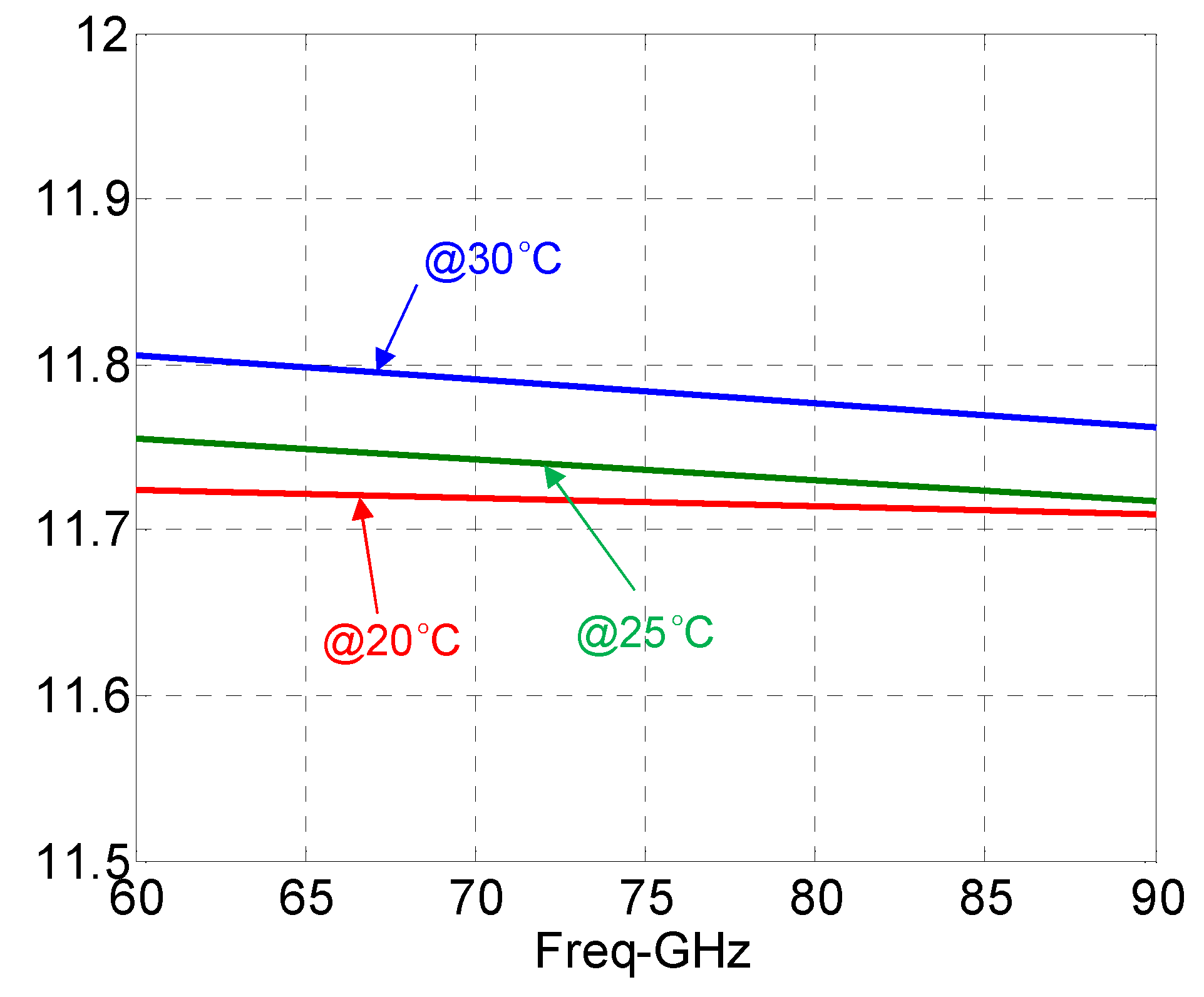
To investigate the temperature dependent nature of undoped silicon, the temperature was set to 20, 25, and 30 °C. The test bench was placed in a temperature controllable room. The temperature around the sample was measured using a Fiber Optical Sensor (
OMEGA FOB-102), with the sensitivity of ±0.1 °C. Using the same procedure and taking the fifth order fitting, the retrieved data are plotted in
Figure 9. There is a tendency for the real part to decrease with frequency, though not noticeably. It is also found that with the increase in temperature, the real part tends to increase with the increase of temperature. This is in line with the results of References [
13,
15], where a more broadband temperature range was considered. However, it has to be mentioned that the variation of the permittivity with frequency and temperature is very small, and the overall variation is within 11.75 ± 0.06. It implies that the undoped silicon has a very good temperature property, or very small temperature coefficient. This is a very preferential property for electronic systems.
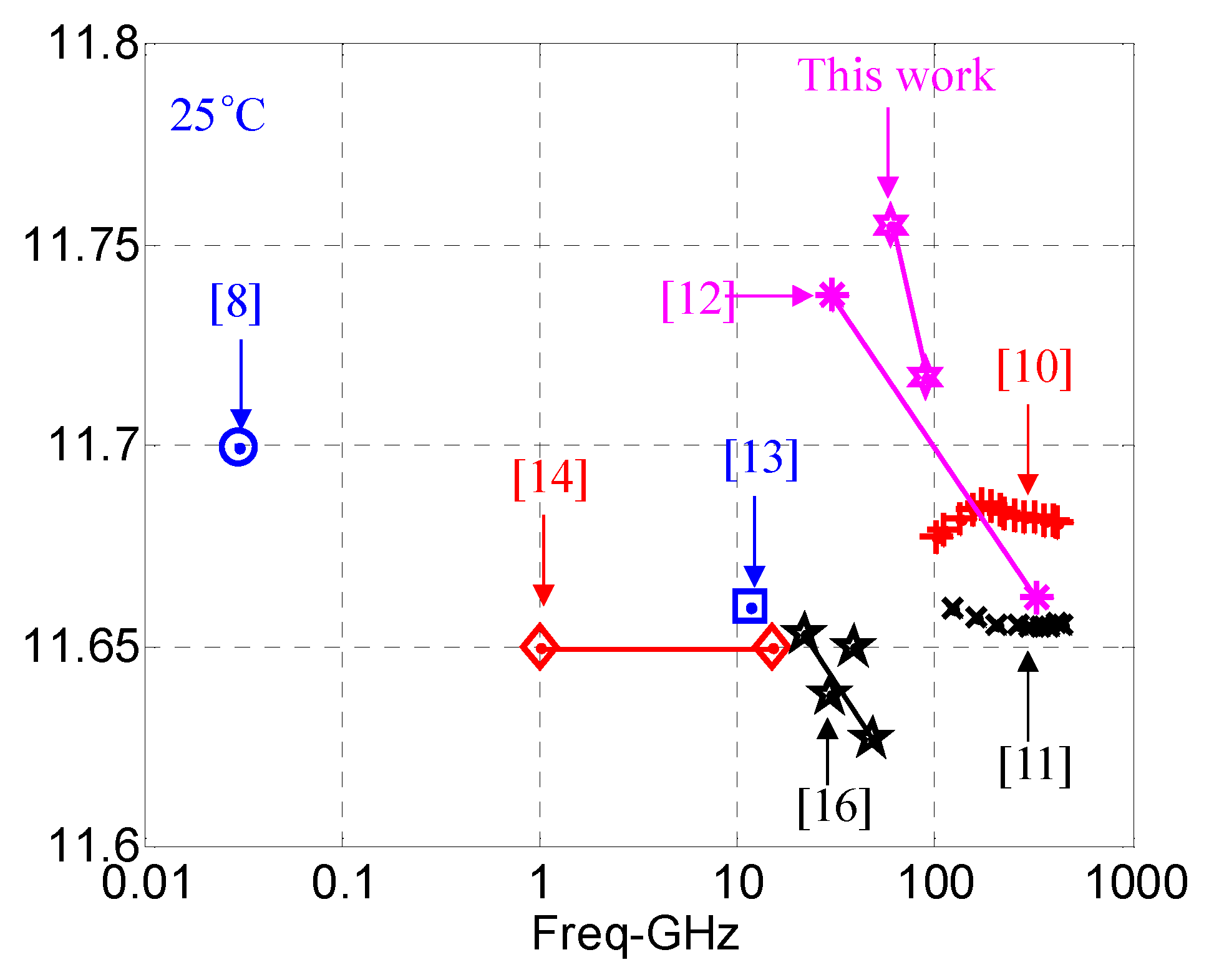
A comparison of this work and the published work is shown in
Table 2. The extracted data at 25 °C are plotted in comparison in
Figure 10. It is noted that as the silicon samples used are from different vendors, differences in resistivity may exist. However, it is seen that the measured results from different groups are in the range of 11.63–11.76, showing a discrepancy of ±0.6%. The measured results in this work are in agreement with the results in the literature [
10,
11,
12,
13,
14], within a discrepancy of 1.0%. It is also seen that the variation of the permittivity of silicon is very small below 450 GHz. In view of this fact, the dispersion of silicon is very weak, if there is any.


