1. Introduction
The electromagnetic detection method has the advantages of deep exploration depth, high horizontal resolution, strong penetration capability and anti-interference, and has been widely used in geophysical exploration such as mineral exploration, water resources exploration and engineering geological survey [
1,
2,
3,
4]. The research of the excitation source is an important topic in geoscientific instrument research. However, in most power supply situations, there are large inductive loads, small loop resistance, low power supply voltage, etc. Therefore, it is very difficult to obtain ideal high-frequency AC square wave current source.
The linearity of the commutation edge, short commutation time, high stability are important characteristics of the pulse current source, and also the core problems for researchers. When the turn-off time is constant, increasing the voltage pulse amplitude can improve the linearity of the current falling edge and improve the waveform quality. Based on the idea of high voltage clamping, [
5,
6] proposed a method to control the turn-off time and improve the slope of the front and rear edges of the current by adjusting the voltage of the clamping voltage source. In [
7], the solid-state DC/DC boost front-end and h-bridge output are used to achieve the purpose of rapid current rise. In order to realize the output current steep pulse, literatures [
8] and [
9] respectively put forward the method of using high-voltage dc power supply and increasing boost charging circuit to charge capacitor during pulse current commutation. In order to improve the quality stability of transmitting current waveform, a method for suppressing the ripple current of the flat-top section of the emission current by introducing a passive bypass circuit in [
10], and reference [
11] proposed a high precision mixed-signal (analog and digital) plan for output current stabilization. A model predictive current control scheme with phase-shifted pulse-width modulation is introduced in [
12], which has the advantages of small tracking error and high steady-state performance. What’s more, reference [
13] proposed a high-precision pulse current source control system can get good dynamic response by improving switching characteristics, and the flat top current can be regulated with precisely defined precision. A converter based on switched-capacitor units with high voltage gain and high efficiency was proposed in [
14], the proposed topology can generate repetitive high-voltage pulses. The literature [
13] proposed a pulse current source control system with high-precision and fast dynamic response through the improvement of control strategy and algorithm.
Recently, due to the need for engineering geophysical prospecting, detection of geological information in the shallow layer and the superficial layer of the ground has received a great deal of attention [
15,
16], this requires the transmitter to have a higher frequency of current. The frequency domain electromagnetic transmitter needs to solve the problems of fast commutation of current, high linearity of commutation, wide frequency transmission (500 Hz ~ 100 KHz) and constant current amplitude. For the key technical problems of frequency domain electromagnetic transmitter, this paper proposes bipolar broadband communication pulse current source circuit, the highest transmission frequency can reach 100 KHz, the maximum emission current is 15 A, the current rises rapidly to the set value with the slope of 10
7 A/s, the current is quickly turned off from the positive polarity amplitude to the negative polarity amplitude, and there is no dead-time in the middle, it can maintain the current value at 15 A in the flat stage, which achieves wide-band constant amplitude and the current amplitude is greatly improved at high frequencies. The proposed approach provides a solution to the high frequency and high current emission problems encountered in frequency domain transmission systems.
2. Magnetic Source Frequency Domain Electromagnetic Transmitter
This section describes the schematic, operation principle, and realization details of the proposed magnetic source FEM probing circuit.
2.1. Operation Principle
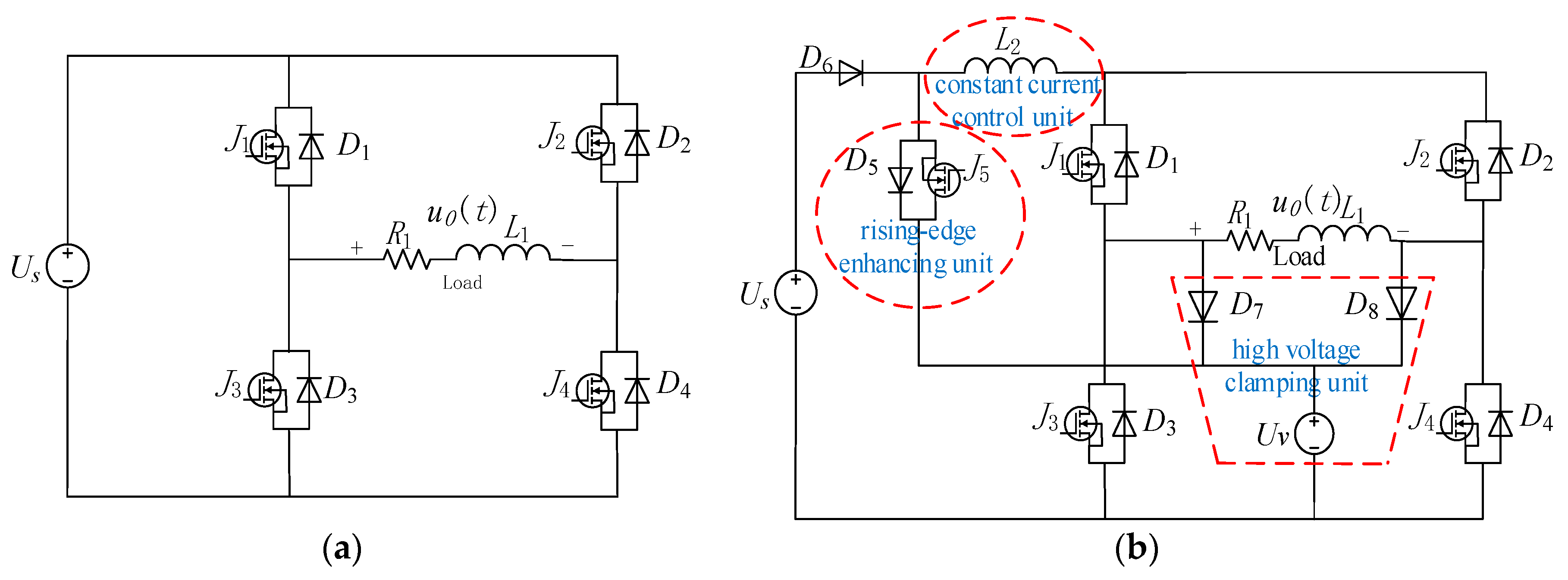
The traditional full bridge circuit model is shown in
Figure 1a, and the schematic of the proposed current source circuit is depicted in
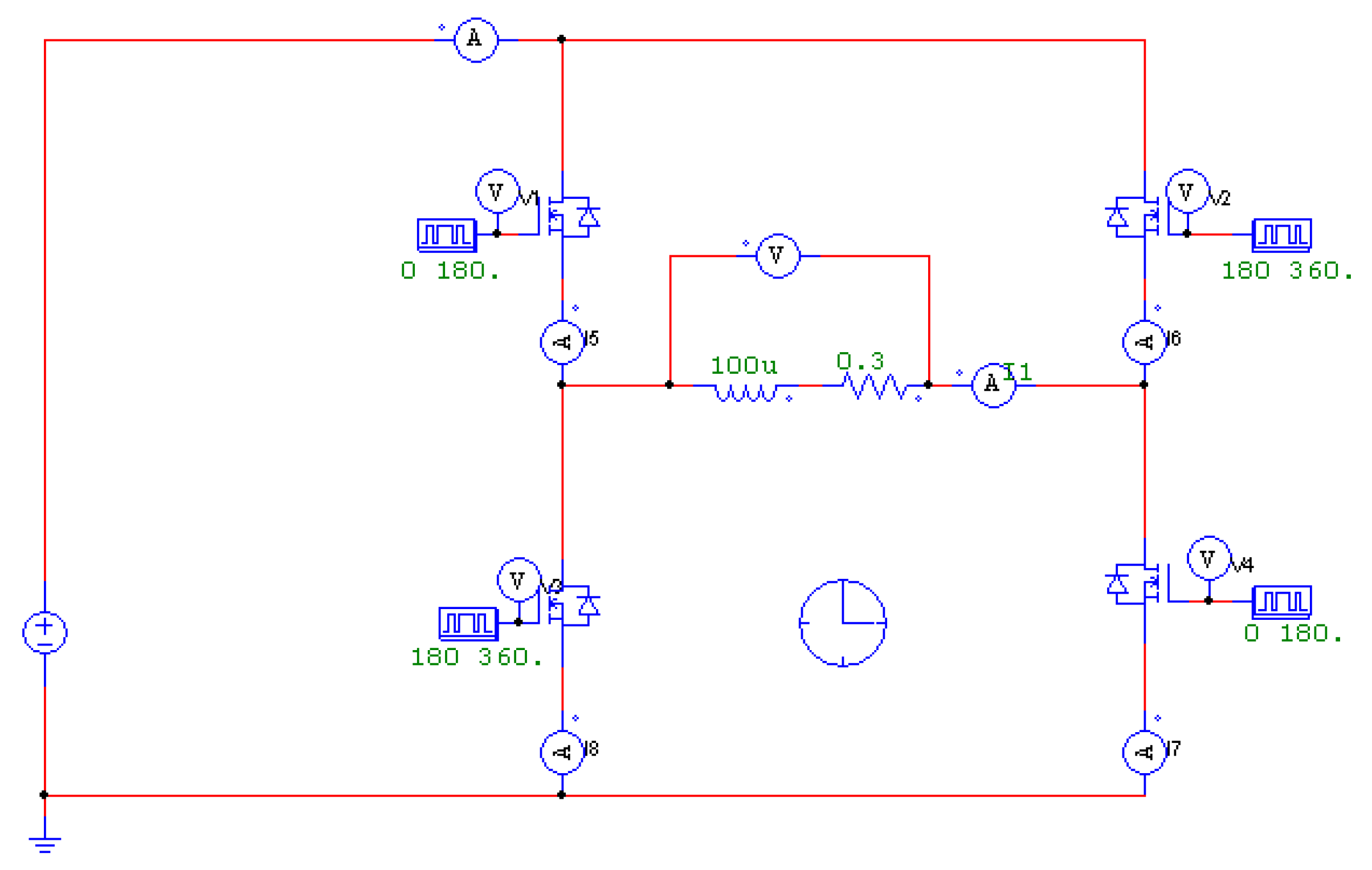
Figure 1b. The circuit consists of three major units according to its functionalities. They are rising-edge enhancing unit, constant current control unit, and high voltage clamping unit. In order to achieve linearity of the load current commutation edge, it is necessary to ensure that the load voltage is constant during current commutation. Using the existing high-speed turn-off technique, the linearity of the entire commutation edge can be achieved by clamping the load during load current rise. In this paper, in order to avoid the influence of supply voltage and output frequency on the current amplitude, the constant current source is used as the load power supply. By clamping the load voltage during the rising edge, leading edge linearity is achieved. To simplify the circuit, leading-edge boost circuit and fast turn off circuit share the same clamp circuit and clamp voltage source to achieve the consistency of rising and falling edges of the square wave current. The main circuit is shown in
Figure 1b.
The energy supplement circuit is made up of diode
D5,
J5 and clamping voltage source
Uv; the AC square wave current generator is a full bridge transmitter circuit; clamp circuit is composed of diodes
D7, D8 and clamping voltage source
Uv, Constant current inductor
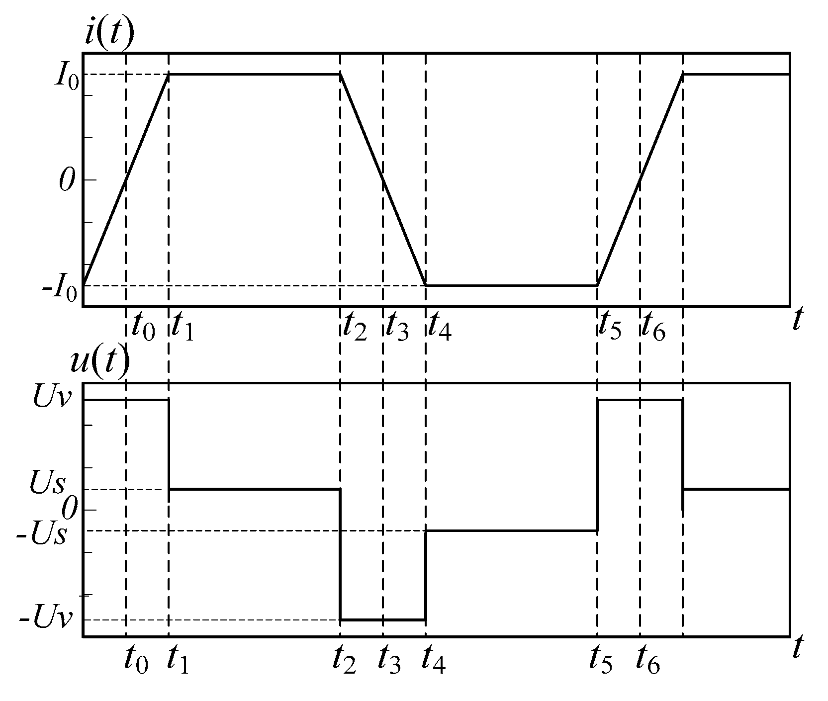
L2 is used as a constant current source. The waveforms of the load current and voltage are shown in
Figure 2.
2.2. Process of the Constant Current and Voltage Clamping Control Circuit
One charge cycle of the load current is divided into two equal time periods, that is, positive power supply time and reverse power supply time. The basic idea is that during the current commutation period, the load voltage is always been clamped to the clamp voltage source to achieve commutation direction edge linear. While during the stable positive and reverse power supply, the load inductor is powered by the constant current source in order to make sure the output current amplitude is constant. The implementation process is as follows:
In t0 ~ t1 period: switches J1 and J4 are turned on, J2 and J3 are turned off. The constant current inductor L2 and the load inductance L1 are connected in series, which have unequal initial currents. High voltage is produced at the load inductance. D7 is turned on, the current is less than the set value I0 during commutation. J5 is turned on, so the current of L2 flows through J1, D7, J5 to keep the circuit unblocked, at the same time the current of load inductor flows past R1, L1, J4, Uv, D7, the load voltage is clamped to the clamp voltage Uv, where u(t) = Uv, L1di(t)/dt = Uv, and the load current increases linearly. Uv is much larger than the DC supply voltage Us and AC square wave current linearly rises from zero to the set amplitude of load current I0.
In t1 ~ t2 period: switches J1 and J4 are turned on, J2 and J3 are turned off. The load inductance L1 and constant current inductance L2 are connected in series. When the load inductance L1 current rises to be equaled to the constant current inductance of L2, u(t) = Us, the output current is the square wave, i(t) = I0. During this period, when the load current is lower than the expected set minimum value Imin, J5 is turned on, the clamped voltage source replenishes the energy to the constant current inductance, Uv, J5, L2, J1, R1, L1, J4 form a loop, the current of constant inductor rises rapidly. When the load current exceeds the set maximum value Imax, J5 is turned off and the circuit continues to be supplied by the power supply.
In t2 ~ t3 period: switches J2 and J3 are turned on, J1 and J4 are turned off, the load current suffers a sudden change, D8 is turned on, the load current flows through R1, L1, D8, Uv, J3, u(t) changes from positive to negative, u(t) = −Uv. The voltage of the load is clamped to the clamped voltage source, L1di(t)/dt = −Uv, the square wave current begins to drop linearly, the load current i (t3) decays to zero at the time of t3, the constant current of inductor L2 flows through J2, D8, Uv, Us, D6 to charge the clamped voltage source.
For the same reason, the reverse cycle of the load current is similar to that of the positive supply cycle, which is not described here.
Analysis of the circuit shows that, the rising edge waveform of the load current of the circuit designed in this paper is linear, and when Uv >> R1I, the absolute values of the rising edge slope and the falling edge slope are equal, the waveform is symmetrical completely. The load current is constant maintained by the constant current inductance, and it has nothing to do with the supply voltage, the frequency and the load device. The main function of the diode D6 is to block the path of Uv and Us. Because of D6, when Uv is greater than Us, J5 is turned on, the clamp voltage source Uv works. Therefore, D6 is indispensable.
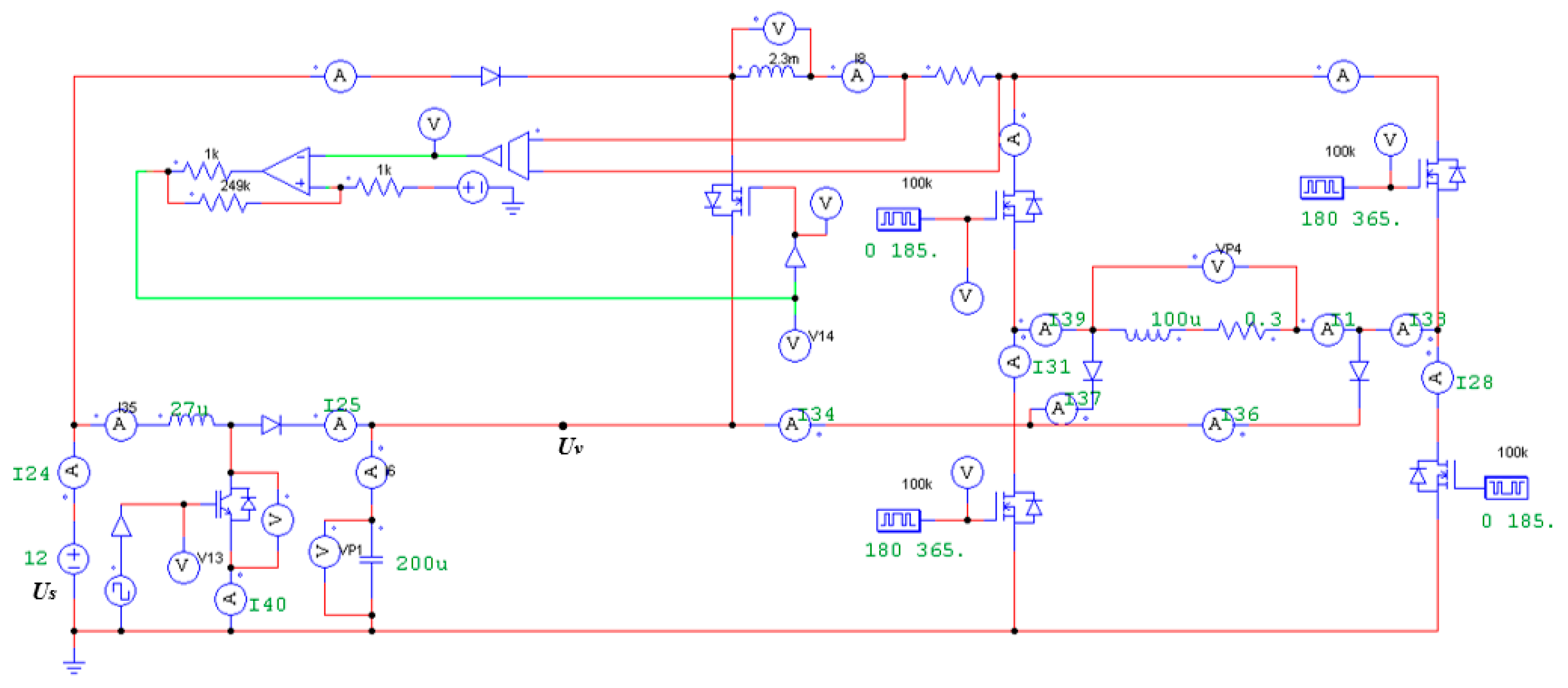
4. Simulation of Circuit Model
The wide-band banner current source circuit proposed in this paper adds constant current control and high voltage clamping measures to the traditional full-bridge circuit model. It can be realized that the amplitude of the output current is constant during the stable positive/negative power supply, and the waveform of the output current is linear during the current commutation.
In order to prove that the method can achieve the expected results, the circuit model is simulated and verified by Power Simulation software. In order to compare and analyze, this paper simulates the output waveform of the proposed circuit model and the traditional full-bridge circuit model.
Figure 3 and
Figure 4 show the schematic diagram of the traditional full-bridge circuit model and the proposed circuit model in the PSIM software simulation environment.
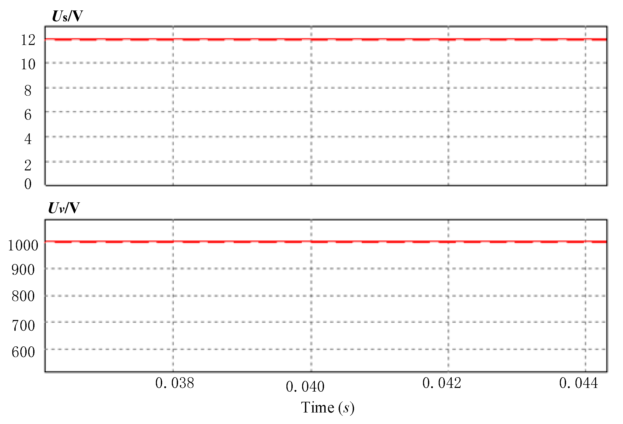
The setting parameters are as follows: supply voltage
Us is 12 V, clamp voltage
Uv is 1000 V, as shown in
Figure 5. load inductance
L1 is 100 μH,
R1 is 0.3 Ω. In the case of the same parameters, we compared the circuit proposed in this paper with the traditional full bridge circuit through simulation.
L2 is selected to tolerate a constant current below the maximum value of 15 A. At the same time, set the upper limit of current hysteresis band control as 15.5 A and the lower limit as 14.5 A. To prove that the proposed circuit is suitable for a very wide frequency band, five frequency points are selected between 500 Hz and 100 KHz for simulation, which are 500 Hz, 1 KHz, 10 KHz, 50 KHz, 100 KHz. The comparisons of the simulation load responses between the full-bridge circuit and the proposed circuit are shown in
Figure 6,
Figure 7,
Figure 8,
Figure 9 and
Figure 10.
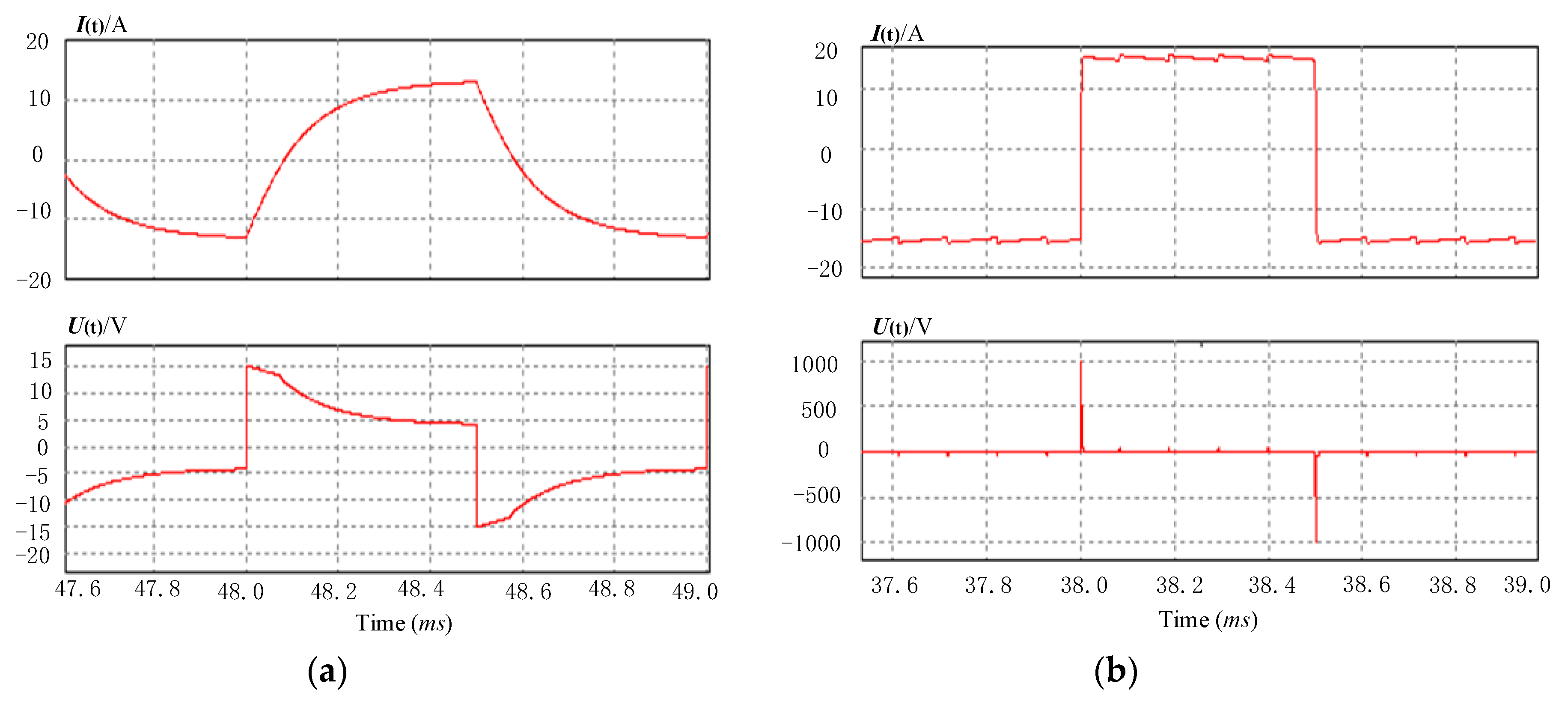
It can be seen from
Figure 6 and
Figure 7 that at the lower frequencies of 500 Hz and 1 KHz, the current waveform of the output of the traditional full bridge circuit is irregular, and the amplitudes are 15 A and 12 A. The output current waveform of the circuit presented in this paper is basically stable at 15 A in the flat region.
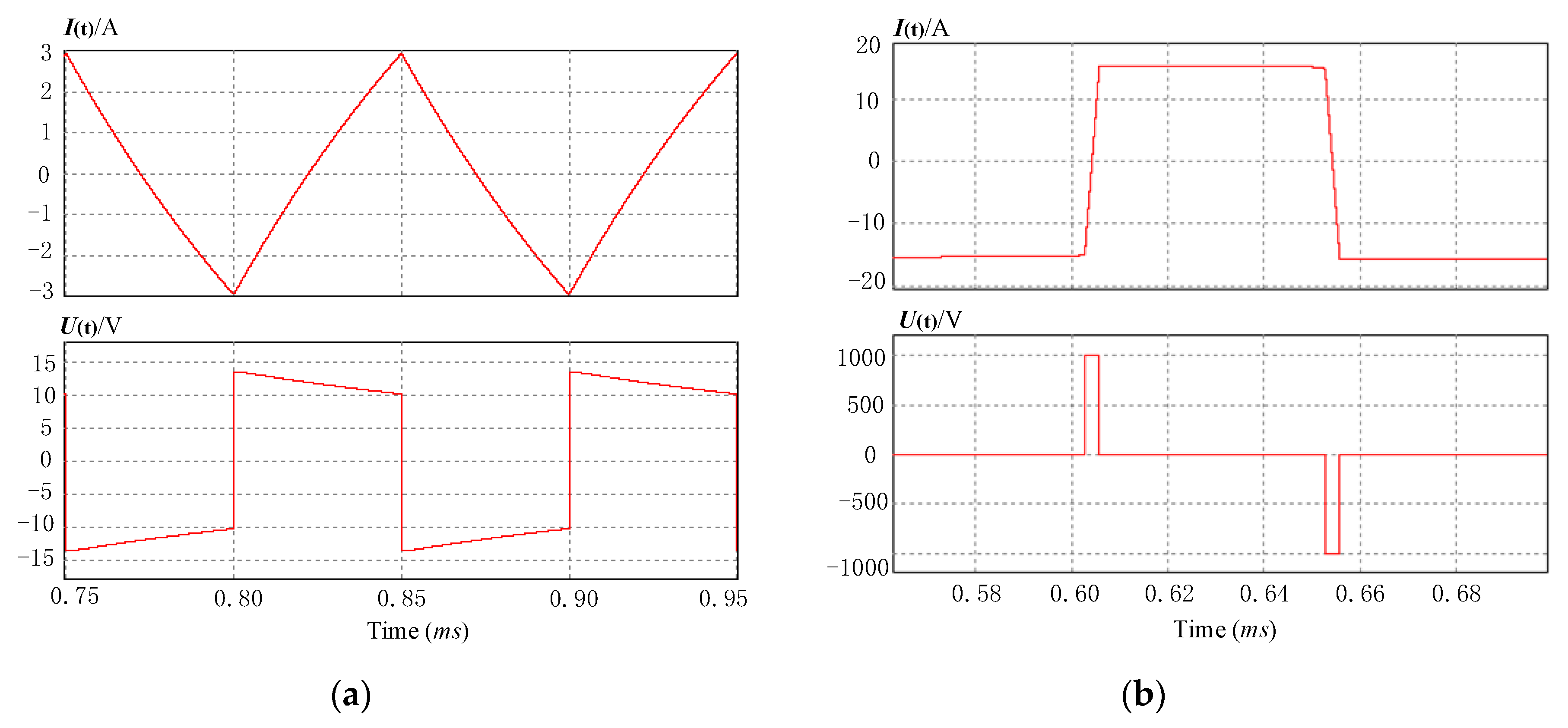
Figure 8 shows that when the frequency is 10 KHz, the output waveform of the traditional full-bridge circuit is similar to that of the triangular wave, and the amplitude is 3 A. The circuit output current waveform proposed in this paper is linear during the rising/falling period, the flat region is stable, no fluctuation, and the amplitude is stable at 15 A.
Figure 9 and
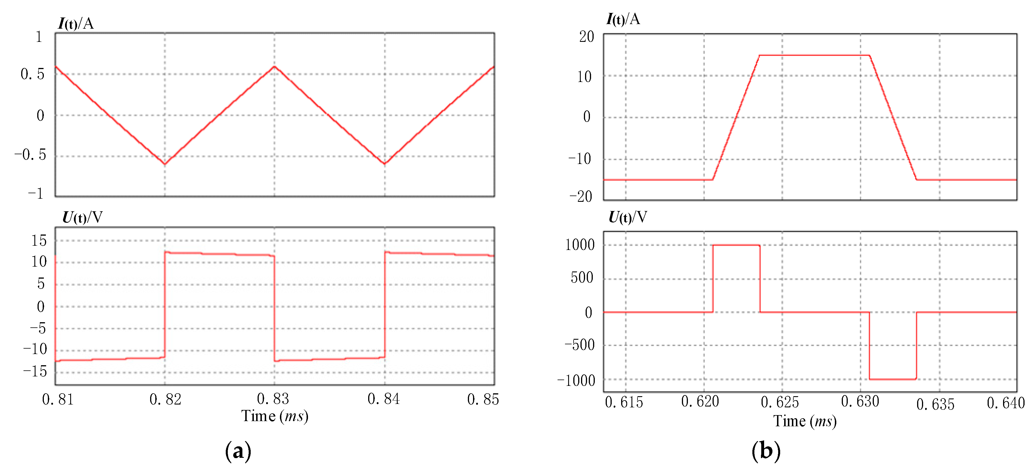
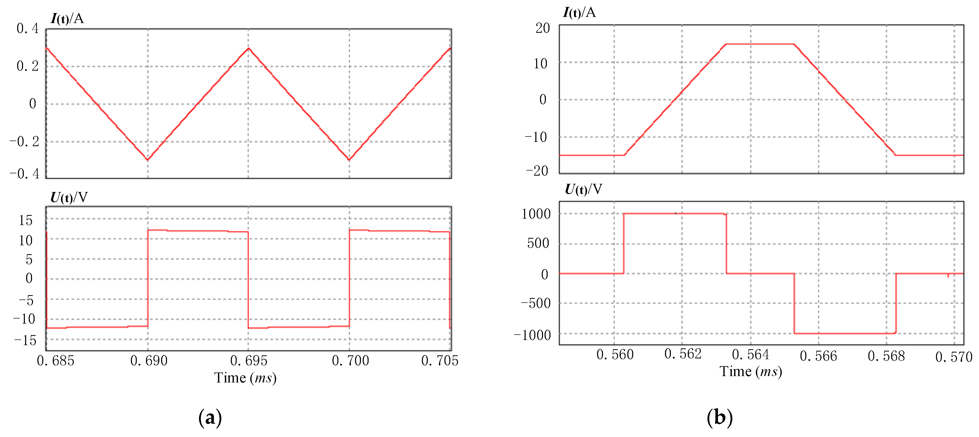
Figure 10 show that at the higher frequency of 50 KHz and 100 KHz, the current waveform of the output of the traditional full bridge circuit is triangular wave with amplitudes of 0.6 A and 0.3 A respectively. The current waveform of the circuit output proposed in this paper is stable in the flat region, and the amplitude is stable at 15 A. The linearity is high during the rising/falling period.
As shown in
Figure 6,
Figure 7,
Figure 8,
Figure 9 and
Figure 10, as the frequency increases, the output current amplitude of the traditional full-bridge circuit gradually decreases, and the waveform gradually changes from irregular to triangular wave; the output voltage amplitude is equal to the supply voltage Us of 12 V, and the waveform changes from irregular to square wave, but at the flat region always unstable.
In the case of the same circuit parameters, since the circuit proposed in this paper adds constant current control and voltage clamping measures, the output current waveform does not fluctuate with changes in frequency, source voltage and load. While the clamp voltage is 1000 V DC voltage, the current of the circuit I rises to the set value with fast rising edge at a rate of 107 A/s and maintains at 15 A when the current is in steady state. This means that this kind of circuit can well operate in a wide frequency range and simultaneously maintain constant output current, from 500 Hz to 100 kHz.
According to di(t)/dt = −Uv/L1, in the case of the inductance, the circuit was defined and the rise steepness of the current was proportional to the value of the clamp voltage Uv. The higher the clamping voltage, the faster the rate of change of the rising edge of the current, the shorter the time it takes for the current to rise, and thus the cycle decreases and the operating frequency of the circuit increases. On the contrary, the lower the clamp voltage, the slower the rate of change in the rising edge of the current, the longer the current rise process, and the longer the cycle, the lower the operating frequency of the circuit. E.g., if the clamp voltage Uv is changed from 1000 V to 500 V, the slope of the current change will be half of the original, it is needed much more time to reach the specified current I0, the cycle becomes larger, the operating frequency is reduced. In the case of equipment conditions permitting, the higher clamp voltage Uv, the better. Of course, in reality, the voltage cannot be increased indefinitely due to the limitation of the performance of the circuit device.
5. Experimental Results
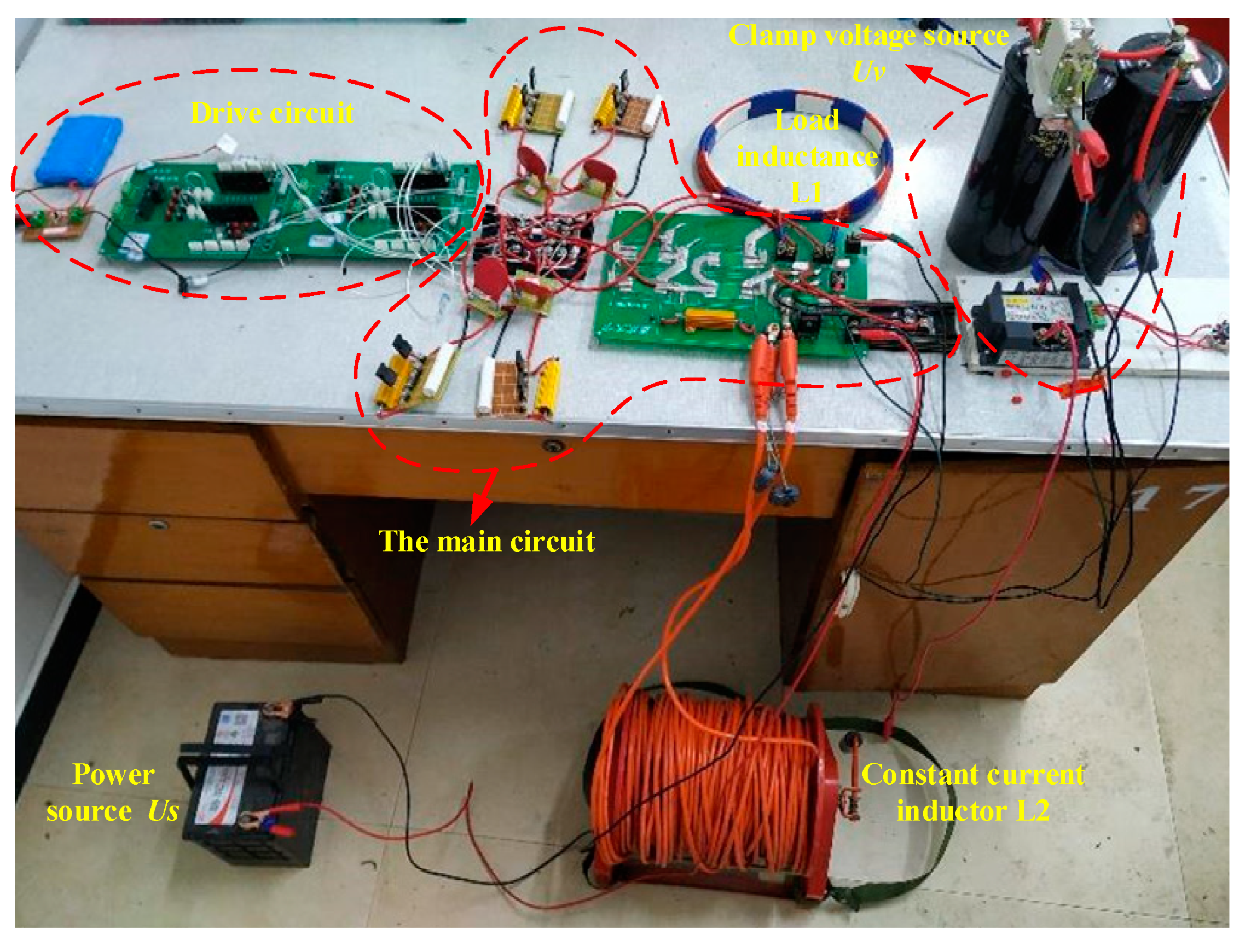
In order to experimentally verify the constant current and voltage clamping control circuit proposed in this paper, the experimental circuit is established according to
Figure 1b. The main circuit of the experiment is shown in
Figure 11. The supply voltage
Us is 12 V, clamp voltage
Uv is 1000 V, load inductance
L1 is 100 μH, constant current inductor
L2 is 2 mH. The maximum current in the circuit is about 15 A, and the voltage stress of the switching device is about 1000 V. Considering a certain voltage and current margin, Mosfet (C2M0045170D) and Dioxide (DSDI60-16A) are selected according to the datasheet. The main device parameters of the circuit are shown in
Table 1.
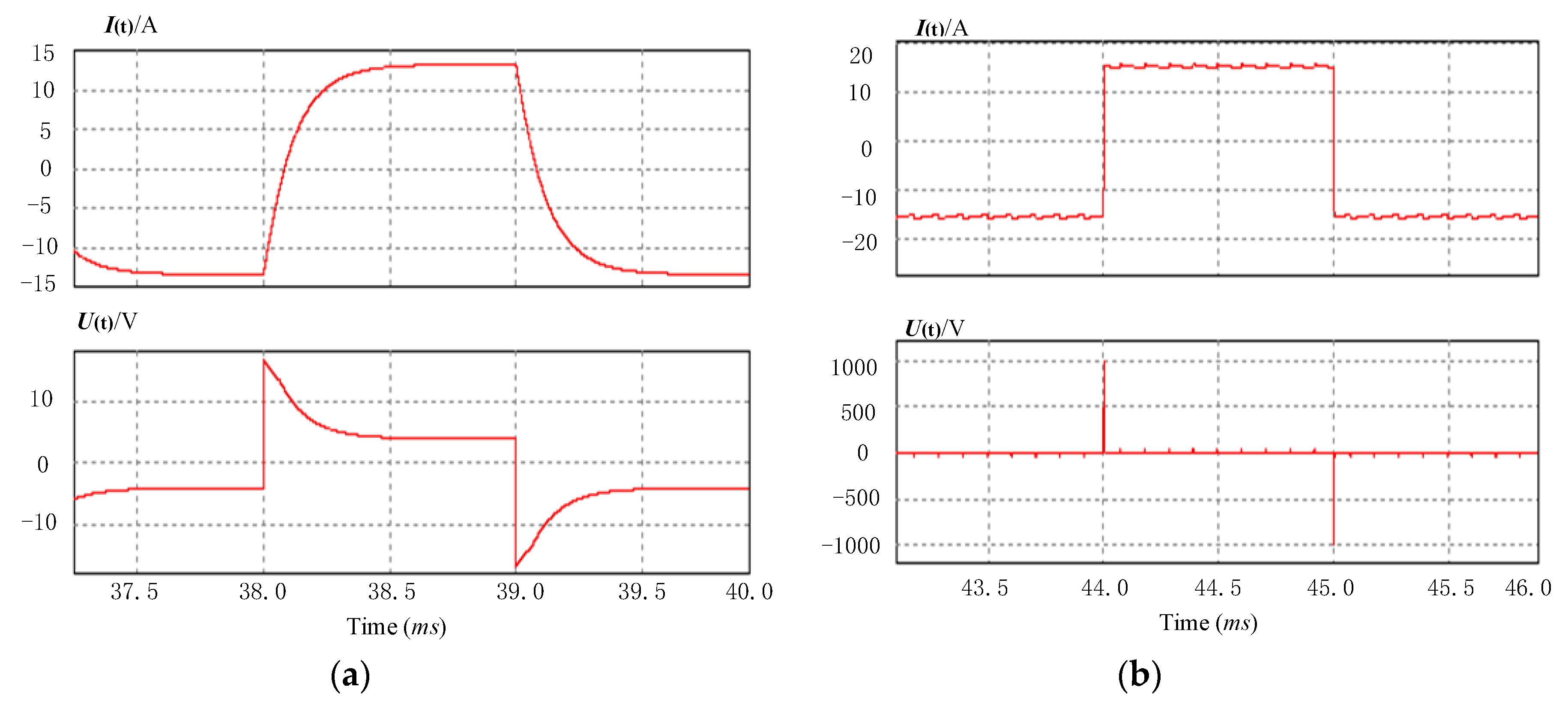
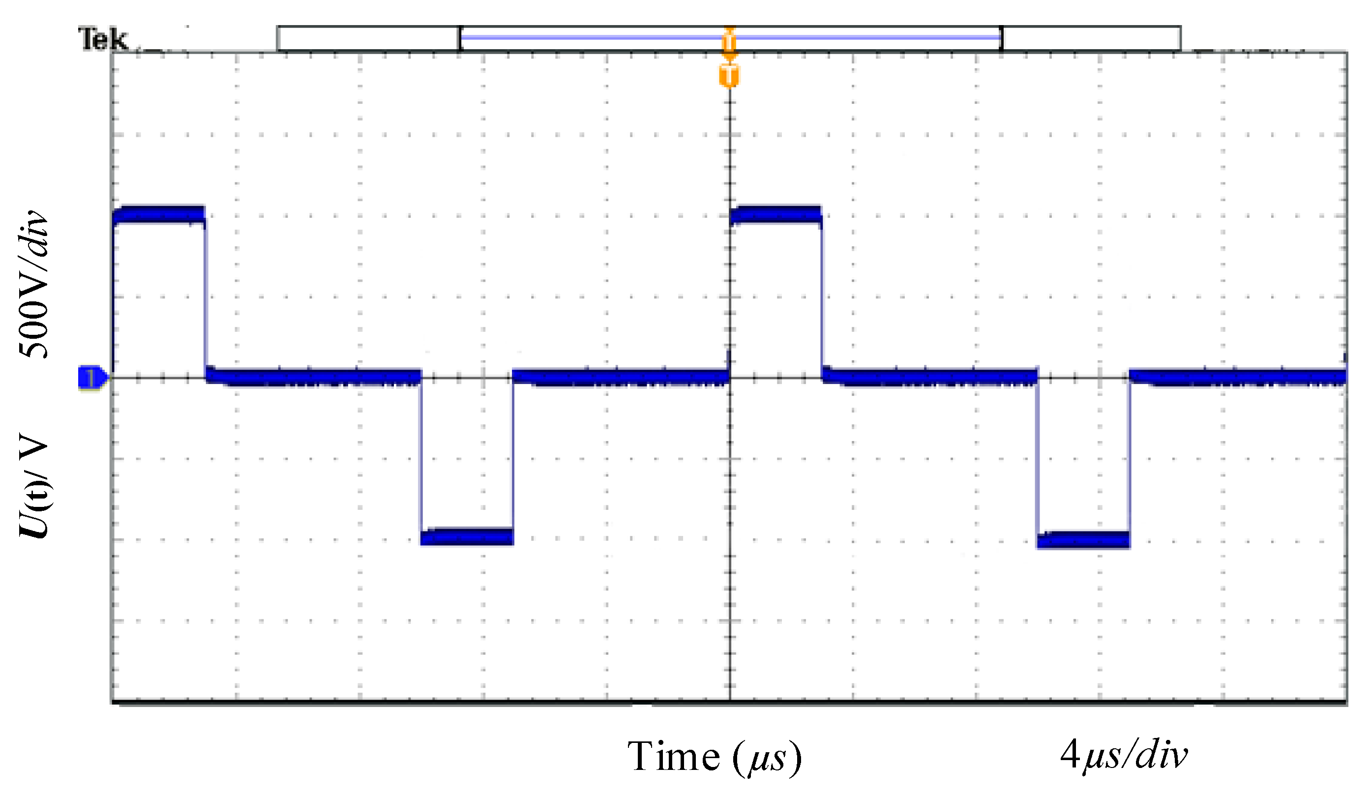
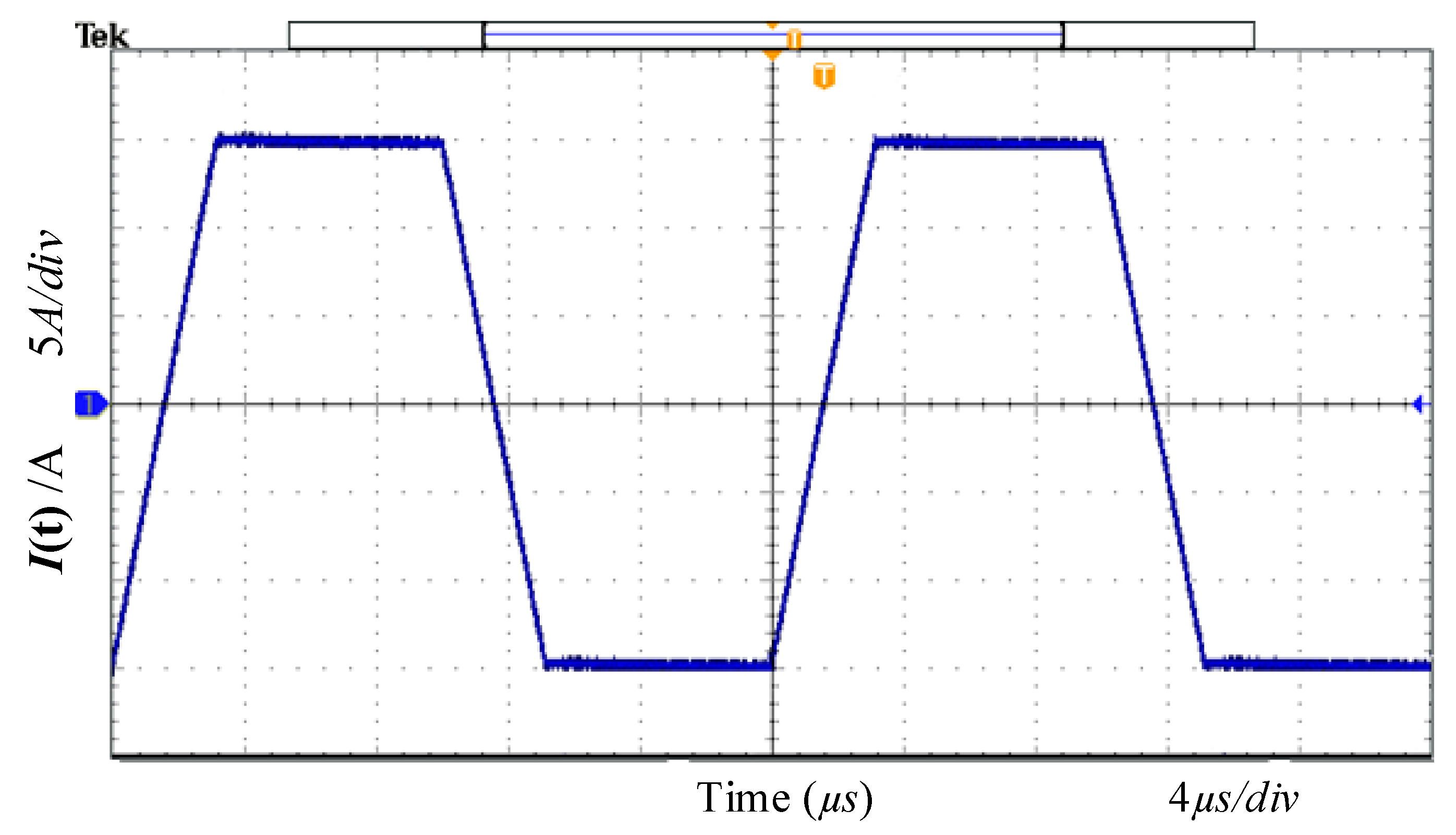
Limited by the performance of existing electronic devices, our experimental circuit can output stable waveforms of voltage and current with the maximum frequency of 50 KHz. The experimental results waveform of the voltage and current are shown in
Figure 12 and
Figure 13 respectively. It is shown in
Figure 12, during the experiments, that the load voltage is always been clamped between 998 V and 1002 V, and the waveform quality is very stable.
Figure 13 shows that during the experiments the maximum output current of the circuit can reach up to 15 A, the current variation range in the flat phase is only 0.2 A.
Figure 13 also shows that the output current waveform of the circuit maintains with high linearity during commutation, the commutation delay is less than 3 μs and the slope of the commutation edge is linearly stable. The experimental results shown in
Figure 12 and
Figure 13 indicate that the constant current and voltage clamping control circuit proposed in this paper has reached the intended purpose of fast rising edge and amplitude constant.
The experimental results show that the circuit proposed in this paper provides energy for the load by the constant current source. During the current commutation, the load voltage is clamped in a constant voltage, and the linearity of the commutation of the square wave current is realized. At the same time, in order to simplify the circuit, the leading-edge boost circuit and fast shutdown circuit share the same clamp circuit and clamp voltage source, while achieve the consistency of rising/falling edge of the square wave current. In the case of constant current control, the paper achieves that the output current does not change with the change of the power supply voltage, the frequency and the load device. The current rise (down) is fast, there is no dead zone in the middle section, the duty ratio is high, and the amplitude is constant in the flat phase. Controlling the clamped voltage source can control the steepness of the positive and negative edge, increase the clamp voltage, reduce commutation delay and improve the switching frequency.
6. Conclusions
In this paper, a bipolar broadband AC pulse current source emission circuit has been developed for the key technical problems such as rapid commutation of transmission current, constant linearity, wide frequency transmission and constant current amplitude in the existing frequency domain electromagnetic transmitter. The leading-edge linear technique and the constant-current control strategy of load current are proposed to realize wide-band constant-amplitude AC square-wave current emission of inductive load. By applying a constant high voltage clamp to the load during the current commutation to achieve the commutation edge linearity. Controlling the clamped voltage source can control the steepness of the positive and negative edge, increase the clamping voltage, reduce commutation delay and improve the switching frequency. In the case of constant current control, the paper achieves that the output current does not change with the changes of the power supply voltage, the frequency and the load device. The maximum transmission frequency is 100 KHz, the maximum emission current is 15 A; the current can rise quickly to the set value with very large slope of 107 A/s. The current can be quickly turned off from the amplitude of the positive polarity to the amplitude of the negative polarity. Without a dead zone in the middle section, the amplitude is constant in the flat stage; the amplitude of the current in the high frequency range is increased from 3 A to 15 A.


