Article

Channel Length Biasing for Improving Read Margin of the 8T SRAM at Near Threshold Operation

1
Department of Electronic Engineering, Kyung Hee University, Yongin 17104, Korea
2
School of Electrical and Computer Engineering, UNIST, 50 UNIST-gil, Ulsan 44919, Korea
3
School of Electronic and Electrical Engineering, Hongik University, Seoul 04066, Korea
*
Author to whom correspondence should be addressed.
Electronics 2019, 8(6), 611; https://doi.org/10.3390/electronics8060611
Submission received: 30 April 2019 / Revised: 24 May 2019 / Accepted: 27 May 2019 / Published: 30 May 2019
(This article belongs to the Special Issue Low-Voltage Integrated Circuits Design and Application)

Abstract

:
Reducing a supply voltage in order to minimize power consumption in memory is a major design consideration in this field of study. In static random access memory (SRAM), optimum energy can be achieved by reducing the voltage near the threshold voltage level for near threshold voltage computing (NTC). However, lowering the operational voltage drastically degrades the stability of SRAM. Thus, in conventional 6T SRAM, it is almost impossible to read exact data, even when a small process variation occurs. To address this problem, an 8T SRAM structure is proposed which can be widely used for improving the read stability at lower voltage operation. In this paper, we investigate the channel length biasing effect on the read access transistor of the 8T SRAM in NTC and compare this with 6T SRAM. Read stability can be improved by suppressing the leakage current due to the longer channel length. Simulation results show that, in NTC, up to a 12× read-error reduction can be achieved by the 20 nm channel length biasing in the 8T SRAM compared to 6T SRAM.

1. Introduction

As the demand for mobile and wearable applications continues to increase, the importance of dynamic power as well as standby leakage power consumption with limited battery size has been increasing [1,2,3]. Logics or processors usually operate at a slower frequency for minimizing dynamic power. The memory module, such as static random access memory (SRAM), is the largest component which consumes significant leakage power in low-power integrated circuits (ICs) such as these [4]. Recently, near threshold voltage computing (NTC) has become popular as a demand for extremely low-power applications increases [5,6,7]. Decreasing the supply voltage near or under the threshold voltage level minimizes the dynamic power of the circuits due to the quadratic dependency of VDD to power [2,3,8]. However, the reduced voltage level leads to a very large performance degradation and an exponential increase in the variations [2]. Thus, a conventional 6T SRAM is not suitable for NTC applications due to the reduced noise margin and reduced bit-line sensing margin. Decoupled SRAM cells, such as the 8T and 10T architectures, by isolating memory cells from the bit line, have been introduced and adopted for robust operation in low voltage environments [4,9,10,11,12,13,14,15]. In those designs, the read bit line is decoupled with the cell storage so that other transistors do not affect the read operations. Correct sensing of the read bit line of the 8T SRAM at lower power supplies (i.e., near- or sub-threshold voltage) is another challenging issue because cell leakage currents in the other bits (inactive) connected at the same bit line are significant at low voltage operation. The leakage currents due to the inactive bits can reduce the noise margin of the active cell when being read.
Several circuit-level assist techniques are proposed to improve the V m i n (the minimum operating voltage) and the SRAM stability [16,17,18,19,20,21]. For readability assist, negative GND, VDD boosting, and word-line boosting methods can be used. However, these solutions complicate the design and layout, and thus increase area and power consumption by additional circuitry.
In this study, we exploit a channel length biasing technique in the access transistor of the read line of the 8T SRAM to reduce cell leakage when inactive and improve the reliability of the read operation at lower supply voltage (e.g., 0.4 V for near threshold voltage (NTV) operation). Both 6T SRAM and 8T SRAM layouts are drawn in the commercial 65 nm process. The extracted layouts are analyzed and compared in the read operation for the leakage currents and reliability characteristics.

2. Operation and Design of 6T and 8T SRAM

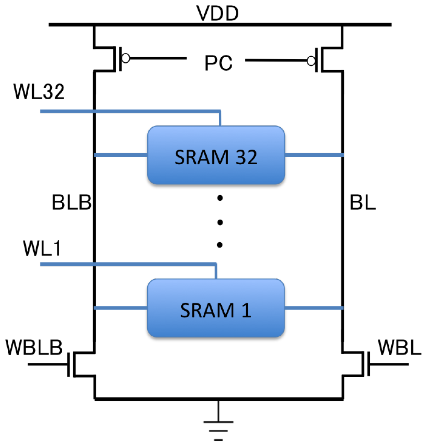
The conventional design of the 6T and 8T SRAMs’ one bit cell are shown in Figure 1. The SRAM consists of cross coupled inverters for data storage, access transistors (M1 and M2) to read and write data, and differential bit lines (bit line (BL) and bit line bar (BLB)). As shown in Figure 1b, two more transistors (M3 and M4) are added for additional read word line (RWL) and read bit line (RBL) in the 8T SRAM. The Q contains the logic data and QB holds the complementary value statically, provided the proper power supply is applied to the inverters. In the array type memory, the word line (WL) accesses multiple pieces of data in a row simultaneously and multiple cells (e.g., 32-bit cells) share the BL (and BLB) together in a column, as shown in Figure 2. During read operation, both the BL and BLB are charged to pre-defined voltage values (e.g., VDD or VDD/2) and the WL for a specific memory cell is increased to initiate the reading operation. Then BL and BLB begin to either discharge or maintain the precharged values, depending on the logic value they contain. For example, assuming logic ‘1’ is stored in the Q (QB = ‘0’), the BLB discharges, and BL remains in its precharged value and vise versa. A sense amplifier circuitry is added to detect the small current changes in the BLB and BL and to amplify them for fast and reliable reading.
The traditional 6T SRAM is very simple and robust in design. It has been used successfully in various applications for many years [22]. However, because of the read and write failures caused by the reduced noise margin and sensing margin, the traditional 6T SRAM architecture is not suitable for use at low voltage. The failures are attributed to the ever-increasing leakage current and process variations at the lower supply voltage (e.g., NTC) as technology scaling continues. For example, in read operation, the BL should maintain the precharged value when Q is holding logic ‘1’ (QB = ‘0’), but the BL will drop because of the leakage current through M2 transistors in the other cells in the same column (i.e., inactive or WL is low). The worst leakage current can flow when all other cells are storing ‘0’ (Q = all ‘0’ and QB = all ‘1’). If the reduced BL reaches lower than a certain sensing margin, an incorrect data value can be detected and read at the end.
On the other hand, in the 8T [12], the WL signal is used for the writing operation and the RWL is used for the reading operation. When the read operation starts, the RBL is charged, and the RWL is then increased to access the data stored in the cross-coupled inverters. The RBL must not change when QB is ‘0’ (Q = ‘1’) and will discharge when QB is storing ‘1’ (Q = ‘0’). As shown in the Figure 1b, the read line is connected to the QB signal; therefore, the bit patterns of the worst leakage for the read operation are Q = all ‘0’ (or QB = all ‘1’) except Q = ‘1’ (or QB = ‘0’) at the cell to read (e.g., 32th bit). In this condition, the pull-down transistors of the read line (M3) at the inactive cells are all ‘on’ states and the drain of the M3 is discharged to zero. Thus, significant leakage current is drawn through the access transistors (M4) from the bit line (RBL), lowering the voltage level which should be maintained at ‘high’ for correct operation in reading ‘1’. We increase the channel length of the read access transistor (M4) in the red circle shown in Figure 1b to exploit the leakage current reduction with a longer channel length. The reduced leakage current increases the bit sensing margin between ‘0’ and ‘1’, which is crucial in NTV operation. The data patterns for the best leakage current and the worst leakage current are summarized in Table 1.
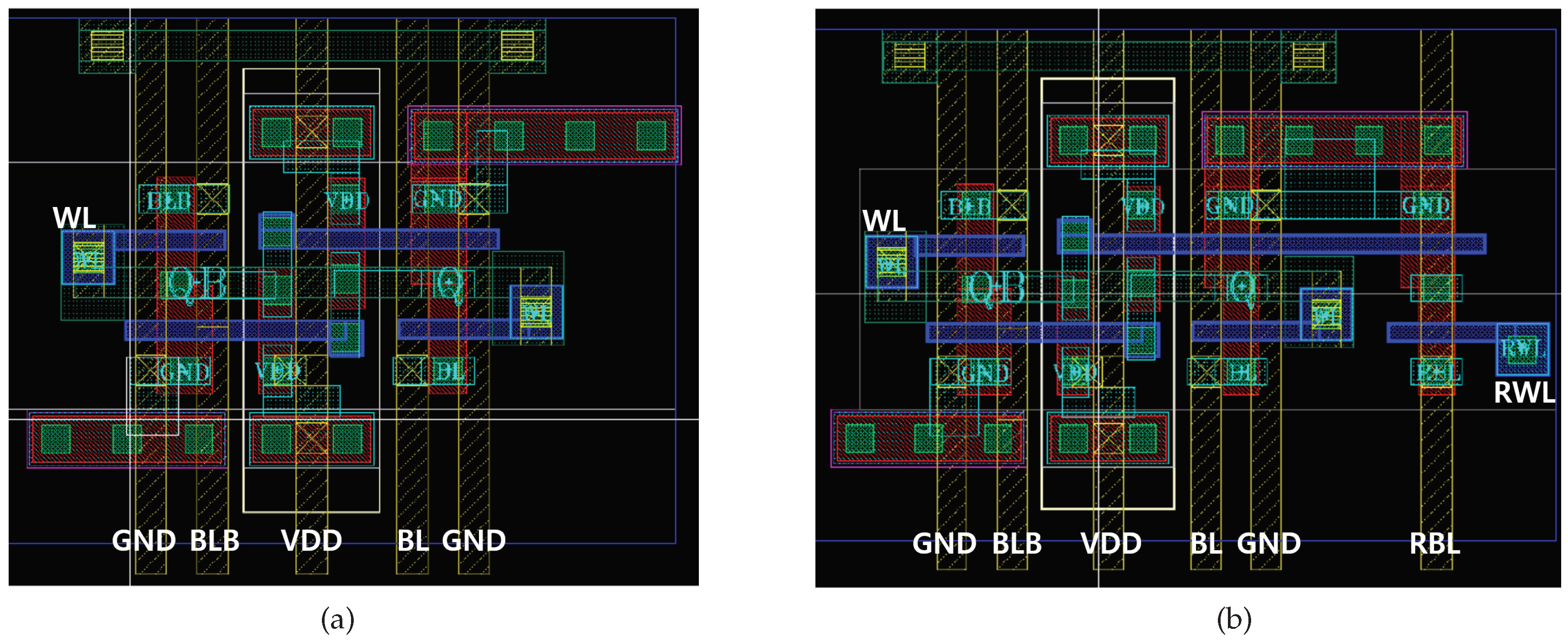
The transistor sizing for one bit cell of 6T and 8T SRAM, which are presented in Figure 1 and Figure 3, is summarized in Table 2. The minimum channel length and width are used for the PMOS pull-up transistors and two access transistors. In addition, the size of the NMOS pull-down transistors of the cross-coupled inverters was increased to prevent the read upset problem.
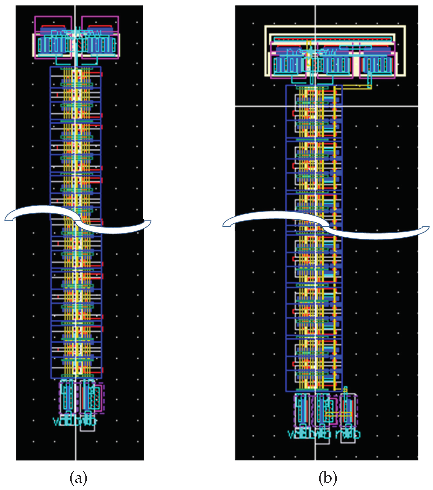
In this study, we design one column of 32-bit memory cells for simulation, as shown in Figure 4. As mentioned in the previous sections, all memory cells share the vertical metal of the BL, BLB, and RBL. Thus, even in inactive mode (or when WLs are low), the leakage current through the access transistors can reduce the voltage level during the read operation.
As shown in Figure 3a, the SRAM core has five parallel vertical metal lines (yellow): GND, BLB, VDD, BL, and GND from the left. The two reasons for the order of these parallel metal lines are as follows. First, if the signal lines (BLB or BL) are located close to another signal line, coupling between signals can occur, causing a crosstalk effect [23]. Second, the order is related to the so-called Miller effect [24], whereby the effective capacitance between two metal plates increased two-fold when the potential of each conductor changes in the opposite direction. For example, the effective capacitance between BLB and BL becomes large if they are positioned close to each other and the increased capacitance (effective) slows down the SRAM performance. Therefore, the signal lines are located between the GND and VDD lines for shielding. The minimum spacing between metal lines and metal width is 100 nm which is the minimum value. The 8T SRAM illustrated in Figure 3b shows two additional transistors at the right side of the 6T SRAM core. For channel length biasing analysis of the 8T SRAM, five layouts with different channel lengths (60–100 nm with 10 nm steps) at the M4 read access transistor are drawn and the layout RC parasitics are extracted and annotated to ensure simulations are more accurate.

3. Channel Length Biasing for Leakage Reduction

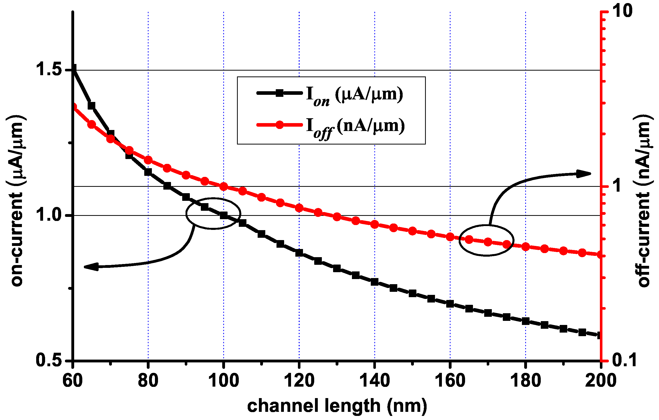
The channel length (L) is one of the major parameters for the performance (I o n ) and standby leakage current (I o f f ) of the transistors [25,26]. The impact of the on- and off-state current (I o n and I o f f , respectively) for different channel lengths of the NMOS at 0.4 V supply voltage is shown in Figure 5. As shown in the figure, I o n reduces by 30%, but I o f f reduces by 3× as the channel length increases from 60 to 100 nm in the commercial 65 nm technology node in the worst leakage condition (i.e., fast process corner (FF) and high temperature (120 °C)).
Threshold voltage, V t h , which has the greatest influence on I o n and I o f f , depends on the channel length (L). V t h roll-off phenomenon, in which V t h decreases as the channel length is reduced, occurs because of the presence of 2D field patterns in short channel devices instead of 1D field patterns in long-channel devices [25]. The proximity of source and drain regions enhances the 2D field pattern. In the longer channel devices, their depletion regions have little effect on the potential profile or field pattern in most parts of the channel, since the source and drain are far apart. Thus, leakage current (I o f f ), which has an exponential dependency on V t h , is reduced as the channel length increases, as shown in Figure 5.

Trip Voltage

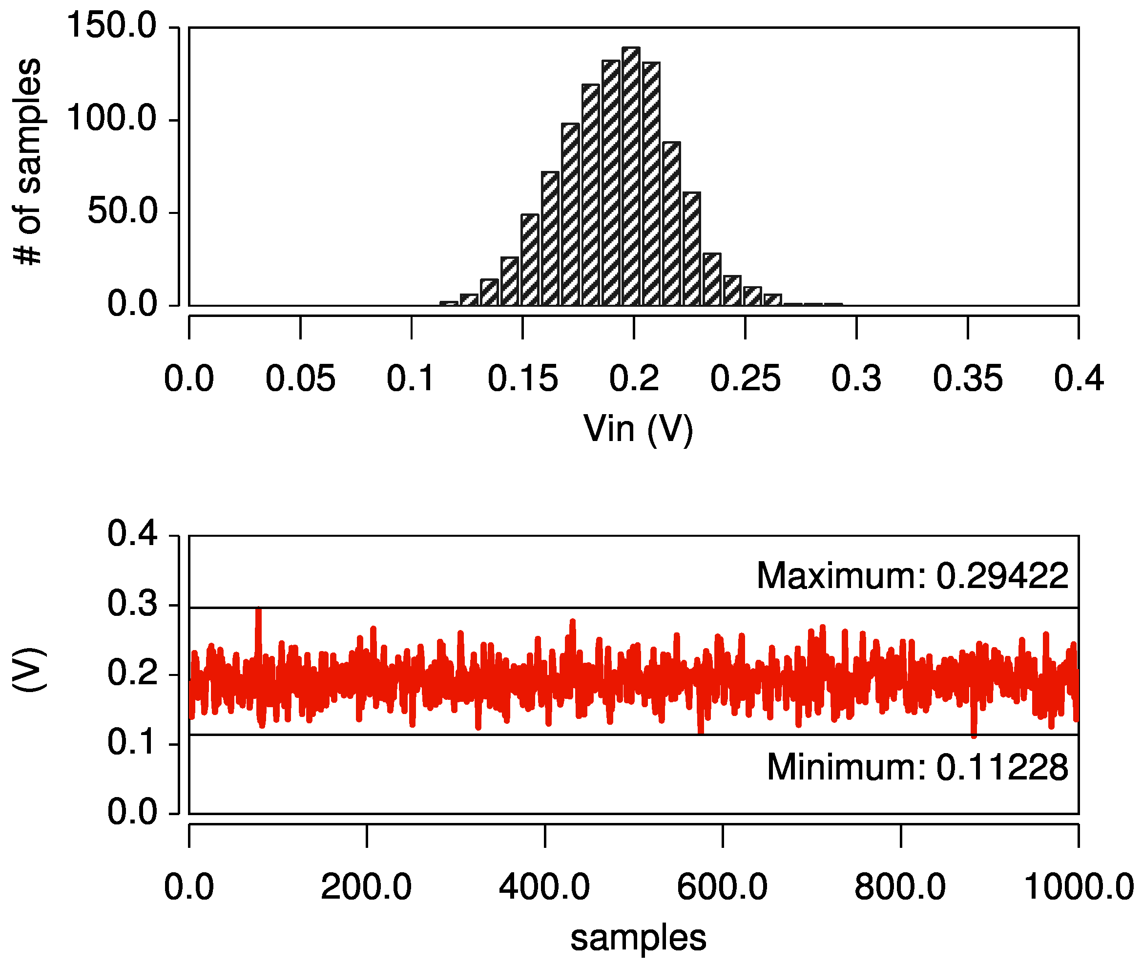
The trip voltage of an inverter is used to define the read margin of an SRAM cell, and it is the maximum and minimum bit-line voltage to sense (read) the ‘0’ and ‘1’ value correctly [16]. For the statistical trip voltage and sensing margin analysis of the design, 1000 Monte Carlo (MC) simulations were conducted as shown in Figure 6. As can be seen, a MC statistical analysis of the cross-coupled inverters indicates that the V I H (the minimum input ‘high’ value of an inverter for output of a logic ‘0’) is 0.29 V and V I L (the maximum input ‘low’ voltage of an inverter for output of a logic ‘1’) is 0.11 V at 0.4 V VDD operation. The results thus imply that any voltage levels between V I H and V I L will not be sensed correctly in the SRAM read. Therefore, a high precharged value at the BL should not drop below 0.29 V due to the leakage currents of the inactive cells for correct ‘1’ read, and the pull-down transistor must reduce the bit line to below 0.11 V for correct ‘0’ read operation before sensing starts.

4. Simulation Result

In the simulations, 0.4 V nominal voltage was used for VDD. Simulations were conducted with extracted netlists from the drawn layouts. All proper control signals were set for read operation and the worst leakage condition (FF process corners at a temperature of 120 °C) was used in the analysis.
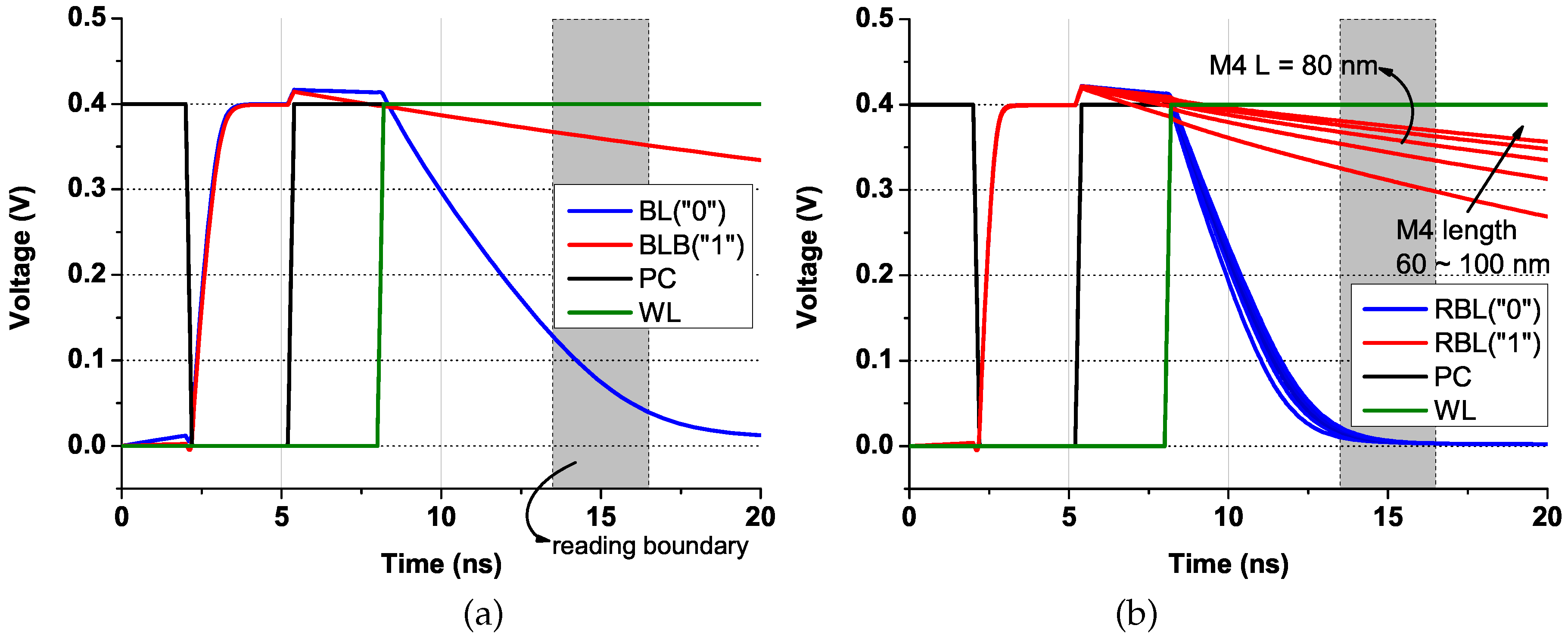
The reference time required for sensing the bit line varies according to the process variation of the transistors. An MC-based statistical analysis of 60-stage inverter chain shows that timing variation can reach up to ±10% from the reference time. Therefore, we set 15 ns as the nominal sensing reference time, 13.5 ns as the earliest sensing time, and 16.5 ns as the latest sensing time. For the correct bit-line sensing, the bit-line margin value should be larger than the trip point voltage, which was obtained from the above analysis, during the entire timing variation interval in sensing (i.e., between 13.5 ns and 16.5 ns).
Figure 7 shows the simulation results of 6T and 8T SRAM in the reading operation with the worst leakage bit-cell conditions, as described in Table 1. As can be seen from the figures, the BLB in 6T and the RBL voltage in 8T SRAM dropped gradually due to the leakage current caused by the inactive cells. The decrement of the RBL voltage in the 8T SRAM reduces as the channel length increases, as a result of the leakage current reduction.
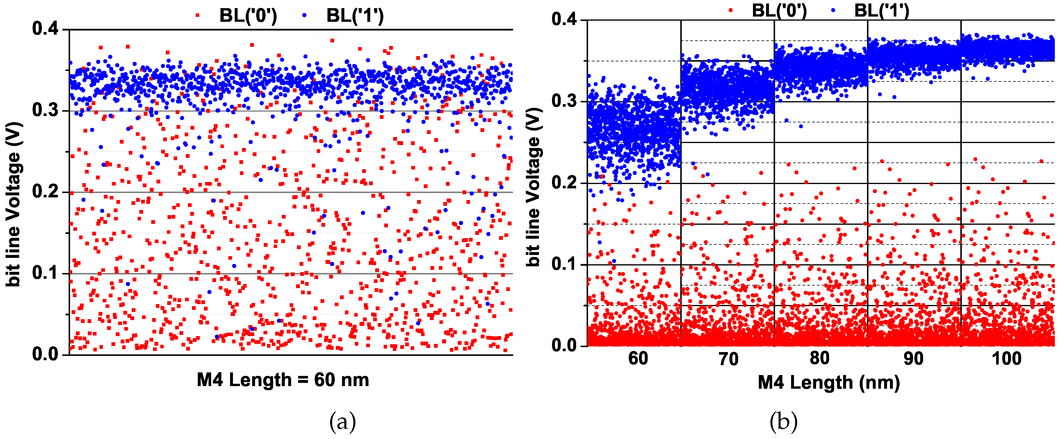
The Monte Carlo simulations of 1000 samples in 6T and 8T of five different channel lengths (e.g., L = 60–100 nm) are shown in Figure 8a,b, respectively. As shown, the reading ‘0’ (red) fails (i.e., above 0.11 V) in most samples in the 6T SRAM at low voltage operation. While the reading ‘0’ improves significantly in the 8T SRAM, the many samples of the ‘1’ read (blue) fails (i.e., below 0.29 V) as a result of the huge leakage current for the minimum channel length (L60 nm) at VDD0.4 V. However, the number of errors reduce significantly with L = 80 nm and an error in reading ‘1’ does not occur with longer channel lengths (L90 nm or 100 nm) because of the reduced leakage current (i.e., the bit-line voltages are larger than V I H ∼ 0.29 V).
The error-rates comparison between 6T and 8T is summarized in the Table 3. As shown, the 6T structure is not recommended in NTC due to the many reading errors both for ‘0’ and ‘1’. While the reading ‘0’ improves significantly with the 8T design, the high error probability in reading ‘1’ according to the minimum channel length of the M4 transistor should be avoided. In addition, when the channel length of M4 becomes larger than 80 nm, the error probability in reading ‘1’ reduces to almost zero.

5. Conclusions

In this study, we analyzed the 6T and 8T SRAM cells at near-threshold voltage operation. The channel length biasing technique is proposed in the 8T SRAM for reducing leakage current of the inactive cells and increasing the sensing margin at low voltage. Layouts are drawn in 65 nm technology and simulations are conducted at the worst leakage conditions. Monte Carlo simulations show that a channel length of 20 nm longer than the minimum at the read access transistors of the 8T SRAM is good trade-off in reducing significant leakage current, thus increasing the noise margin at NTC (e.g., VDD = 0.4 V).

Author Contributions

Conceptualization, I.J.C. and Y.K. (Youngmin Kim); methodology, I.J.C. and Y.K. (Youngmin Kim); software, Y.K. (Yesung Kang); validation, Y.K. (Yesung Kang); investigation, I.J.C., Y.K. (Yesung Kang), and Y.K. (Youngmin Kim); resources, Y.K. (Yesung Kang) and Y.K. (Youngmin Kim); writing—original draft preparation, Y.K. (Yesung Kang); writing—review and editing, I.J.C. and Y.K. (Youngmin Kim); supervision, Y.K. (Youngmin Kim); project administration, Y.K. (Youngmin Kim); funding acquisition, Y.K. (Youngmin Kim).

Funding

This research was funded by the Ministry of Education grant number NRF-2017R1D1A1B03028065.

Acknowledgments

This research was supported by the Basic Science Research Program, through the National Research Foundation of Korea (NRF), funded by the Ministry of Education (NRF-2017R1D1A1B03028065).

Conflicts of Interest

The authors declare no conflict of interest.

References

  1. De, V.; Borkar, S. Technology and design challenges for low power and high performance. In Proceedings of the 1999 International Symposium on Low Power Electronics and Design (Cat. No.99TH8477), San Diego, CA, USA, 17 August 1999; pp. 163–168. [Google Scholar]
  2. Zhai, B.; Blaauw, D.; Sylvester, D.; Flautner, K. Theoretical and practical limits of dynamic voltage scaling. In Proceedings of the 41st Design Automation Conference, San Diego, CA, USA, 7–11 July 2004; pp. 868–873. [Google Scholar]
  3. Zhai, B.; Hanson, S.; Blaauw, D.; Sylvester, D. Analysis and mitigation of variability in subthreshold design. In Proceedings of the 2005 International Symposium on Low Power Electronics and Design, San Diego, CA, USA, 8–10 August 2005; pp. 20–25. [Google Scholar]
  4. Chang, L.; Nakamura, Y.; Montoye, R.K.; Sawada, J.; Martin, A.K.; Kinoshita, K.; Gebara, F.H.; Agarwal, K.B.; Acharyya, D.J.; Haensch, W.; et al. A 5.3 GHz 8T-SRAM with operation down to 0.41 V in 65 nm CMOS. In Proceedings of the IEEE Symposium on VLSI Circuits, Kyoto, Japan, 14–16 June 2007; pp. 252–253. [Google Scholar]
  5. Dreslinski, R.G.; Wieckowski, M.; Blaauw, D.; Sylvester, D.; Mudge, T. Near-threshold computing: Reclaiming Moore’s law through energy efficient integrated circuits. Proc. IEEE 2010, 98, 253–266. [Google Scholar] [CrossRef]
  6. Kaul, H.; Anders, M.; Hsu, S.; Agarwal, A.; Krishnamurthy, R.; Borkar, S. Near-threshold voltage (NTV) design: Opportunities and challenges. In Proceedings of the DAC Design Automation Conference 2012, San Francisco, CA, USA, 3–7 June 2012; pp. 1153–1158. [Google Scholar]
  7. Chen, G.; Sylvester, D.; Blaauw, D.; Mudge, T. Yield-driven near-threshold SRAM design. IEEE TVLSI Syst. 2010, 18, 1590–1598. [Google Scholar] [CrossRef]
  8. Jun, J.; Song, J.; Kim, C. A Near-Threshold Voltage Oriented Digital Cell Library for High-Energy Efficiency and Optimized Performance in 65 nm CMOS Process. IEEE Trans. Circuits Syst. I Regul. Pap. 2018, 65, 1567–1580. [Google Scholar] [CrossRef]
  9. Pilo, H.; Barwin, J.; Braceras, G.; Browning, C.; Burns, S.; Gabric, J.; Lamphier, S.; Miller, M.; Roberts, A.; Towler, F. An SRAM design in 65 nm and 45 nm technology nodes featuring read and write-assist circuits to expand operating voltage. In Proceedings of the 2006 Symposium on VLSI Circuits, Honolulu, HI, USA, 15–17 June 2006; pp. 15–16. [Google Scholar]
  10. Calhoun, B.H.; Chandrakasan, A.P. A 256-kb 65-nm sub-threshold SRAM design for ultra-low-voltage operation. IEEE JSSC 2007, 42, 680–688. [Google Scholar] [CrossRef]
  11. Kim, T.H.; Liu, J.; Kim, C.H. A voltage scalable 0.26 V, 64 kb 8T SRAM with Vmin lowering techniques and deep sleep mode. IEEE JSSC 2009, 44, 1785–1795. [Google Scholar]
  12. Verma, N.; Chandrakasan, A.P. A 65 nm 8T Sub-Vt SRAM Employing Sense-Amplifier Redundancy. In Proceedings of the 2007 IEEE International Solid-State Circuits Conference, San Francisco, CA, USA, 11–15 February 2007; pp. 328–606. [Google Scholar]
  13. Sinangil, M.E.; Verma, N.; Chandrakasan, A.P. A reconfigurable 65 nm SRAM achieving voltage scalability from 0.25–1.2 V and performance scalability from 20kHz–200MHz. In Proceedings of the ESSCIRC 2008—34th European Solid-State Circuits Conference, Edinburgh, UK, 15–19 September 2008; pp. 282–285. [Google Scholar]
  14. Do, A.T.; Nguyen, T.Q.; Yeo, K.S.; Kim, T.T. Sensing Margin Enhancement Techniques for Ultra-Low-Voltage SRAMs Utilizing a Bitline-Boosting Current and Equalized Bitline Leakage. IEEE TCAS II Express Briefs 2012, 59, 868–872. [Google Scholar] [CrossRef]
  15. Chang, I.J.; Kim, J.; Park, S.P.; Roy, K. A 32 kb 10T sub-threshold SRAM array with bit-interleaving and differential read scheme in 90 nm CMOS. IEEE J. Solid-State Circuits 2009, 44, 650–658. [Google Scholar] [CrossRef]
  16. Grossar, E.; Stucchi, M.; Maex, K.; Dehaene, W. Read stability and write-ability analysis of SRAM cells for nanometer technologies. IEEE J. Solid-State Circuits 2006, 41, 2577–2588. [Google Scholar] [CrossRef]
  17. Pilo, H.; Barwin, C.; Braceras, G.; Browning, C.; Lamphier, S.; Towler, F. An SRAM Design in 65-nm Technology Node Featuring Read and Write-Assist Circuits to Expand Operating Voltage. IEEE J. Solid-State Circuits 2007, 42, 813–819. [Google Scholar] [CrossRef]
  18. Yabuuchi, M.; Nii, K.; Tsukamoto, Y.; Ohbayashi, S.; Nakase, Y.; Shinohara, H. A 45 nm 0.6 V cross-point 8T SRAM with negative biased read/write assist. In Proceedings of the 2009 Symposium on VLSI Circuits, Kyoto, Japan, 16–18 June 2009; pp. 158–159. [Google Scholar]
  19. Zimmer, B.; Toh, S.O.; Vo, H.; Lee, Y.; Thomas, O.; Asanovic, K.; Nikolic, B. SRAM assist techniques for operation in a wide voltage range in 28-nm CMOS. IEEE Trans. Circuits Syst. II Express Briefs 2012, 59, 853–857. [Google Scholar] [CrossRef]
  20. Karl, E.; Wang, Y.; Ng, Y.; Guo, Z.; Hamzaoglu, F.; Bhattacharya, U.; Zhang, K.; Mistry, K.; Bohr, M. A 4.6 GHz 162 Mb SRAM design in 22 nm tri-gate CMOS technology with integrated read and write assist circuitry. IEEE J. Solid-State Circuits 2012, 48, 150–158. [Google Scholar] [CrossRef]
  21. Tripathi, T.; Chauhan, D.S.; Singh, S.K. A Novel Approach to Design SRAM Cells for Low Leakage and Improved Stability. J. Low Power Electron. Appl. 2018, 8, 41. [Google Scholar] [CrossRef]
  22. Arnaud, F.; Boeuf, F.; Salvetti, F.; Lenoble, D.; Wacquant, F.; Regnier, C.; Morin, P.; Emonet, N.; Denis, E.; Oberlin, J.C.; et al. A Functional 0.69 μm2 Embedded 6T-SRAM bit cell for 65 nm CMOS platform. In Proceedings of the 2003 Symposium on VLSI Technology, Kyoto, Japan, 10–12 June 2003; pp. 65–66. [Google Scholar]
  23. Sakurai, T. Closed-form expressions for interconnection delay, coupling, and crosstalk in VLSIs. IEEE TED 1993, 40, 118–124. [Google Scholar] [CrossRef]
  24. Constantinescu, C. Trends and challenges in VLSI circuit reliability. IEEE Micro 2003, 23, 14–19. [Google Scholar] [CrossRef]
  25. Roy, K.; Mukhopadhyay, S.; Mahmoodi-Meimand, H. Leakage current mechanisms and leakage reduction techniques in deep-submicrometer CMOS circuits. Proc. IEEE 2003, 91, 305–327. [Google Scholar] [CrossRef]
  26. Gupta, P.; Kahng, A.B.; Sharma, P.; Sylvester, D. Gate-length biasing for runtime-leakage control. IEEE Trans. Comput. Aided Des. Integr. Circuits Syst. 2006, 25, 1475–1485. [Google Scholar] [CrossRef] [Green Version]
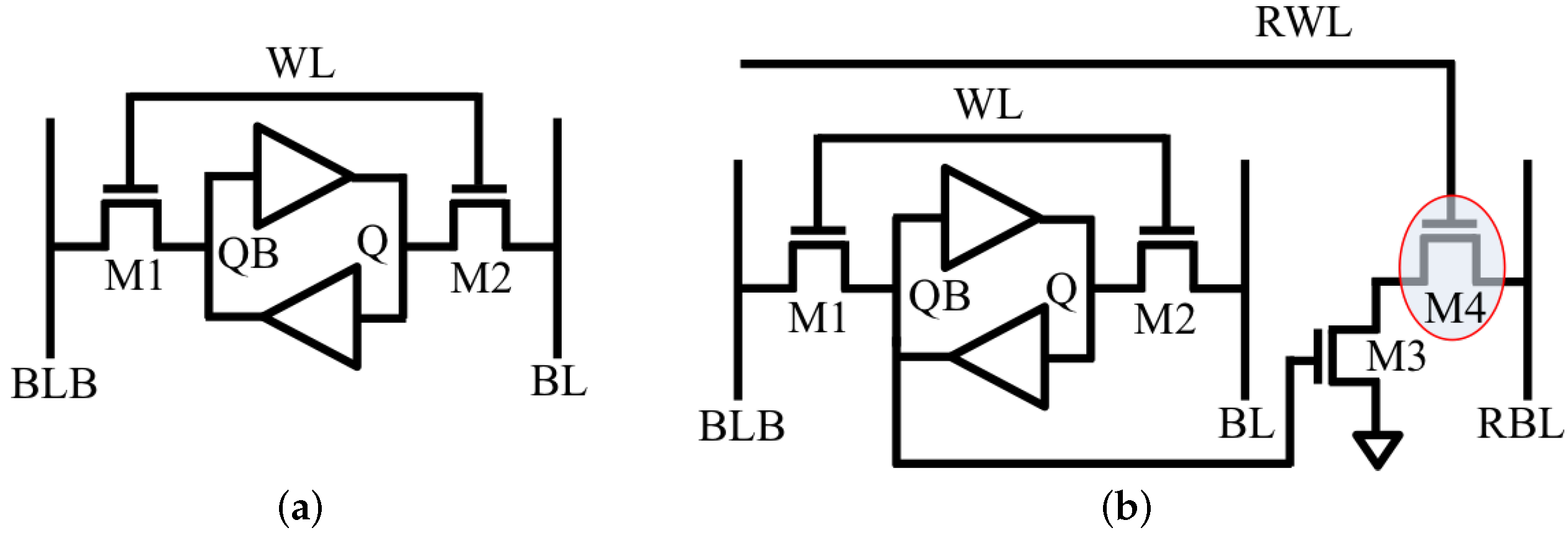
Figure 1. Conventional static random access memory (SRAM) structures. (a) 6T and (b) 8T.
Electronics 08 00611 g001
Figure 2. One column of 32 bit SRAM memory. PC is the control signal for precharging, 32 WLs are the word lines for each row of SRAM, and WBLB is the write bit-line bar and WBL is the write bit line, respectively.
Electronics 08 00611 g002
Figure 3. Layouts of an SRAM bit cell. (a) 6T and (b) 8T.
Electronics 08 00611 g003
Figure 4. Layout of the 32-bit SRAM, one column. (a) 6T and (b) 8T.
Electronics 08 00611 g004
Figure 5. Normalized on- and off-stage current for different channel length (FF corner and 120 °C temperature). They are normalized to the current of the 100 nm channel length.
Electronics 08 00611 g005
Figure 6. Monte Carlo simulation of the cross-coupled inverters to find the trip voltage. (top) The histogram and (bottom) the input (output) voltage values.
Electronics 08 00611 g006
Figure 7. Waveform of read operation in (a) 6T and (b) 8T.
Electronics 08 00611 g007
Figure 8. A bit-line voltage distribution in the Monte Carlo simulation of the reading operation. (a) 6T (b) 8T SRAM with different M4 channel lengths.
Electronics 08 00611 g008
Table 1. Data pattern dependency for leakage current at bit line (BL) (read bit line (RBL) in 8T) when reading the 32th cell.
Best Leakage PatternWorst Leakage Pattern
1∼31th32th1∼31th32th
Q1101
QB0010
Table 2. Transistors size of the 6T and 8T SRAM cell shown in Figure 1 and Figure 3.
TransistorsWidth (nm)/Length (nm)
M1120/60
M2120/60
M3 (8T only)180/60
M4 (8T only)120/60–100 (L varies)
Inverter NMOS180/60
Inverter PMOS120/60
Table 3. Read-error rate of 6T SRAM and 8T SRAM.
Data6T8T8T8T8T8T
Value(L = 60 nm)(L = 70 nm)(L = 80 nm)(L = 90 nm)(L = 100 nm)
‘0’56.5%4.4%5.2%5.3%5.8%5.8%
‘1’10.9%91.9%17.1%0.2%0.0%0.0%
average33.7%48.2%11.2%2.8%2.9%2.9%