1. Introduction
As the feature size of very large-scale integrated (VLSI) circuits is scaled down to the nanometer order, various performance degradation and stability problems on the conventional Cu interconnects have emerged in recent years [
1,
2,
3]. Graphene, as a promising candidate for replacing the common copper, has attracted the intensive interest of many researchers in terms of its excellent electrical, mechanical and thermal properties [
4,
5]. Compared with the copper material, high quality graphene has a long mean free path on the order of several micrometers, which can result in a lower resistivity and achieving the ballistic transport at shorter interconnects. The current density of graphene can reach 10
9 A/cm
2 in comparison to its Cu counterpart, thereby, eliminating the electromigration and skin effect of Cu interconnects [
6]. Graphene nanoribbon (GNR) is a narrow strip of graphene sheet, which can be classified into multilayer GNR (MLGNR) and single-layer GNR (SLGNR) depending on its stacked number of layers. SLGNR is not suitable for on-chip interconnects owing to its larger intrinsic resistance [
7,
8,
9]. Based on the types of connection with other devices or interconnects, MLGNR can be further categorized into top contact MLGNR (TC-MLGNR) and side contact MLGNR (SC-MLGNR) [
10,
11,
12]. TC-MLGNR has only the top most layer connected to surrounding contacts while all layers of SC-MLGNR are coupled with the other contacts, which results in the distributed scattering resistance of the former over the latter. Hence the SC-MLGNR is adopted as interconnect material in this paper.
With the interconnect width shrinking into the nanometer scale, the crosstalk delay, crosstalk noise, and transfer gain of global interconnects in VLSI circuits have become major performance concerns owing to the longer distance. To date, a series of studies about these issues on MLGNR interconnects have been done. In reference [
13], Agrawal et al. presented the analytical model of crosstalk delay and crosstalk noise based on the FDTD method. In references [
14,
15,
16], the propagation delay and transfer gain for a single-line of MLGNR interconnect were investigated. In reference [
17], Sahoo et al. analyzed the characteristic of crosstalk noise of coupled MLGNR interconnects, considering the coupling capacitance. In reference [
1], Zhao et al. analyzed and compared the performance difference of crosstalk noise and crosstalk delay between coupled MLGNR and Cu interconnects, considering the impact of coupling capacitance.
However, the works mentioned above only focus on how to establish the analytical model but do not propose the optimization method to reduce crosstalk delay and crosstalk noise and increase transfer gain of on-chip interconnects. Apparently, it is crucial to further enhance the MLGNR interconnects performance at the end of the roadmap. There are some reports that replacing the SiO
2 with the ultra-low-k dielectric materials (k ≤ 2) as the dielectric medium can reduce the delay of on-chip interconnects [
18,
19,
20,
21,
22]. Hence, it is also necessary to investigate the effects of the ultra-low-k dielectric materials on the crosstalk noise and transfer gain of on-chip interconnects. So far, to the best of our knowledge, there is no research to propose the analytical model of coupled MLGNR interconnects, considering the impact of the ultra-low-k dielectric materials. Therefore, in this paper, an analytical model for crosstalk delay, noise output, and frequency response of coupled MLGNR interconnects with different dielectric materials is proposed.
The overview of development about the ultra-low-k dielectric constant materials is shown as follows. The relative dielectric constant of SiO
2 as the most common insulator material is usually equal to 3.9 [
20]. The low dielectric constant (low-k) SiCOH (k = 3.0) is regarded as an effective substitute for the conventional SiO
2 and has been successfully integrated in some 130 nm and 90 nm VLSI circuits [
21]. The emergence of the porosity fabrication technology by plasma-enhanced chemical vapor deposition (PECVD) can reduce the relative dielectric constant of insulator material [
21]. By applying the fabrication technology, SiCOH is processed into porous p-SiCOH (k = 2.4) that has been applied at IBM’s P7 microprocessor [
21]. With the continuous advancement of the porosity fabrication technology, the inorganic ultra-low-k dielectrics, such as nanoglass, have the relative dielectric constant of 1.3 [
22]. In view of the current research progress of insulator material of VLSI circuits, the nanoglass is the lowest dielectric constant material. Thus, nanoglass was adopted as the ultra-low-k dielectric constant material for analysis of performance of on-chip interconnect compared with the conventional SiO
2 in the paper.
2. Interconnect Model
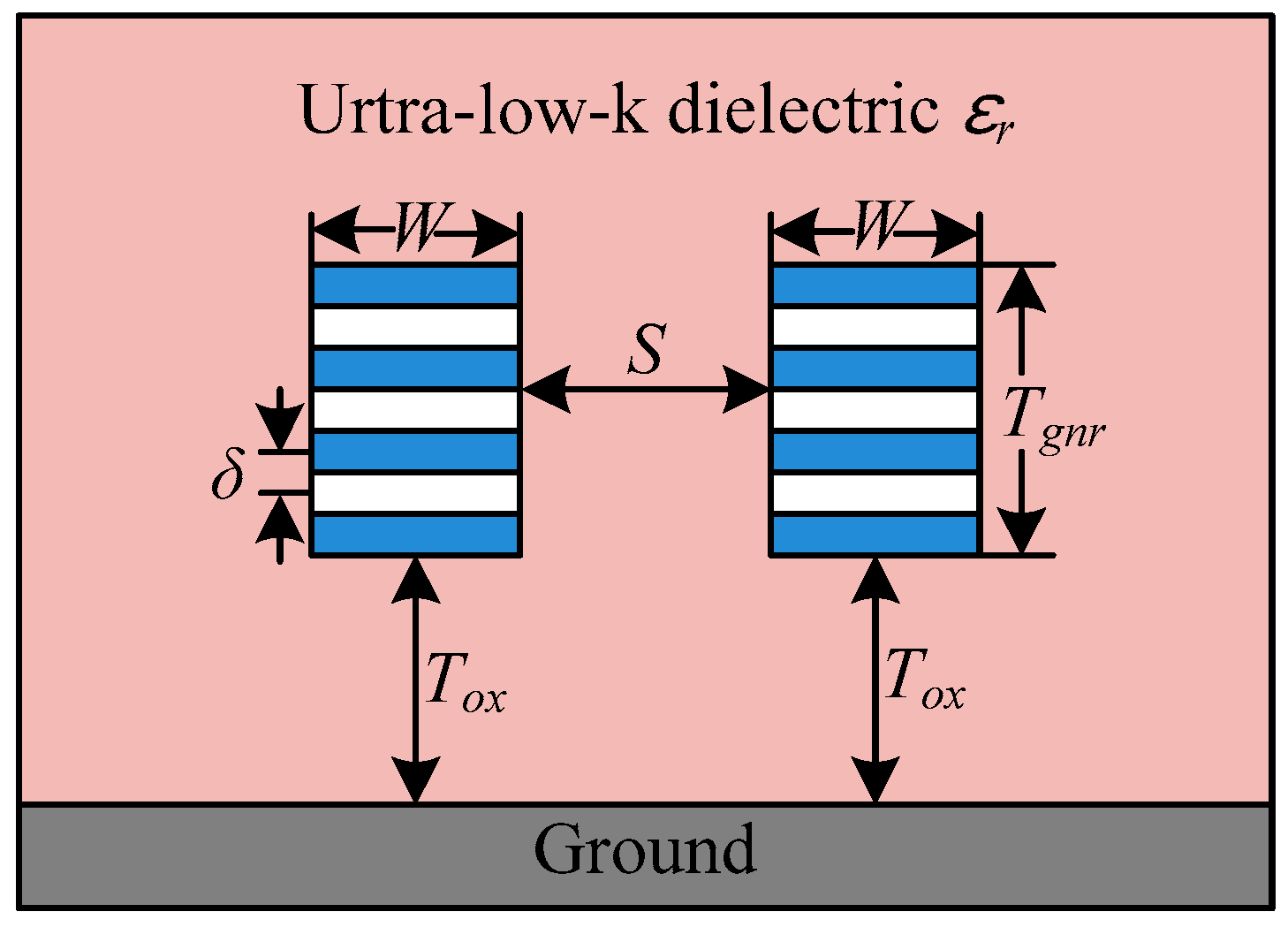
A typical geometry of two-line coupled MLGNR interconnects placed above the ground plane and surrounded by a dielectric medium is exhibited in
Figure 1, where the common SiO
2 dielectric material is replaced by the ultra-low-k dielectric material. The
W,
S,
Tgnr,
Tox, and
εr are line width, line space, line height, thickness of insulator dielectric, and relative dielectric constant of the ultra-low-k dielectric material, respectively. The total number of layers for MLGNR depends on the line thickness
Tgnr and can be expressed as
Nlayer = 1 + Integer[
Tgnr/
δ] [
23]. Herein the operator Integer[.] means that only the integer part is considered and
δ (=0.34 nm) is the interlayer spacing between successive GNR layers [
24].
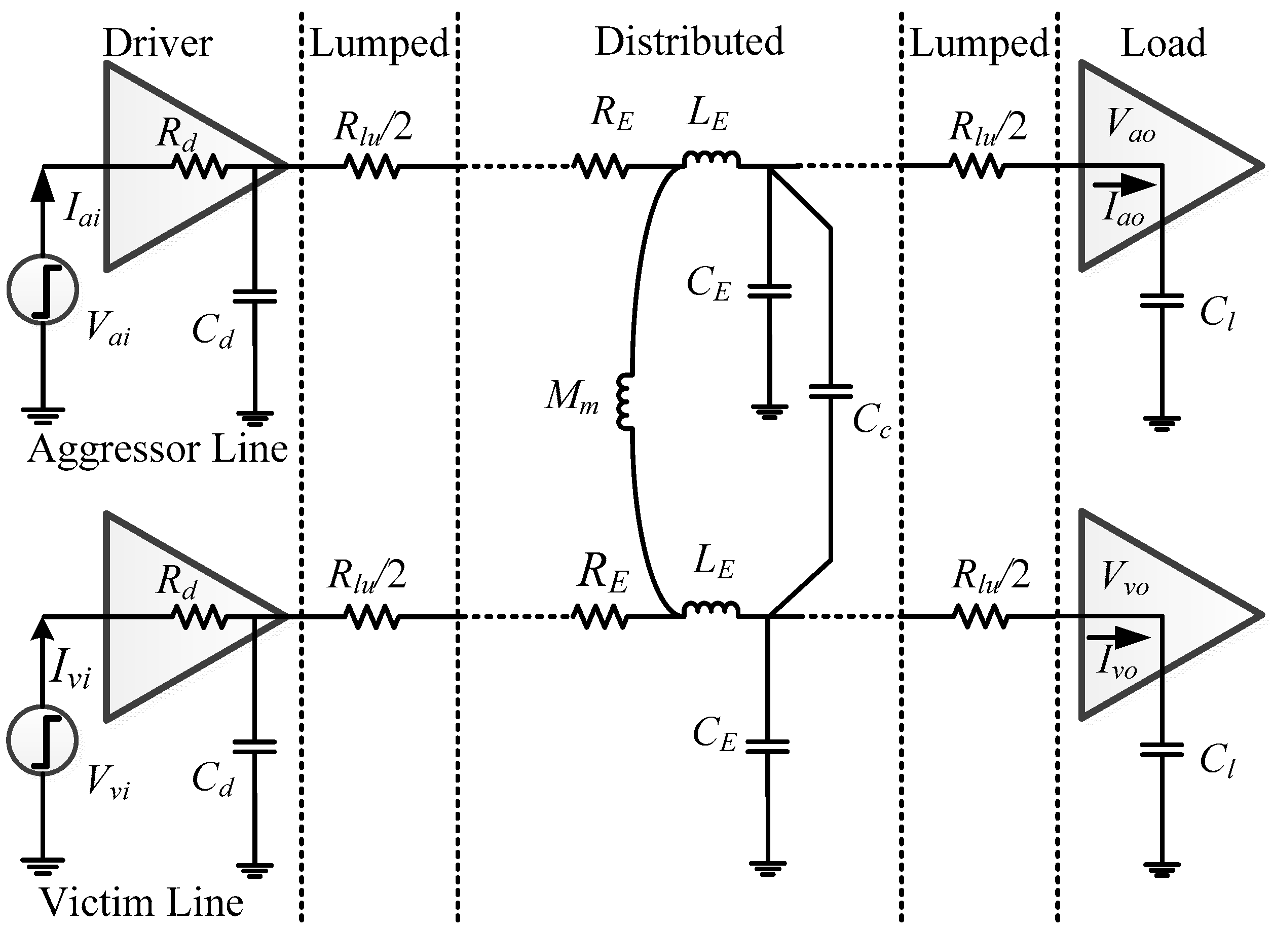
As shown in
Figure 2, the equivalent circuit model for two-line coupled MLGNR interconnects is configured with the same effective driver resistance
Rd, driver capacitance
Cd, and load capacitance
Cl for aggressor and victim lines. The coupled MLGNR interconnects are comprised of lumped and distributed parts.
For MLGNR coupled interconnects,
Rlu and
RE represent the lumped resistance and per unit length (p.u.l.) equivalent distributed scattering resistance, respectively. They can be given by [
7],
Here,
Rcm denotes the imperfect contact resistance and its value ranges from 1 KΩ to 20 KΩ [
13].
Rqm is the monolayer quantum resistance and can be defined as
Rqm =
h/2
e2 (herein
h is Plank’s constant and
e is charge of electron).
λeff denotes the effective mean free path (MFP).
Nch represents the total number of conducting channels in the monolayer GNR and can be approximated as below [
25,
26],
where
a0 to
a5 are the parameters for zigzag MLGNR (zz-MLGNR) at room temperature (300 K) with the Fermi energy
EF over 0 [
25]. In the light of the total number of conducting channels of zigzag MLGNR over armchair MLGNR (ac-MLGNR), hence, only the zz-MLGNR is investigated in the paper.
Lgnr represents the length of MLGNR interconnects. The effective mean free path (MFP) for the
ith-subband can be expressed as,
Herein,
λd represents the mean free path due to the scattering effects by the static impurities and crystal defects (=1 µm) [
1,
10].
λs denotes the mean free path induced by electron–phonon scattering (=70 μm) [
27].
λe,i is the mean free path contributed to the scattering of edge roughness, which is depended on the interconnect width and the backscattering probability
P at the edges [
28].
where
vf is the Fermi velocity of electrons in graphene (=8 × 10
5 m/s) [
12]. The value of
P will change when the edge roughness situation is different. Especially,
P = 0 and
P = 1 demonstrate that the edge of MLGNR are fully specular and fully diffusive, respectively [
1].
The distributed capacitance
CE of MLGNR interconnects comprises of the equivalent quantum capacitance
Ceq and the electrostatic capacitance
Cel. The p.u.l. equivalent quantum capacitance can be obtained by using a recursive scheme as [
1,
7,
17],
wherein,
Cq is the p.u.l. length quantum capacitance of monolayer GNR.
Cm is the p.u.l. coupling capacitance between successive GNR layers and can be defined as
Cm =
ε0W/
δ (here
ε0 = 8.854 × 10
−12 is the vacuum dielectric constant). In order to investigate the impacts of ultra-low-k dielectric material materials, thus the relative dielectric constant
εr can be applied to distinguish different dielectric mediums in this paper. The p.u.l. electrostatic capacitance
Cel is determined by the interconnect dimension and relative dielectric constant
εr of medium material, and can be derived as [
29],
where
M [.] can be described as [
30],
Therefore, the p.u.l. distributed capacitance
CE can be calculated as,
The distributed inductance
LE of MLGNR interconnects consists of the equivalent kinetic inductance
Leq and magnetic inductance
Lma, and their relationship can be described as in Equation (12). Similarly, the p.u.l. equivalent kinetic inductance
Leq also can be computed by using a recursive method as [
1,
17],
Herein, Lk represents the p.u.l. kinetic inductance of monolayer GNR. Lm denotes the p.u.l. coupling inductance between successive GNR layers and can be expressed as Lm = µ0δ/W (here µ0 = 8.854 × 10⁻¹² is the vacuum magnetic permeability).
As illustrated in
Figure 2, the impacts of mutual inductance
Mm and coupling capacitance
Cc on the dynamic and functional crosstalk of the coupled MLGNR interconnects are taken into consideration. The analytical expressions of p.u.l.
Mm and
Cc are defined as follows [
13],
Herein
C[BCP](
z, y) and
C[CP](
z) are written as below,
wherein the function
M [.] is shown in Equation (10),
K[BCP](z,y) and
K[CP](z) are given in reference [
30].
3. Crosstalk Delay Model
Based on the single-line delay model [
31], we derived a 50% crosstalk delay model of the coupled MLGNR interconnects considering the in-phase crosstalk and out-of-phase crosstalk as,
Here, the total equivalent capacitance CT = CE + (1 − β)Cc, the total inductance LT = LE + βMm and .
The dynamic crosstalk consists of in-phase crosstalk and out-of-phase crosstalk schemes. For the switching factor β, β = 1 and β = −1 are introduced to distinguish the corresponding schemes, namely, the aggressor and victim lines switching in the same direction and opposite direction, respectively.
4. Crosstalk Noise Model
The ABCD parameter matrix for the MLGNR victim interconnect excluding the driver and load terminals under in-phase crosstalk and out-of-phase crosstalk schemes, respectively, can be expressed as,
where
θin and
θout are propagation constant of the MLGNR victim interconnect under in-phase crosstalk and out-of-phase crosstalk models, respectively. Similarly,
Zin and
Zout represent the corresponding characteristic impedance, respectively. They are given by,
Herein θ(in,out) is composed of θin and θout cases, similarly, Zin and Zout are expressed as Z(in,out). β = 1 is for the in-phase crosstalk scheme while β = −1 represents the out-of-phase crosstalk case.
Taking the effect of the driver terminals into account, the total ABCD parameter matrix of the MLGNR victim interconnect at different crosstalk models can be written by,
Being similar to the situation mentioned above (
θ(in,out) and
Z(in,out)),
AT(in,out) consists of
AT(in) and
AT(out) cases, which represents the parameters of the total ABCD matrix under in-phase crosstalk and out-of-phase crosstalk models. The meaning of parameters
BT(in,out),
CT(in,out), and
DT(in,out) are the same as the
AT(in,out) that contain two cases of in-phase crosstalk and out-of-phase crosstalk
. They can be solved by matrix computation as follows,
Combining the total ABCD parameter matrix described in Equation (25), the relationship between the voltage and current of input–output ports for the MLGNR victim interconnect depicted in
Figure 2, can be deduced as,
Substituting the expression of load capacitance
Ivo =
sClVvo shown in
Figure 2 into Equation (26), the transfer functions of the decoupled MLGNR victim interconnect under different phase modes are derived as,
Herein, in order to ensure the signal integrity characteristics at the output port of MLGNR victim interconnect, the transfer functions are approximated by adopting a fifth-order pade’s expansion.
The crosstalk noise is usually defined as the functional crosstalk. It can be defined that the aggressor line switches from logic 0 to logic 1 while the victim line keeps in a quiescent state of logic 0. Based on the principle of the functional crosstalk, a peak voltage will be observed at output port of the victim line when the aggressor line switches owing to the coupled crosstalk. The noise output of the MLGNR victim interconnect induced by the switching of aggressor line can be obtained as follows [
32],
where
Vnoise(
s) represents the noise output signal of the MLGNR victim interconnect in the Laplace domain. Here the input port of MLGNR aggressor line is defined into an ideal step-response signal
Vagg(
s) = 1/
s. We can obtain the noise output signal in the time domain by applying the inverse Laplace transform for the Equation (29) as,
5. Results and Discussions
This section investigates the impacts of different dielectric materials on crosstalk delay, transfer gain, and noise output signal of coupled MLGNR interconnect at global level of 7 nm technology node. All geometrical and physical electrical parameters were extracted from references [
33,
34] as follows,
W = 11.5 nm,
Tgnr = 26.91 nm,
S = 11.5 nm,
Tox = 17.25 nm,
Ef = 0.3 eV,
ε0 = 1.95 × 10
−11 F/m,
µ0 = 4π × 10
−7,
P = 0,
Rd = 20.51 kΩ,
Cd = 0.063 fF,
Cl = 0.2 fF. Herein,
Rd,
Cd, and
Cl are the equivalent values of minimum-sized gate. In general, the sizes of driver and load are 100 times larger than that of the minimum-sized gate at global level (100 µm ≤
Lgnr ≤ 10 mm) interconnects [
35], then their values can be rewritten as,
Rd’ =
Rd/100,
Cd’ =
Cd × 100 and
Cl’ =
Cl × 100. All the numerical simulation results presented in the next section were obtained by carrying out the MATLAB R2013a.
In order to compare the impacts of different dielectric mediums on delay time of coupled MLGNR interconnect, the crosstalk delay of victim line versus interconnect length under different phase modes were obtained by the Equation (20), as displayed in
Figure 3.
As shown in
Figure 3, it can be observed that the crosstalk delay for the coupled MLGNR interconnect with the nanoglass (
εr = 1.3) as the dielectric medium is less than that of the conventional SiO
2 dielectric medium under in-phase and out-of-phase modes. Taking the interconnect length of
Lgnr = 2000 µm as an instance, the delay time under out-of-phase mode for the nanoglass medium is 6.886 ns while for the SiO
2 dielectric medium is 18.115 ns. Similarly, the delay time at in-phase mode for nanoglass and SiO
2 dielectric mediums are 2.277 ns and 4.286 ns in the same length as the former, respectively. The reason behind this is that the electrostatic capacitance and coupling capacitance will reduce as the relative dielectric constant
εr decrease, thereby, leading to a lesser total equivalent capacitance
CT. In combination with Equation (20), it is evident that the crosstalk delay is approximately in positive proportion with the total equivalent capacitance
CT. In addition, according to our numerical simulation results, the maximum difference of delay time between SiO
2 and nanoglass dielectric mediums can reach to 25.202 ns for an interconnect length of
Lgnr = 3000 µm at the out-of phase crosstalk. Thus, replacing the traditional SiO
2 with the ultra-low-k dielectric material is an efficient way to reduce crosstalk delay of coupled interconnects.
Moreover, it is clearly shown from
Figure 3 that the crosstalk delay of coupled MLGNR interconnects at out-of-phase mode is significantly higher than that of in-phase crosstalk mode for all dielectric materials. Giving the interconnect length of
Lgnr = 2500 µm as an example, the delay time for SiO
2 dielectric medium under in-phase and out-of-phase modes are 6.308 ns and 27.883 ns. The corresponding values for p-SiCOH dielectric medium are 4.525 ns and 17.802 ns, and the case for nanoglass dielectric medium are 3.173 ns and 10.364 ns. This can be explained by the Miller coupling capacitance, which only exists in out-of-phase crosstalk mode, causing the total equivalent capacitance of the MLGNR victim interconnects under out-of-phase mode to be greater than that of in-phase mode.
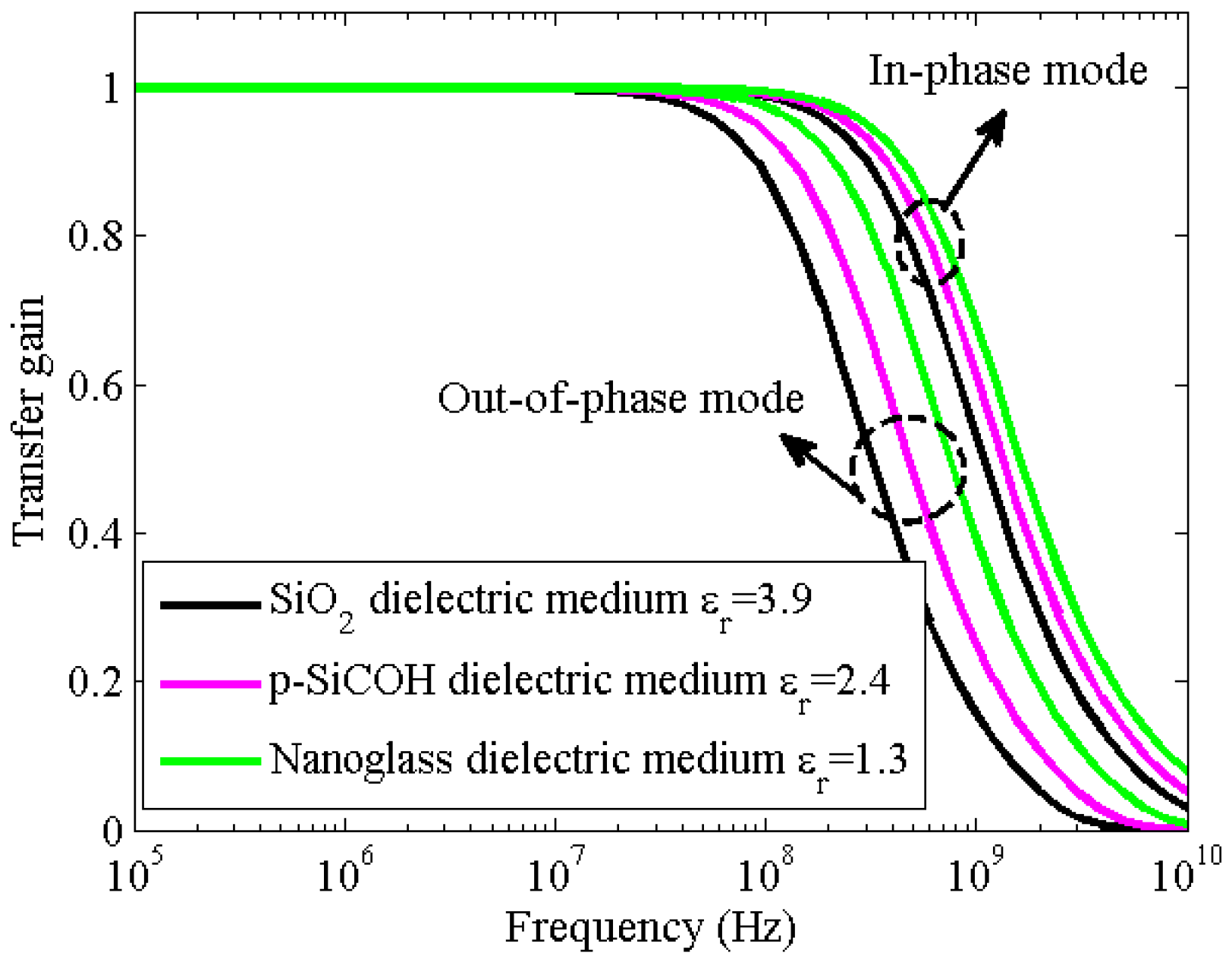
Figure 4 shows the frequency response of MLGNR victim line with the interconnect length
Lgnr = 1000 µm under in-phase and out-of-phase modes for different dielectric materials. Transfer gain represents the magnitude of frequency response of the interconnect system and is the ratio of amplitude between the output and input signal at different frequencies. The transfer gain under in-phase and out-of-phase can be obtained by the Equations (27) and (28), respectively. As shown in
Figure 4, in the high frequency region, it is obvious that the transfer gain increases as the relative dielectric constant
εr decreases for in-phase and out-of-phase modes. This is due to the fact that the coupled MLGNR interconnects system can be considered as the RC low pass filter and its cut-off frequency is approximately expressed as: 1/(2π ×
CT ×
RE) [
16], and the total capacitance
CT of the victim line decreases with the decrease of
εr. Thus the MLGNR victim interconnect for using the nanoglass has a larger cut-off frequency compared with the p-SiCOH and SiO
2 cases.
Moreover, it can be found from
Figure 4 that transfer gain of coupled MLGNR interconnects under in-phase mode is evidently greater than that of out-of-phase crosstalk mode for any dielectric materials. The reason for this phenomenon is that the total capacitance of the victim MLGNR interconnect under out-of-phase mode is larger than that of in-phase mode. Therefore, the former will have a lesser cut-off frequency compared with the latter.
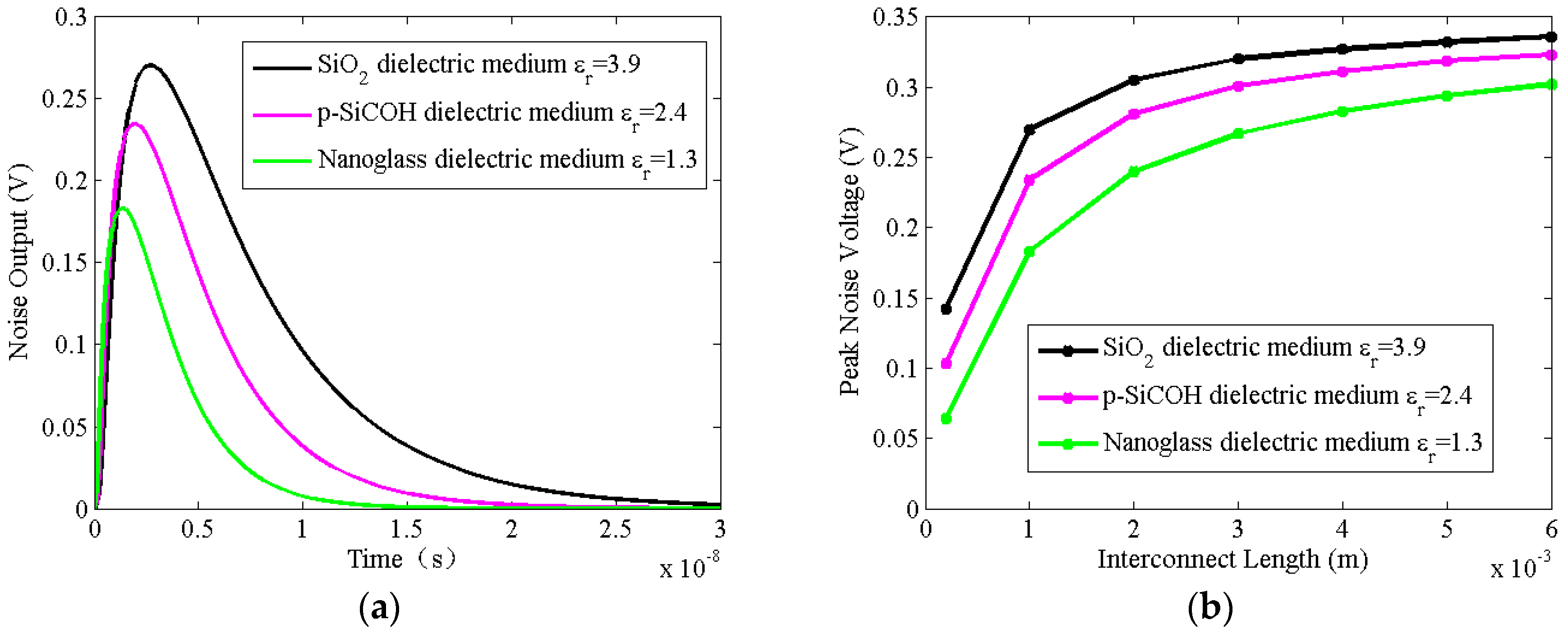
Based on the Equation (30), the effect of different dielectric mediums on crosstalk noise of victim MLGNR interconnect is illustrated in
Figure 5a, meanwhile the peak noise voltage regarding the indispensable noise parameter for different dielectric mediums versus interconnect length is described in
Figure 5b.
It is remarkable from
Figure 5a that the peak noise voltage will decrease with the decrease of the relative dielectric constant
εr. For instance, the peak noise voltage with the interconnect length
Lgnr = 1000 µm for SiO
2, p-SiCOH and nanoglass dielectric mediums are 0.270 V, 0.234 V, and 0.183 V, respectively. It can be explained that the crosstalk noise is induced by the coupling capacitance
Cc and mutual inductance
Mm existing on the position between aggressor and victim MLGNR interconnect, as shown in
Figure 2. On the other hand, it is noteworthy that the Miller coupling capacitance is the dominant factor of forming the crosstalk noise. Certainly, there is no doubt according to the Equations (17)–(19) that a lesser relative dielectric constant
εr can result in a smaller Miller coupling capacitance.
Moreover, as shown in
Figure 5b, it is obviously found that the peak noise voltage of coupled MLGNR interconnect increases as the interconnect length increases for all different dielectric mediums. This is due to the fact that the increases of interconnect length give rise to Miller coupling capacitance. In addition, it is shown from
Figure 5b that applying the ultra-low-k dielectric material to reduce the peak noise voltage is very obvious at global level interconnects. Based on the numerical simulation results, the maximum difference of peak noise voltage between the SiO
2 and nanoglass dielectric mediums can reach to 0.102 V when the interconnect length
Lgnr = 1000 µm, and the corresponding value for the minimum difference is 0.038 V when the interconnect length is chosen as
Lgnr = 6000 µm.

