Article

High-Performance Time Server Core for FPGA System-on-Chip

Electronics Technology Department, E.T.S. Ingeniería Informática, University of Seville, Avda. Reina Mercedes s/n, 41012 Seville, Spain
*
Author to whom correspondence should be addressed.
Electronics 2019, 8(5), 528; https://doi.org/10.3390/electronics8050528
Submission received: 11 April 2019 / Revised: 3 May 2019 / Accepted: 7 May 2019 / Published: 11 May 2019
(This article belongs to the Special Issue New Applications and Architectures Based on FPGA/SoC)

Abstract

:
This paper presents the complete design and implementation of a low-cost, low-footprint, network time protocol server core for field programmable gate arrays. The core uses a carefully designed modular architecture, which is fully implemented in hardware using digital circuits and systems. Most remarkable novelties introduced are a hardware-optimized timekeeping algorithm implementation, and a full-hardware protocol stack and automatic network configuration. As a result, the core is able to achieve similar accuracy and performance to typical high-performance network time protocol server equipment. The core uses a standard global positioning system receiver as time reference, has a small footprint and can easily fit in a low-range field-programmable chip, greatly scaling down from previous system-on-chip time synchronization systems. Accuracy and performance results show that the core can serve hundreds of thousands of network time clients with negligible accuracy degradation, in contrast to state-of-the-art high-performance time server equipment. Therefore, this core provides a valuable time server solution for a wide range of emerging embedded and distributed network applications such as the Internet of Things and the smart grid, at a fraction of the cost and footprint of current discrete and embedded solutions.

1. Introduction

Network time synchronization allows the nodes in a distributed system to share a common time through exchanging time synchronization packets with one or more reference nodes (the time servers). Time synchronization is recognized as a key component in all types of distributed systems, such as worldwide Internet services, industrial data acquisition systems [1], power distribution [2] and Internet of Things (IoT) applications [3]. Synchronization accuracy requirements are very dependent on the application field and particular tasks. Industrial and smart grid applications commonly require 1 μ s to 100 ms accuracy, whereas mobile networks, audio-video transmission and measurement applications normally aim at sub-microsecond accuracy [4].
Several synchronization algorithms over communication networks have been proposed by the scientific community with different levels of complexity and precision. Nowadays, the two main network synchronization protocols are network time protocol (NTP) [5], and IEEE 1588 precision time protocol (PTP) [6]. Both define various accuracy categories among their servers, with stratum-1 servers (NTP) or master clocks (PTP) being the most accurate references in the network. These top-level time sources are usually high-performance discrete synchronization servers from several manufacturers [7,8,9,10] that use an external time reference, such as global positioning system (GPS) [11], as a time source. These synchronization servers commonly support both protocols and employ dedicated hardware to handle the critical task of timestamping synchronization packets. Synchronization servers also achieve an accuracy to the reference from 1 μ s to a few milliseconds, with a maximum request ratio from 1000 to 10,000 requests per second, according to manufacturers specifications [8,9,10]. This exactitude and performance amounts an average cost that ranges from $ 3000 to $10,000 as of 2019.
A dedicated discrete synchronization server may be a good solution for large and centralized infrastructures as found in the telecommunications industry. However, cost, size and/or power consumption render these systems inadequate for most embedded and highly distributed applications. Since a massive adoption of highly distributed technologies, such as the IoT, is expected in the forthcoming years [12], several authors have proposed NTP and PTP servers and/or clients solutions from the embedded systems perspective, frequently implemented as a system-on-chip (SoC) on a field programmable gate array (FPGA) device.
Software-only embedded implementations are cheaper and easier to develop. Nevertheless, these solutions can only provide limited accuracy (e.g., embedded NTP implementations in [13,14]) report an accuracy in the range of several milliseconds, whereas other approaches based on the advanced RISC machine (ARM) architecture [15,16] are close to 1 ms). Similarly, the software-only PTP system in [17] reports an accuracy from 10 μ s to 200 μ s, depending on the server load. To approach to limited-resource systems, such as numerous IoT applications, less accurate techniques [18] must be applied instead of complex protocols, such as NTP or PTP.
In contrast, hardware-assisted embedded approaches are more difficult to develop and have the extra cost of the dedicated hardware, although the expansion of FPGAs and modern FPGA-based SoC platforms have greatly dropped the cost barrier in the last few years. Hardware-assisted solutions aim to sub-microsecond accuracy in order to cope with more demanding applications, such as audio-video data synchronization [19], smart grid control [20] or high-accuracy data acquisition [21].
This contribution goes one step forward by developing an NTP server core for FPGA completely elaborated in hardware that handles both the timekeeping functions and network communications, and can operate stand-alone or embedded in a SoC. The NTP core provides highly distributed applications with a complete time server synchronization solution at a lower size and cost than previously developed SoC-based time synchronization systems (see Figure 1). It means that the full functionality of an NTP server can be embedded as a module in any FPGA-based system, while offering an accuracy and performance comparable to that found in large and expensive high-performance NTP servers.
The rest of the paper is organized as follows. Section 2 presents previous and related work, Section 3 introduces the NTP protocol and Section 4 offers an overview of the structure and operation of the core. Section 5 and Section 6 detail design and implementation. Accuracy and performance results are presented and discussed in Section 7 and the main conclusions are summarized in Section 8.

2. Previous and Related Work

2.1. Previous Work

The authors have done research on accurate hardware-based time synchronization since 2007. A fully-hardware NTP client is first introduced in [22,23] with application to industrial remote terminal units (RTU). Further development in hardware-oriented clock discipline algorithms is presented in [24] allowing for better accuracy and performance. Later on, the authors started working in a more flexible and general purpose modular hardware architecture for NTP client and server development. An overview of the new architecture is introduced in the summary of a conference’s invited talk in [25], together with some preliminary performance estimations derived from early, functionally-incomplete prototypes.
This paper is the evolution of the initial architecture applied to the development of a general-purpose fully-functional NTP server. Detailed description of the the architecture and its building blocks is offered here for the first time, together with up to date extensive performance results.

2.2. Related Work

In recent years, several time synchronization systems have been proposed from the embedded systems perspective, using the flexibility of the FPGA platform. Some of these approaches are commented on below.
Software-only NTP implementations in [13,14] generate a clock signal with an accuracy in the range of several milliseconds with respect to the time reference. This accuracy is far from the range of 1 μ s of typical NTP equipment. Other software implementations based on the ARM architecture can be found in [15,16]. The accuracy reported in [15] is in the range of the expected accuracy of 1 ms typical of software-only NTP servers, even though a voltage controlled temperature compensated crystal oscillator (VCTCCO) is used to improve the accuracy of the local clock. The authors of [16] basically did a port of the standard NTP server software to their ARM-based development platform and did not report any experimental results.
Regarding the full hardware NTP client/server in [19], it is designed on a low-cost FPGA chip integrated with an oven controlled crystal oscillator (OCXO). The implementation is not described in detail. Results show a high degree of accuracy in the pulse-per-second (PPS) signal generated by the server and a synchronized NTP client (below 5 μ s). However, the accuracy of the NTP server’s PPS signal with respect to its time source (GPS receiver) is not reported. It is also not clear if the protocol used is the standard NTP or an NTP variant implemented on top of Ethernet without the internet protocol (IP) level.
Moreira et al. [20] developed various PTP client and server implementations for the Xilinx Zynq-7000 platform. This platform includes both programmable logic and an ARM processor. The authors followed the hardware–software SoC approach by using dedicated synchronization hardware tied to the Ethernet controller together with PTP software running on the Linux operation system. Results obtained by connecting client and server through a single Ethernet link (no switch in the middle) report an offset error of 40 ns, while network tests are below 1 μ s.
A similar approach comes from the White Rabbit (WR) Project [26]. The WR Project aims at sub-nanosecond accuracy by using extensions to the PTP and Ethernet protocols. The system proposed in [21] uses a mixed software–hardware approach that combines FPGA-based specific hardware together with controlling software running in an ARM microprocessor. The whole system is implemented as a SoC using the Xilinx’s Zynq development platform. The result is a stand-alone WR node that should be able to achieve nanosecond accuracy when used inside the very specialized WR ecosystem.
Table 1 offers a quick overview of the commented related work.
When compared to other author’s related work, the approach used in this paper has the following advantages:
  • Scale: The system is a very small core compared to previous SoC approaches, and can be used stand-alone or integrated in any other SoC project.
  • Hardware-only: It does not require a software stack or even a processor and associated resources, allowing for very efficient operation in both performance and power consumption.
  • Standard logic design: It can be easily ported to any platform with a minimum effort, and does not need any additional external devices to operate.
  • The cores uses a modular design that can be extended and/or reused to tackle other applications: use of other protocols, client design, etc.
In summary, this contribution tries to fill an important niche: producing a very low-footprint embedded time server solution that is as accurate as discrete commercial equipment, with minimum hardware requirements and synthesizable on standard digital programmable logic. Compared to previous SoC-scale approaches, the proposed design is more suited to fulfill the cost, performance and efficiency demands of the IoT field.

3. NTP Synchronization

The NTP synchronization protocol is based on exchanging packets between clients and servers. This mechanism is called on-wire protocol and aims to determine the offset of the client’s local clock, with respect to the server’s clock, and the latency of the network connection. Figure 2 describes the operation of the NTP on-wire protocol. The client sends a request to the server by issuing an user datagram protocol (UDP) data packet including the time at its local clock T 1 (origin timestamp). A new time T 2 is registered with the reception time as given by the server’s local clock (receive timestamp) when the request is received at the server. After processing the request, the server issues a reply including the time at which the reply leaves the server T 3 (transmit timestamp). As soon as the client receives the reply, the arrival time T 4 is also annotated (destination timestamp). This set of timestamps help the client calculate the round trip time ( δ ) and the time offset between the server’s and the client’s clocks ( θ ). Assuming a symmetric connection (equal delay in both directions), these times can be calculated as:
δ = ( T 4 T 1 ) ( T 3 T 2 ) θ = ( T 2 T 1 ) + ( T 3 T 4 ) 2
The client can correct its local clock to match the server’s time as accurately as possible using the clock offset, the round trip delay and additional statistical measurements based on the calculated offset and delay. Software implementations of NTP clients normally achieve time synchronization accuracy within a millisecond with respect to NTP servers on the Internet [27]. There are two main sources of error that could limit the accuracy. The first one is asymmetry in the network communication when time spent by the client’s request to reach the server differs from time spent by the server’s response to reach the client. This asymmetry is due to various latencies found in network paths and in network equipments. While the PTP is able to compensate for systematic known latency asymmetry [28], NTP does not provide any standard compensation mechanism. The second main source of error comes from the variable latency between the instant in which the timestamp is registered in the datagram, and the real instant the datagram leaves or reaches the host. However, in common software implementation, these timestamps are registered by client/server software running as a user level application. Therefore, the timestamp error will depend on time spent processing the datagram, as it goes through the protocol stack and software layers. Hence, this error will largely depend on system load and detailed software implementation.
The NTP implements a set of advanced algorithms in order to mitigate these errors and improve accuracy [5]. In a first stage, the NTP client sends requests to multiple servers and the algorithm calculates offset ( θ ), delay ( δ ), dispersion ( ϵ ), and jitter ( φ ) for every server. Dispersion represents the maximum error due to the frequency tolerance and time spent since the last packet was sent. The jitter is defined as the root-mean-square (RMS) average of the most recent offset differences, representing the nominal error in estimating the offset. While jitter is rarely considered a major factor in ranking server quality, this parameter is a valuable indicator of timekeeping performance and network congestion state.
In a second stage, these data are processed by the mitigation algorithms consisting of selection, clustering, combination and clock discipline. First, the selection algorithm scans all associations and casts off the falsetickers, which have demonstrably incorrect time, leaving the truechimers as a result. Second, in a series of rounds, the clustering algorithm discards the associations statistically furthest from the centroid, until a specified minimum number of survivors remain. Third, the combination algorithm produces the best and final statistics on a weighted average basis, and the best time offsets are obtained. Finally, the clock discipline algorithm is applied to calculate the needed time and frequency corrections in order to match the server’s time as accurately as possible and maintain a stable clock frequency.
The precision of the NTP synchronization can be largely improved by executing the timestamping operation in lower layers [29]. However, to achieve the highest precision in the timestamping operation, the Ethernet network interface card (NIC) must carry out this task as soon as the packets arrive or leave the interface. Therefore, accuracy in the client’s clock can be within one microsecond [29]. This way, the precision of an NTP client/server system can be similar to that of a PTP systems, where hardware-assisted timestamping is mandatory in a standards-compliant implementation.
In addition to the NTP specification, there exists the simple network time protocol (SNTP) specification [30]. Both specifications share the same communication protocol and data format. However, NTP uses sophisticated algorithms described above that ensure a correct synchronization with multiple servers under highly variable latency data links, which is common in a worldwide network such as the Internet. By contrast, SNTP covers the synchronization with a single reference (as happens in Stratum 1 servers) and allows the peers to use simplified stateless algorithms in clients and servers, being better suited to be implemented in embedded systems. Regardless, any NTP or SNTP client will communicate seamlessly with either a SNTP or a full NTP server.

4. NTP Server Core Overview

The NTP server core described in this paper synchronizes with a single reference, a GPS receiver, and operates as a primary (Stratum 1) server following the SNTP. The core can be used in the standard scenario depicted in Figure 3, where the NTP server provides NTP clients in local or remote networks with an NTP synchronization service. Moreover, a configuration server delivers networking configuration parameters (IP address, network mask and so on) to hosts in the network. The configuration server has been explicitly included in that figure since the NTP server core can obtain internal configuration parameters from the configuration server, in addition to the normal network parameters. Consequently, the complete configuration for any number of NTP servers can be maintained in a central place and can be easily updated, even at run-time, if necessary. In particular, the bootstrap protocol (BOOTP) [31] is used for configuration due to its simplicity compared to the dynamic host configuration protocol (DHCP). In fact, most DHCP services also implement the BOOTP, therefore, in most cases, the configuration requirements of the NTP core can be solved by utilizing existing infrastructure.
The NTP server has been designed as a pure digital core requiring a minimum set of external elements (see Figure 4): (i) A physical layer adapter (PHY) that interfaces to the media access control (MAC) controller in the server through the media-independent interface (MII); and (ii) A recommended standard 232 (RS-232) transceiver to convert the output voltage level of the GPS receiver into the appropriate level at the core, if necessary. Such core also uses the pulse per second (PPS) signal from the GPS receiver as well as an optional external digital clock signal (osc), used as the base frequency referencefor the local clock. The server also outputs its local clock time and internal PPS reference (signals local_time and PPSout, respectively) that can be used for testing as well as for delivering accurate time to nearby cores and systems.
Internally, the NTP core consists of five main modules connected as depicted in Figure 5. The MAC controller and the universal asynchronous receiver-transmitter (UART) are standard modules that handle the communication with the Ethernet local network and serial port, respectively. The modules in the NTP core can be grouped into two subsystems: (i) The timekeeping subsystem, formed by the UART, the time reception module and the synchronization module; And (ii) communications subsystem, formed by the comprising protocol and configuration interface (P&CI), and the MAC controller. In the former, the time reception module processes the data received from the GPS unit through the UART and sends the information to the synchronization module, which uses it to maintain the local clock synchronized with the GPS time. In the latter, the P&CI handles the initial configuration of the system and network communications, by means of various Internet protocols, using the MAC controller as the lower-level network interface.
The NTP server core architecture is based on the general NTP server architecture proposed in [25]. Both the synchronization module and the P&CI borrow some ideas and characteristics from some of the modules in the NTP client prototypes in [22,23]. However, the modules in the NTP server core constitute a new server-oriented implementation with greatly extended and improved functionality.
In general, the system operates as follows: upon startup, the P&CI enters the configuration phase and sends a BOOTP request to the network through the MAC controller. The BOOTP response brings back the configuration of the core that the P&CI distributes to the corresponding modules. Thereafter, the system starts normal operation. One of the key aspects of the design is that, once initialized, the timekeeping subsystem works independently of the communication subsystem. On the one hand, the active edge of the PPS signal triggers the reception of the data received from the GPS in the time reception module, collected through the UART. This information is processed and the current time is extracted and handed to the synchronization module, which uses the GPS time and the active edge of the PPS signal to adjust and discipline the local clock. On the other hand, the P&CI waits for NTP requests from clients in the network and, upon reception of an NTP request, an NTP response is built using the local time from the synchronization module. Afterwards, the NTP packet is passed to the MAC controller for delivery.
Splitting tasks between the two subsystems allows the accuracy of the local clock time to be conserved independently of the network load. At the same time, the timekeeping operations triggered by the PPS signal do not affect the NTP network operations carried out by P&CI. This fact contributes to maintaining a constant latency when processing NTP requests, which is vital to minimize errors in the synchronization of clients, as mentioned in Section 3.
The NTP server core uses standard synchronous digital design techniques and it has been optimized to be implemented in low-density cost-effective FPGA chips, and to be able to achieve microsecond accuracy at a system clock frequency as low as 50 MHz. The NTP server core has been implemented in a Xilinx XC3S500E FPGA chip [32]. This low-range and slightly outdated chip has been intentionally selected to demonstrate the performance of the core, even in modest hardware. Most modules in the core implement a control unit described in a hardware description language (HDL) that controls a processing data path. Xilinx System Generator for digital signal processor (DSP) [33] has been utilized to implement some of the data processing blocks, so as to shorten the design time. However, the design can be easily ported to any other platform provided that basic arithmetic and system-level blocks are available. Additionally, the modularity of the design allows the future re-usability of the main blocks depicted in Figure 5 in other synchronization applications.
The next sections further describe the design and operation of the NTP server core’s building blocks.

5. Timekeeping Subsystem

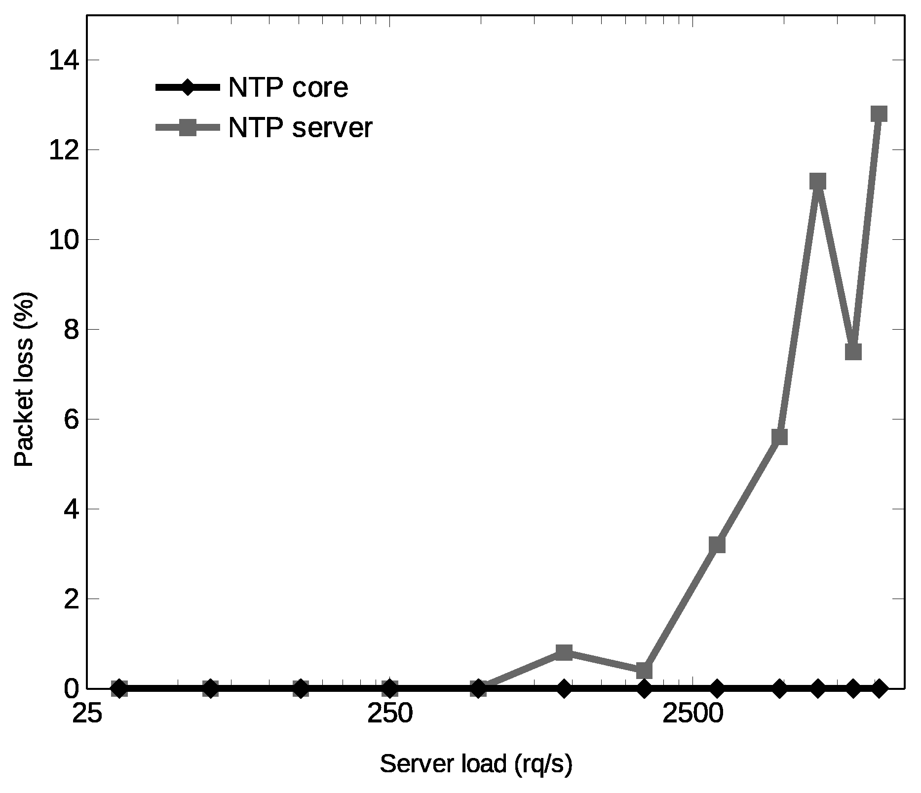
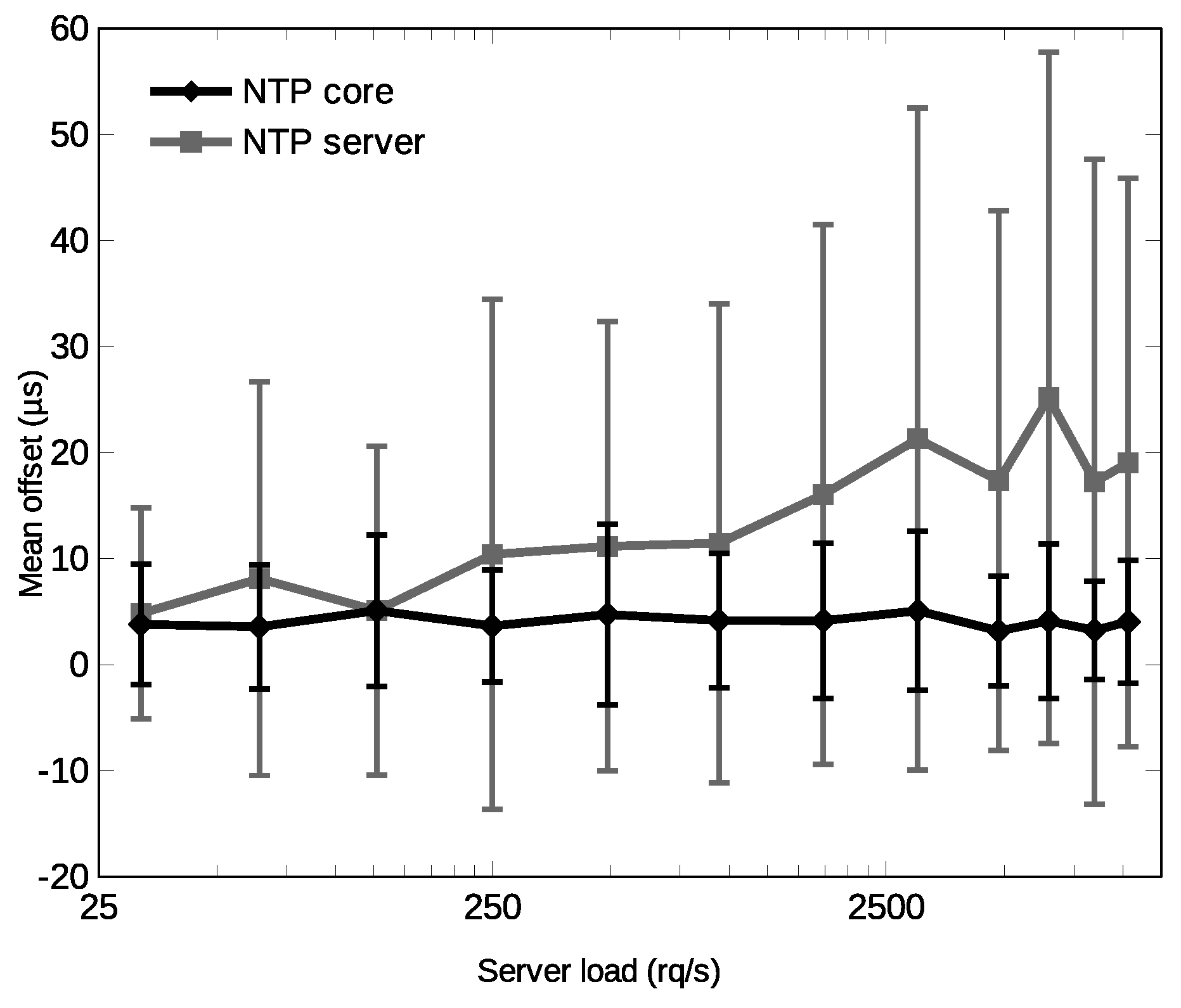
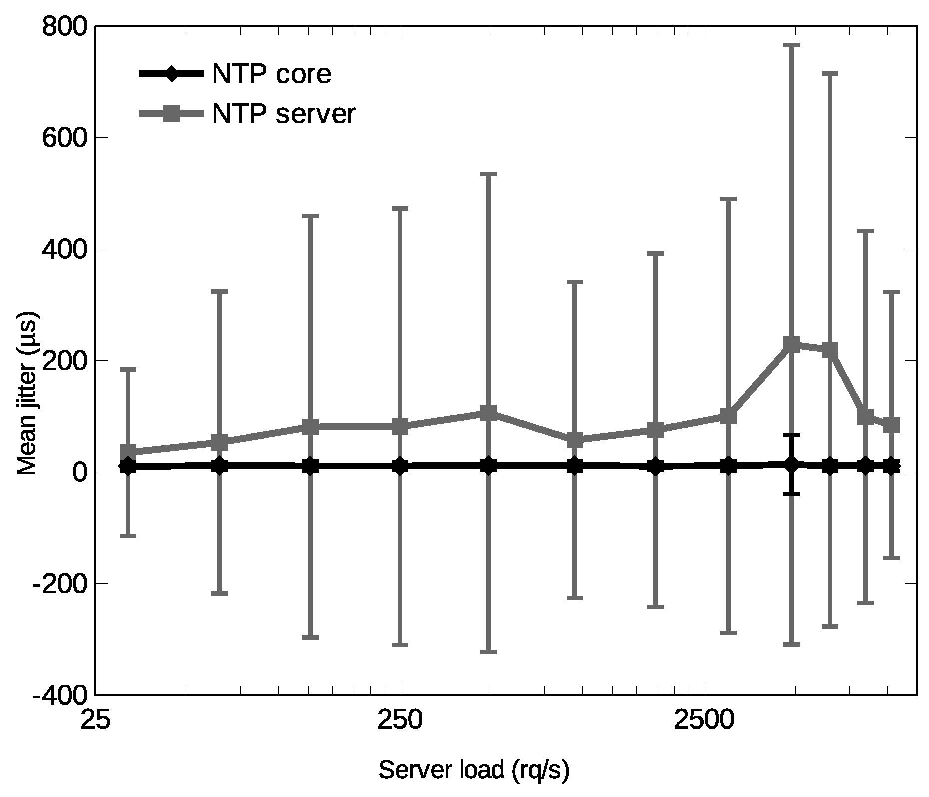
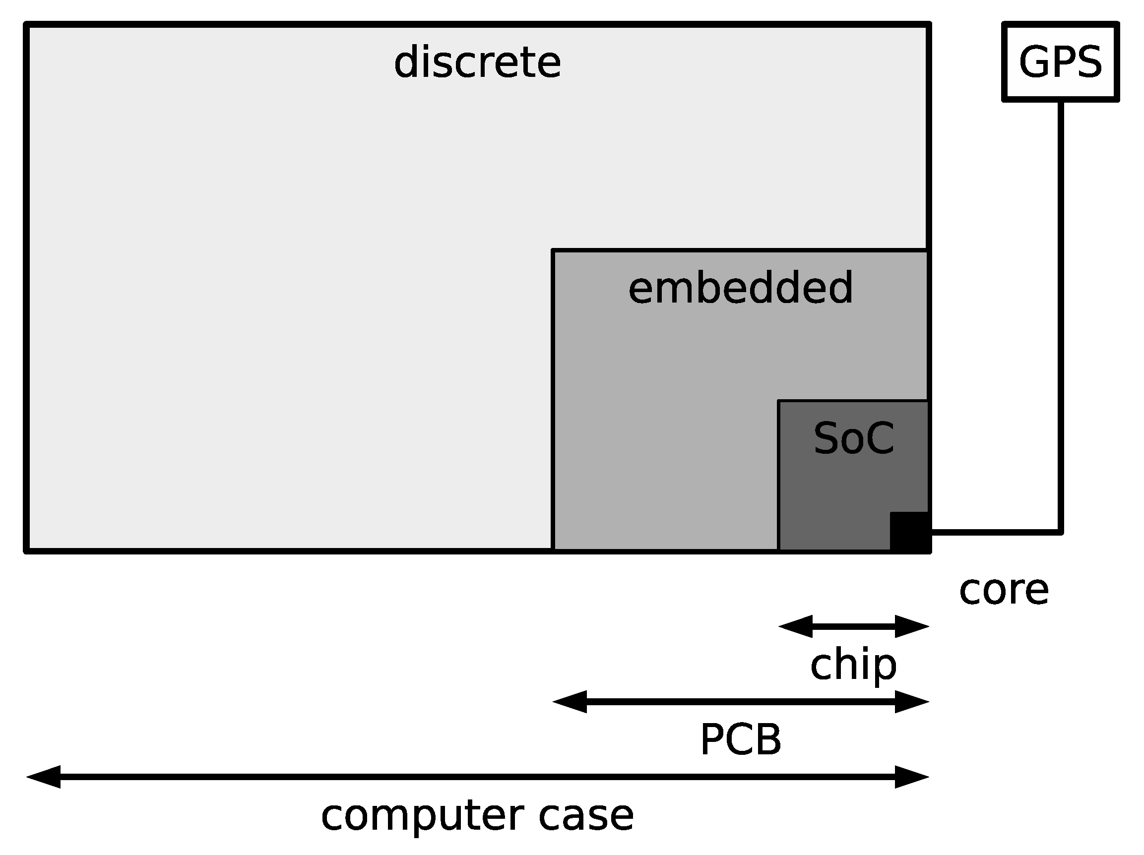
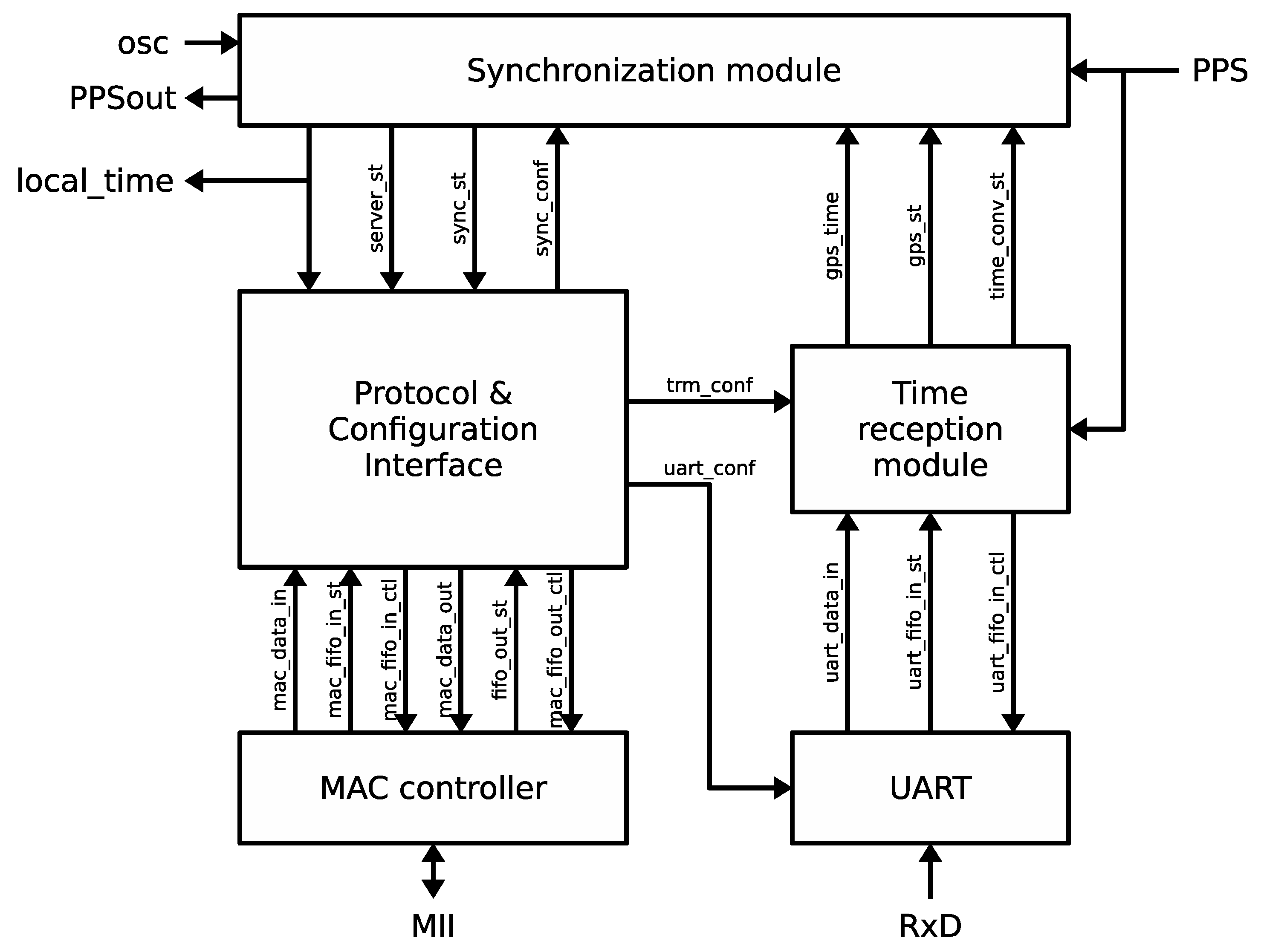
The synchronization module is the core of the timekeeping subsystem, in which the UART and the time reception modules are working as an interface to the GPS receiver. These modules are described in this section.

5.1. UART

The UART is used by the NTP server to receive time data from the GPS receiver through the popular electronic industries alliance (EIA) RS-232. RS-232 has been selected for its low-cost and wide availability. UART’s are standard modules easily available in embedded systems design libraries. In the present paper, a Xilinx’s intellectual property (IP) UART core has been used [34]. It is connected to an external RS-232 transceiver and includes both transmitter and receiver modules, although only the latter is needed in this case.
GPS receivers universally use the national marine electronics association specifications NMEA-0183 [35] to transmit data. The specification defines both the communication parameters and the format of the data. The UART uses a fixed data format of 8 data bits, no parity bit and one stop bit (8-N-1), according to the NMEA-0183 specification. Although this specification establishes a communication speed of 4800 bps, many GPS receivers in the market support higher baud rates to be able to transfer several frames in a single second. For this reason, the UART baud rate can be configured through the uart_conf bus coming from the P&CI (see Figure 5). A 4-bit code determines the baud rate according to Table 2.
As soon as the GPS receiver transmits new data to the UART, they are stored in its internal 16-byte first-in, first-out (FIFO) queue and made available to the time reception module, which controls the UART’s communications. The internal FIFOs are implemented using FPGAs logic blocks since their sizes are relatively small.

5.2. Time Reception Module

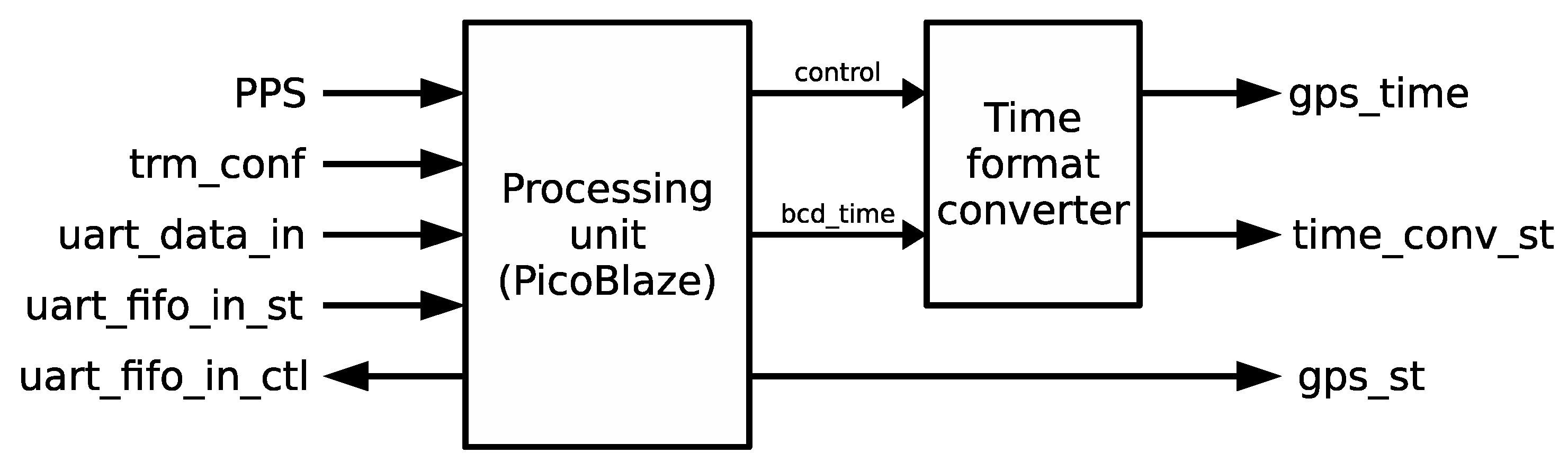
The mission of the time reception module is to collect information from the GPS receiver and transform it into time data and control signals that can be used by the synchronization module to maintain an accurate time in the local clock. The time reception module has two main blocks depicted in 
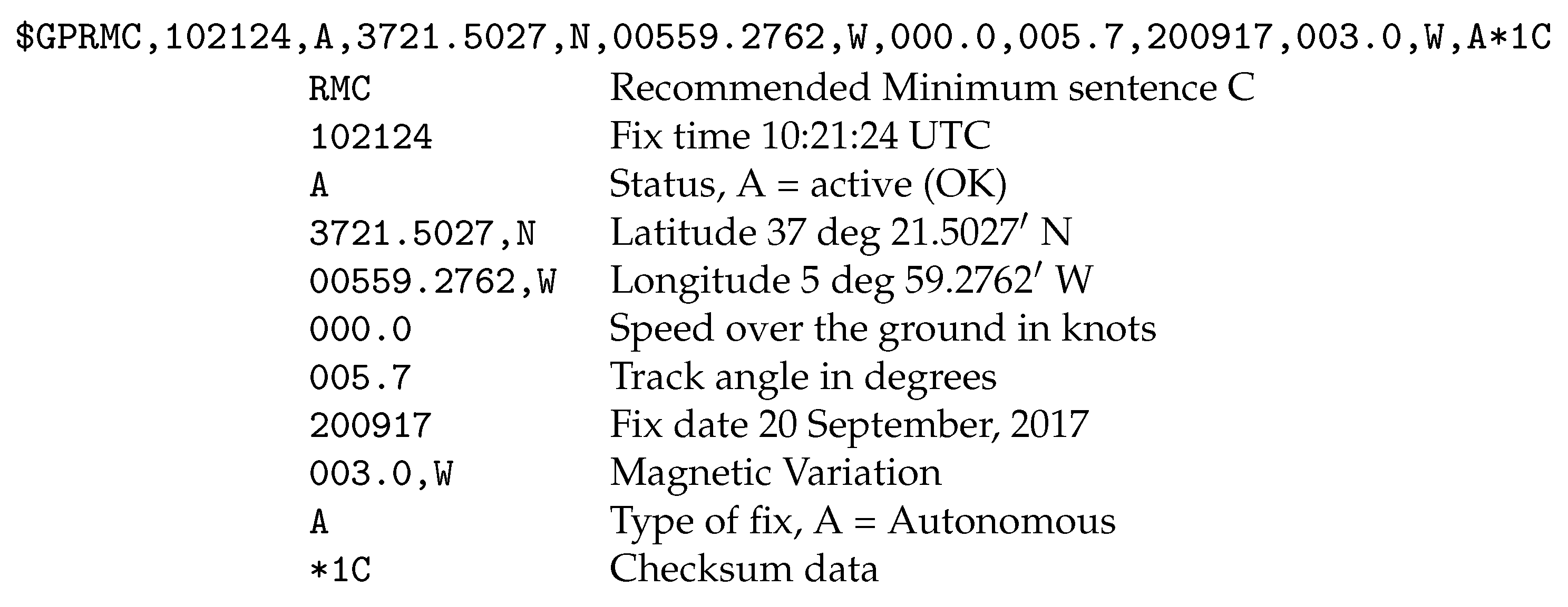
Figure 6: (i) Processing unit; and (ii) time format converter. The module operates as follows: the GPS receiver signals the starting of a new second with an active edge of the PPS signal. Following the edge, the GPS receiver emits a set of NMEA-0183 messages encoded in plain ASCII text. The message that is relevant for time synchronization applications is the recommended minimum sentence C (RMC), which covers date and time corresponding to the active edge of the PPS signal. The time reception module operation is triggered by the active edge of the PPS signal. Furthermore, a 1-bit configuration parameter included within the trm_conf bus indicates whether the expected active edge is a rising (1) or a falling (0) edge. Next, the time reception module starts receiving data from the UART, identifies the RMC frame and extracts time, GPS status and date information that is encoded in frame fields 1, 2 and 7, respectively. Figure 7 shows a sample RMC frame with decoded fields. After processing the RMC frame, date and time information is converted into NTP time format (seconds 00:00, 1 January 1900) and handed to the synchronization module through the 32-bit signal gps_time. Both the status of the GPS (active or not active) and the status of time conversion (correct or not correct) are also made available to the synchronization module through output signals gps_st and time_conv_st, respectively.
Most of the work in the time reception module is carried out by the processing unit, which is implemented by a Picoblaze 8-bit microcontroller [36] running a small program that is written in assembly language. Picoblaze is a tiny microcontroller and this programmatic approach greatly simplifies data extraction from the ASCII stream and control of the UART without having a significant impact on the overall resources utilization, as observed in Section 7.1. In addition, the use of a microcontroller here makes it much easier to deal with GPS communication debugging. Extracted date and time are stored in a set of binary-coded decimal (BCD) registers forming the bcd_time signal in day-month-year (DD-MM-YY) in the first case, and hour-minute-second (HH:MM:SS) format, in the second case.
The time format converter translates the BCD date and time data into NTP time format when signaled by the processing unit. This module has been implemented in HDL: a control unit manages a data path that processes the BCD registers sequentially and accumulates the total number of seconds represented by each register in the 32-bit output register gps_time.
The time reception module has been tested using KPicoSim [37] Picoblaze development environment and ISim logic-level simulator included within Xilinx ISE Design Suite [38].

5.3. Synchronization Module

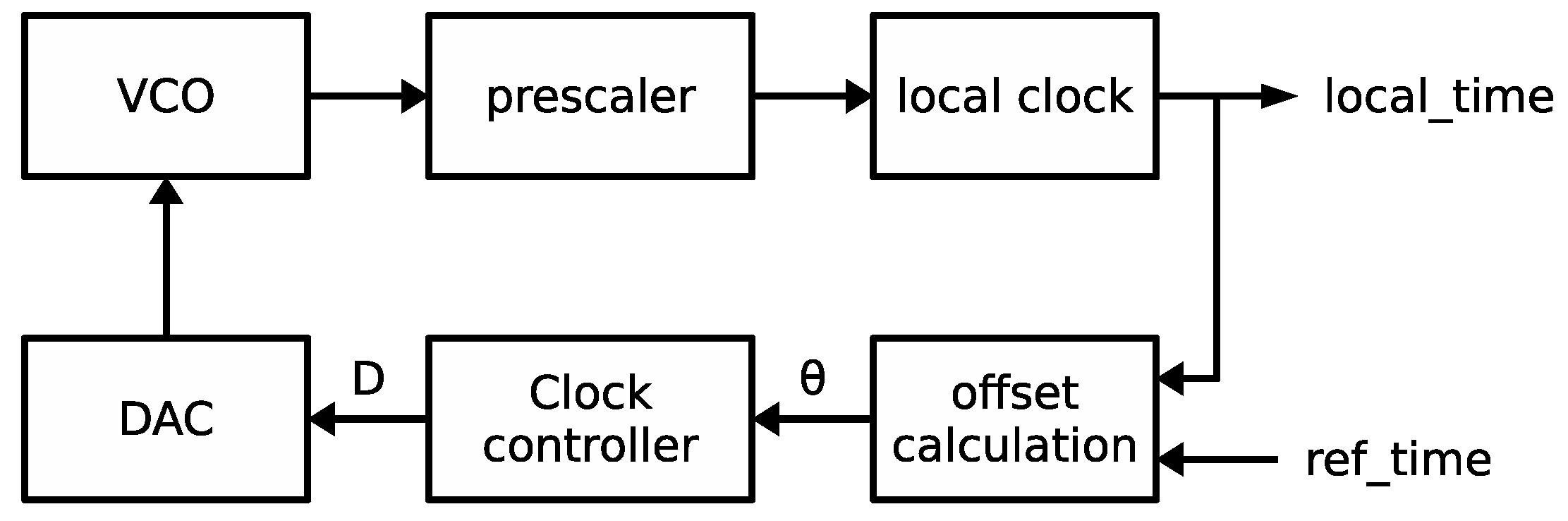
The task of the synchronization module is to maintain the local clock time as accurate and stable as possible by taking the GPS time as reference. This module is based on a clock model and a set of algorithms for continuously adjusting the local clock. It is the most complex one in the system after the P&CI. NTP implementations are typically based on the computer clock model introduced in [39] and shown in Figure 8. In this model, a voltage-controlled oscillator (VCO) generates a clock signal with a base frequency that a prescaler circuit turns into a proportional frequency better suited to drive the local clock. At each iteration of the control algorithm, the offset between local time and reference time ( θ ) is calculated. Thereafter, a clock controller uses a clock discipline algorithm to adjust the control voltage of the VCO through a digital-to-analog converter (DAC) circuit in order to maintain the local clock correctly synchronized with the reference.
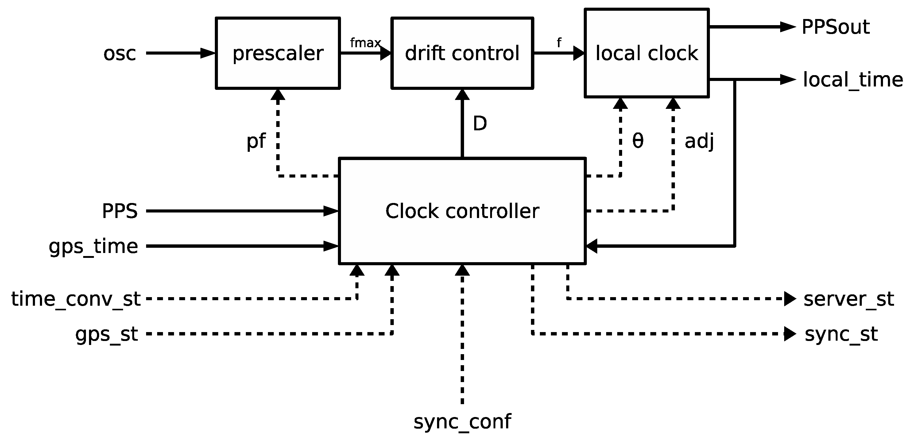
The synchronization module uses a different approach focused on the all-digital clock model introduced in [24] and adapted to the NTP server core, as Figure 9 shows. Compared to the traditional clock model, the most remarkable difference is that the VCO has been substituted by a completely digital drift control block, therefore eliminating the need of external components, like VCO and DAC. Solid lines in Figure 9 correspond to signals used by the synchronization module during a normal operation, when the local clock is synchronized with the reference clock and only slight modifications of the local clock frequencies are necessary to maintain the synchronization. Dashed lines are related to signals that are relevant during the initial configuration phase of the module or when the synchronization has been lost and the local clock needs to be re-adjusted.
The base frequency f o s c comes from a fixed-frequency clock signal o s c that is divided by the prescaler into a new frequency f m a x = f o s c / p f , where p f is an 8-bit prescaler factor included in the sync_conf configuration bus. This factor can be modified to accommodate a wide range of external oscillator frequencies in order to produce a f m a x that is close, but slightly higher, than the nominal frequency at which the local clock would run with no drift ( f n o m ). Afterwards, the drift control block selectively introduces a small time shift in f m a x by skipping a scattered fraction of the input cycles, given by input D. As a result, the average frequency at the output of the drift control block (the frequency applied to the local clock) can be adjusted.
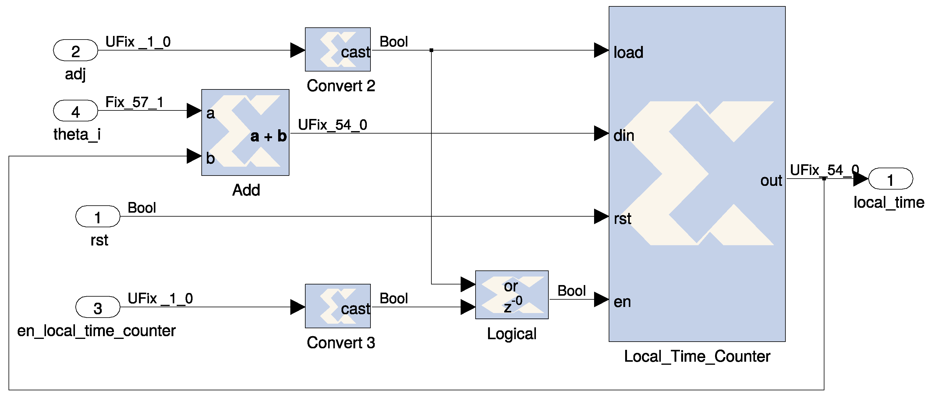
The local clock stores the time in NTP format using 32 bits for the integer part of the second and n bits for the fractional part. The resolution and tuning capabilities of the system are derived from n. The internal time resolution of the local clock is 2 n  s and the nominal operating frequency f n o m that would make the local clock run synchronized is f n o m = 2 n . The drift control unit is designed so that it can skip D cycles every 2 n cycles, consequently:
f = f m a x f m a x × D 2 n
but, since the prescaler is configured as f m a x f n o m , the previous equation can be approximated by:
f f m a x D .
In the current implementation, n = 22 , f n o m is approximately 4.19  MHz and time resolution is 238 ns, as can be seen in the local clock internal diagram in Figure 10. It means that the minimum frequency adjustment is about one quarter of the microhertz. This resolution is intended to provide local clock accuracy in the range of 1 μ s. Furthermore, a system clock of 50 MHz is used to drive o s c with a prescaler factor of 1 / 11 that yields a maximum frequency ( f m a x ) of 4.54  MHz. It means that the average frequency of the local clock can be adjusted in a range of ± 9 % with respect to the nominal clock frequency. Due to this range, small corrections can be performed to the local clock during normal operation.
It is along normal operation (solid lines in Figure 9) that the clock controller periodically compares the local time with the GPS time coming from the time reception module through the g p s _ t i m e signal and calculates the offset θ . Because the GPS time is only precisely known at the active edge of the PPS signal, this is taken as the trigger to run the adjustment process. At this point, the GPS time at g p s _ t i m e signal actually corresponds to the previous active edge of the PPS signal, since NMEA-0183 frames are only sent by the GPS unit after the active edge. Nevertheless, as the active edge occurs at the beginning of the second, the offset can be calculated right after identifying the edge as:
θ = ( g p s _ t i m e + 1 ) l o c a l _ t i m e .
A new value of the adjustment parameter D is calculated at every adjustment interval to keep the local clock tuned to GPS time. This adjustment process is controlled by the clock discipline algorithm specially designed for hardware implementation, as introduced in [24]. The algorithm tries to maintain the exactitude of the local clock, the stability of the clock frequency and a minimum drift of the local time when the GPS reference is not available for any reason. For that purpose, the clock discipline algorithm constantly computes the best value of D ( D n o m ), which would make the local clock run at the nominal frequency f n o m , and the additional correction to D, in order to make the local clock converge on the reference time in a smooth way. The actual implementation details of the algorithm are shown in
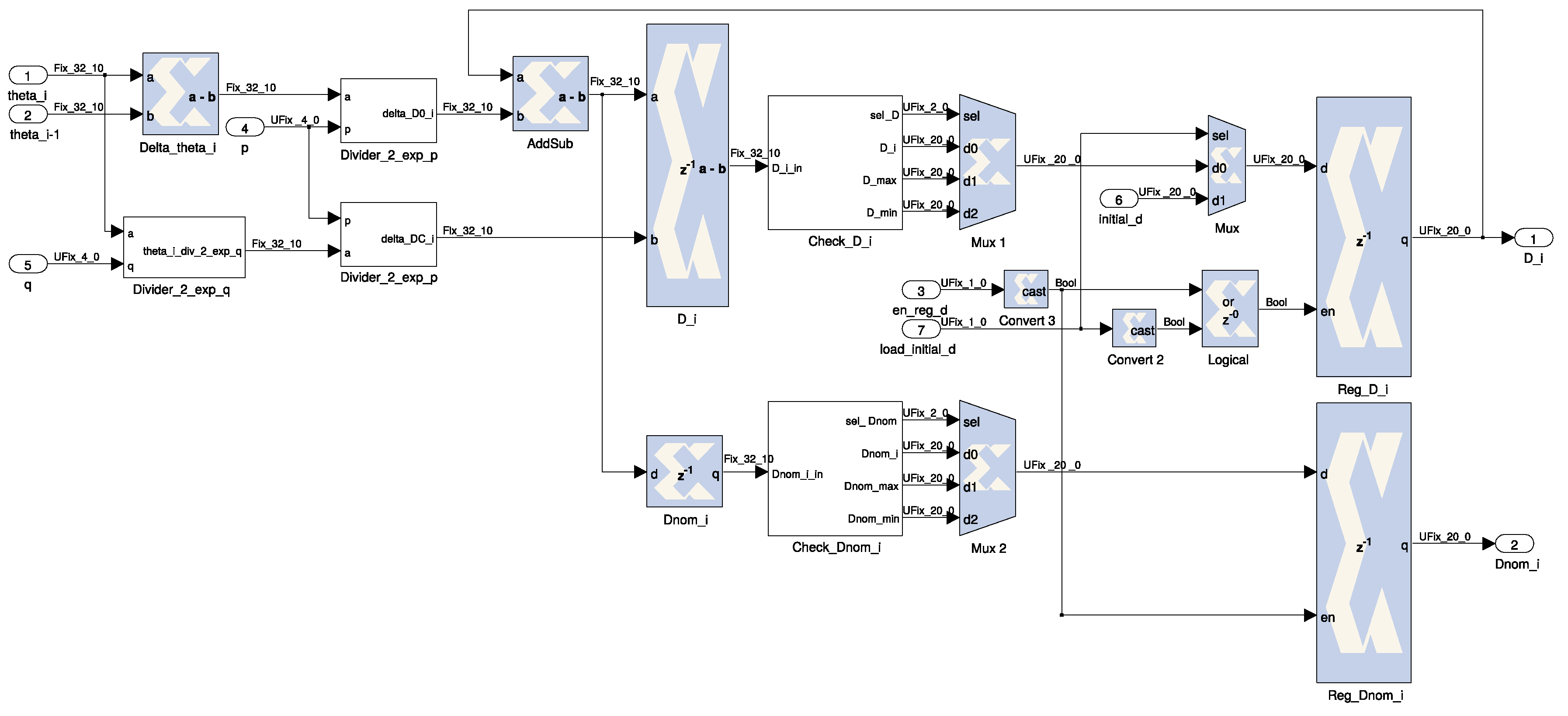
 Figure 11 where theta_i and theta_i-1 are the current and previous offset values, respectively; p and q are two convergence factors, which can be altered for testing and/or fine-tuning purposes; and D_i is the calculated correction. The module is implemented by using regular logic like shifters (power of 2 dividers), registers and simple arithmetic. Please refer to the work of Viejo et al. [24] for additional details.
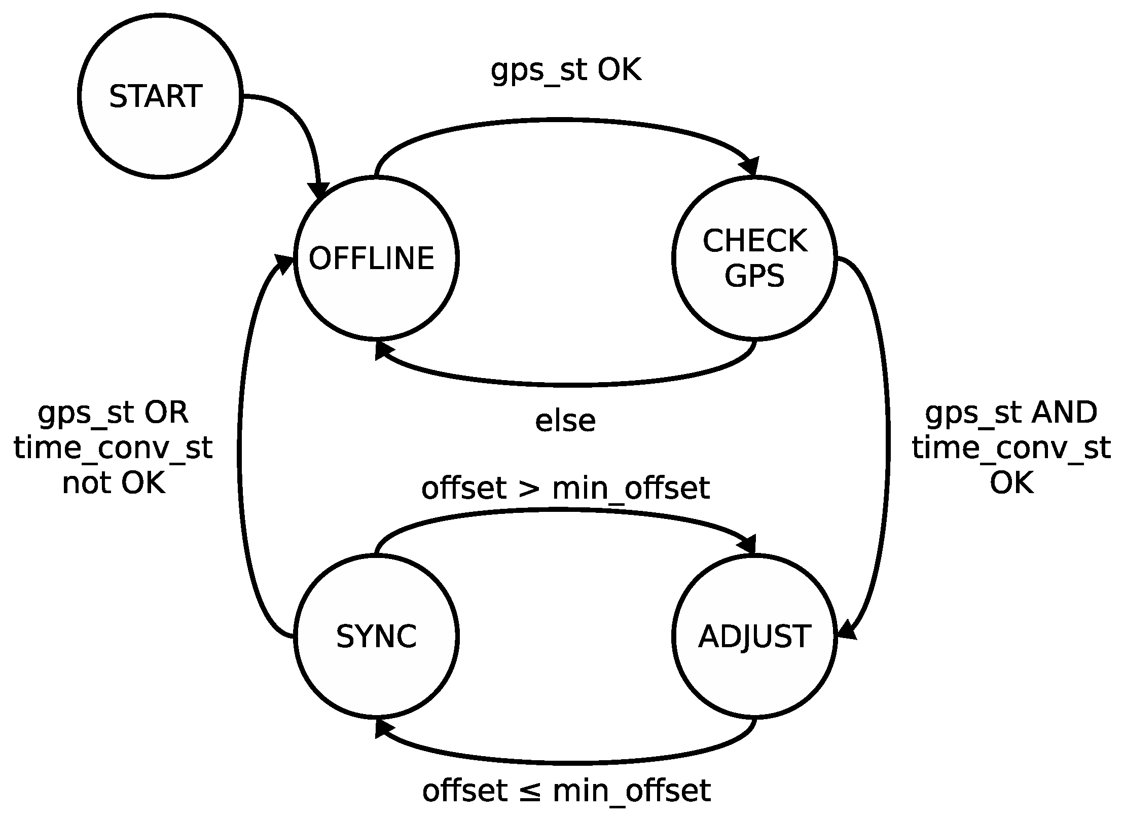
Furthermore, from the normal synchronized operation described in the previous paragraphs, the clock controller also handles the initial configuration and synchronization recovery by following the synchronization algorithm summarized in Figure 12. Upon system initialization, the controller is in START state and it is provided with the configuration for the synchronization module coming from the P&CI module through the sync_conf bus. This bus not only contains the information about the active edge of the PPS signal, the prescaler factor and two 4-bit convergence factors for the clock discipline algorithm, as previously mentioned, but also a 20-bit initial value of parameter D (see Figure 11).
Once configured, the controller moves to offline state. Afterwards, the following state transitions are triggered by the active edge of the PPS signal or by a watchdog signal set a few instants after the expected PPS edge, in case the GPS becomes unavailable. The GPS on-line state is checked through the gps_st signal coming from the time reception module. When the GPS is on-line, the system transitions to check GPS state, where the time conversion executed by the time reception module after the last active edge of the PPS signal is checked through the time_conv_st signal. If the conversion succeeds and the GPS receiver is still on-line, then there is a transition to adjust state, else the system returns to offline state.
Adjust state is intended to set the local clock to the reference time for the first time, once the system has been initialized, or when the local clock has drifted considerably from the reference clock after a long period of off-line operation. In this state, if the clock offset calculated as Equation (4) is within a minimum value min_offset, then the system is considered synchronized and moves to sync state. Otherwise, the clock controller activates the adj signal of the local clock causing it to add the offset to the local time, which sets the local time equal to the current GPS time (one second more than the previous GPS time in the gps_time signal). Since this hard adjustment is likely to be non-monotonic, it should be avoided in most cases by setting min_offset to the maximum offset value tolerated by the intended application, commonly in the range of a few seconds. Later, the system is synchronized and moves to sync state.
While in sync state, the system runs normally as described at the beginning of this subsection. If the offset overcomes min_offset, then the system moves back to adjust state and a hard adjustment of the local clock is forced. Nevertheless, this situation hardly ever happens in an already synchronized system and may reflect either a malfunction of the GPS receiver or a wrong operation of the clock discipline algorithm implemented by the clock controller. In case that either the GPS receiver becomes off-line or the time conversion does not work correctly, the system moves to offline state and waits for a correct GPS output to be available. While in this state, the clock discipline algorithm sets the drift control parameter to D n o m , in order to minimize the wandering of the local clock whenever the time reference is not available.
The clock controller also generates two state signals that are useful to build an NTP reply according to the NTP specification [5]. The sync_st indicates whether the synchronization module is currently synchronized or not with the time reference and can be used to determine the present stratum of the server. The server_st is a bundle of state signals including whether the local clock has been synchronized with the reference since startup, as well as the last time it happened. It also includes an estimation of the actual accuracy of the local clock.
As referred above, the current implementation uses 50 MHz global clock signal of the system to drive the reference clock signal of the synchronization module (osc). However, this signal is made externally available in case the stability of the system under a failure of the GPS needs to be improved by using a more accurate external reference, such as temperature compensated or oven-controlled crystal oscillator.
The synchronization algorithm in Figure 12 was been implemented using a finite state machine (FSM) coded in HDL. Data processing inside the clock controller includes extensive arithmetic operations for offset and control parameters calculations. Xilinx system generator for DSP has been used to model and implement the data processing part, which has been tested through Xilinx’s supported design flow based on MATLAB [40] and Simulink [41].

6. Communication Subsystem

The P&CI is the core of the communication subsystem and the most complicated module in the system as a whole. It is responsible for handling network communications and providing the rest of the modules in the system with the necessary configuration data. The P&CI implements the required functionality of the internet protocol (IP), UDP, NTP, BOOTP and address resolution protocol (ARP), using the MAC controller as the interface to lower-level communications. The P&CI needs to execute three tasks in parallel, associated to different protocols, which are referred to as services:
  • Configuration service (BOOTP): Initially IP and system configuration retrieval, and later configuration updates.
  • Time server service (NTP): Answers NTP request from NTP clients, the main task of the system.
  • Address resolution service (ARP): Answers ARP requests from other hosts in the local area network (LAN).
The P&CI uses the block architecture in Figure 13. Both design and operation of these blocks are detailed below in this section.

6.1. Ethernet MAC Controller

The Ethernet MAC controller implements the standard Ethernet functionality of the IEEE 802.3 specification [42], thus supplying the system with the data link layer of the open systems interconnection (OSI) model [43] and leaving upper layers in the protocol stack for the P&CI. The MAC controller connects to the external PHY through the MII. MAC controllers are standard modules in many embedded systems projects and there is a meaningful number of options available from hardware library vendors and from the embedded systems design community in general.
In regard to the system presented in this paper, the Ethernet MAC functionality is taken from the tri-mode Ethernet MAC module that is available in the OpenCores project [44]. It is implemented in Verilog code and the open-source nature of this module allows tailoring the design for this specific application. It has been necessary to slightly modify the original code with the aim of adapting the input/output signals to fit the global system architecture. The FIFO transmission and reception queues in the module have been optimized by means of available block RAM (BRAM) resources in the FPGA. In light of this, the transmission and reception latencies of the module have improved in order to achieve a more accurate timestamping of NTP packets and better synchronization precision, accordingly.
Although the MAC module supports operating up to 1 Gbps, it is limited to 100 Mbps in the current implementation in order to be able to operate with a 50 MHz system clock. However, 1 Gbps can be supported by using a system clock minimum frequency of 125 MHz.

6.2. Reception Block

The reception block monitors the input FIFO queue of the MAC controller and processes the incoming packets. Firstly, it determines whether the destination MAC address of the packet is that of the device or the broadcast address and, in this case, it reads the rest of the packet. Secondly, it identifies whether the packet corresponds to a service handled by the system, that is, a BOOTP reply, an NTP request or an ARP request. If the packet is none of these types then it is discarded, otherwise, the information in the packet is processed as follows:
  • If the incoming packet is an NTP request from a client then the MAC address and IP address of the client are both extracted from the packet together with the origin timestamp T 1 . They are delivered to the packet builder block through the packet_data bus, so that the appropriate reply can be built later.
  • If the incoming packet is an ARP request then the MAC address and IP address of the sender are both extracted and placed on the packet_data bus, so that the packet builder can store it with the aim to build the corresponding reply.
  • If the incoming packet is a BOOTP reply then it is processed to extract the IP configuration of the server (IP address, network mask and default router) and the filename string field of the BOOTP reply. All these pieces are made available to the configuration block through the conf_data bus.
The reception block has been implemented by an FSM coded in HDL. The FSM reads the bytes in the incoming packet and distributes the information in a set of registers which drive the data outputs of the block. Once the incoming packet is processed, the status of the reception block is updated and the P&CI control unit is signaled through the recept_st signal so that appropriate actions can be taken.

6.3. Configuration Block and Timers

The configuration block centralizes and stores the various bits of information required by the P&CI itself and by the other modules in the system. The parameters administered by the configuration block are shown in Table 3 together with the bus used to deliver each parameter to its destination. The parameters obtained by the BOOTP configuration process are called dynamic and are loaded at system startup. Nonetheless, they can be updated at run time by a new BOOTP request. The parameters that are hard-coded in the design’s programming file (bitstream) are called static and contain fixed values that cannot be altered after the FPGA chip has been programmed. The MAC address and the IP configuration parameters are made available to the packet builder in the pb_conf bus. Similarly, parameters for the UART, time reception and synchronization modules are transferred through their respective buses, as already described in previous sections.
The baud rate of the UART and the PPS active edge of the GPS receiver are dynamic parameters encoded in the text field filename of the BOOTP reply that are used by the reception block. The first character of the field represents the baud rate according to Table 2, whereas the second character is “0” for a falling PPS active edge and “1” for the opposite. This way of encoding some of the internal parameters of the NTP server makes it easy to alter their values by editing the BOOTP configuration file in the BOOTP server. Figure 14 displays a sample self-explicative configuration file for the internet systems consortium (ISC) DHCP/BOOTP server [45]. In the example, ntp-server-1 has been configured with an UART baud rate of 19,200 bps and a rising PPS active edge, whereas ntp-server-2 uses a baud rate of 9600 bps and a falling PPS active edge.
The P&CI uses a timer to control the sending of BOOTP requests. The timers block is configured with the system’s clock frequency in Hertz and a timeout number of seconds given by the BOOTP timeout parameter. Timers’ configuration goes in the t_conf bus. The timers block can be extended to support additional timers, with timeout outputs bundled in the t_out signal connected to the P&CI control unit (Figure 13).
The configuration block has been completely described in HDL by using a main FSM that manages the processing of data coming from the reception module and the distribution to the output registers. A secondary FSM is used to decode and check for possible errors in the filename field, as well as assign the resulting binary values to the trm_conf and uart_conf buses. Static parameters are internally stored in BRAM and can be directly modified in the bitstream file, without having to run the whole implementation process again, by using the Xilinx tool data2mem [46]. This tool is especially useful not only to change the server’s MAC address, which needs to be unique for every programmed chip, but also either for testing different configurations or for adapting the implemented design to a different master clock frequency. During the initialization of the block, the parameters stored in the BRAM are moved to conventional registers that drive the corresponding output signals.
The timers block has been designed by using regular counters from the Xilinx System Generator tool library.

6.4. Packet Builder, Packet RAM and Transmission Block

The packet builder is in charge of building the different types of outgoing packets the NTP server core needs to support: BOOTP requests, NTP replies, ARP requests and ARP replies. The packet builder is supported by a packet RAM that acts as a workspace for the packet builder. It holds a template of an Ethernet frame for every packet type needed. The templates are located at known addresses within the packet RAM, conforming to the memory map in Table 4. When the control unit requests building a particular type of packet through the pb_ctl signal, the packet builder gathers the needed information from its input signals or internal registers, and completes the packet fields in the appropriate template within the packet RAM. If necessary, checksums are also calculated and stored, such as in the transmission of UDP packets. Once the needed packet is built, the control unit is informed through the status signals in the pb_st bus.
The packet builder is also responsible both for collecting the origin timestamp ( T 1 ) of incoming NTP requests processed by the reception block and for issuing the corresponding receive timestamp ( T 2 ) by using the local_time signal from the synchronization module. These timestamps are stored in the packet builder internal registers to be used to build the NTP reply to the last NTP request.
The packet building process is similar for all the types of packets. BOOTP request packets are directed to the local broadcast address carrying the MAC address of the server with it. NTP reply packets are built with the information of the corresponding request previously stored (origin and receive timestamps) together with the local time and local clock status coming from the synchronization module. The transmit timestamp ( T 3 ) is obtained from the local_time signal. The stratum of the server is set in terms of the sync_st signal. If the signal value is 0, then the GPS receiver time is not valid or the synchronization with the GPS is not correct. In this case, the stratum of the server is set to 0, otherwise it is set to 1, since it is a primary server connected to a GPS reference. The server_st bus is used to fill in the precision field of the NTP reply. Other NTP fields are completed following the NTP specification [5].
In a similar way, ARP replies use the previously stored sender’s MAC and IP addresses and complete the data with the server’s MAC and IP addresses and other information required by the ARP protocol [47]. The packet builder and RAM also have provisions to build ARP request packets, but this functionality is not used in the current version of the server, since the only communication initiated at the server are BOOTP requests that are issued to the LAN’s broadcast address.
Once an outgoing packet has been built, the control unit activates the transmission block and indicates the type of packet to be transmitted by means of the trans_ctl bus. The transmission block then reads the packet previously produced in the packet RAM from the address corresponding to the type of transmission and it passes the data to the output FIFO queue of the MAC controller. The transmission block also detects any condition of the MAC controller that would require a new packet to be built, e.g., a collision in the MAC level that would need to rebuild the NTP reply with a refreshed transmit timestamp.
Both the packet building process and the data transmission to the MAC are controlled by FSMs described in HDL. The packet RAM is built out of BRAM memory available in the FPGA chip. BRAM has the advantage of being a synchronous memory, therefore contributing to have a fixed transmission delay time, which is important for the stability of the NTP time synchronization.

6.5. P&CI Control Unit and Operation

The role of the control unit is to coordinate the operation of the rest of the blocks that form the P&CI module. This task is relatively simple because, as stated in the previous sections, all communication and configuration tasks, including NTP timestamping, are completely handled by the blocks in the module in a very independent way, only requiring some coordination. The time server service can be given as an example: when an NTP request packet arrives to the reception module, the packet is fully processed before the control unit is signaled. If the reception has been correct then the control unit only needs to activate the packet builder as well as the transmission block in turn, and the NTP reply is automatically crafted and sent out. The algorithm to control this service can be described by the pseudo-code in Figure 15, which can be easily implemented by an FSM. Analogous simple algorithms are used to coordinate the configuration service and the address resolution service that have to do with BOOTP packets in the first case and ARP packets in the second case.
In practice, the main challenge for the P&CI control unit is to run the three services in parallel in a coordinated way, avoiding any conflicts among them. For instance, the configuration service may need to issue a BOOTP request, while the time server service is replying to an NTP request. To solve this problem, the P&CI control unit uses separate FSMs to control each service. The access of these services to the underlying blocks is controlled by a service arbiter that only grants access to one service at a time. Figure 16 shows the overall architecture of the arbitration system. Each service block is connected to the status signals of the processing blocks in the module and can actuate on their control signals as well, but only when access has been granted by the service arbiter.
The handshake mechanism between services and the arbiter is very simple: if Service i wants to access the processing blocks, then it will assert the request signal rq_i and will wait for signal gt_i to be asserted by the arbiter granting the requested access. When the service block finishes its tasks, it de-asserts the request signal and the arbiter may grant access to another service. Collision of services (two or more services requesting access at the same time) during the normal operation of the system is very unlikely to happen, since NTP and ARP requests will normally be replied intermediately and the BOOTP service only needs to be run once every several seconds. Therefore, the arbiter follows a simple fixed priority algorithm with the highest priority given to the time server service, as it is the most time-critical service, and the lowest priority assigned to the BOOTP service.
Service blocks are expected to remain inactive until triggered by the event’s triggering signal trig_i. Triggering signals for the time server and ARP services come from the bits of the recept_st bus that indicate the arrival of an NTP or ARP request, respectively. Hence, these services act as server services because they are triggered by a request packet coming from the outside. On the contrary, the triggering signal for the BOOTP service comes from the timers block output bus t_out, causing the BOOTP service to be activated every time the BOOTP timer expires. As mentioned in Section 6.3, the BOOTP timer can be configured through the static parameter BOOTP timeout, with reasonable values ranging from one to several minutes. The BOOTP service plays the role of a client service since it is initiated within the P&CI itself.
It is worth mentioning that the proposed service architecture allows for the easy inclusion of additional client and/or server services in future revisions of the systems. An additional server service might provide time synchronization utilizing a different protocol, otherwise a new client service could broadcast state information. Obviously, adding additional services is likely to require additional functionality in the P&CI or the whole system.
All services together with the arbiter have been implemented in HDL through a standard FSM description technique. Furthermore, they have been validated by simulation in the Xilinx’s design framework.

7. Results and Discussion

To validate the proposed design and to estimate its performance, different aspects of the system have been evaluated: (i) Resources used by the implementation; (ii) Accuracy of the NTP core’s local clock with respect to time reference; (iii) Client-side precision measured by a standard NTP client; And (iv) performance of the server core operating under different load conditions. All accuracy and performance tests have also been carried out, side-by-side on a state-of-the-art high-performance NTP server: a LANTIME M600 from Meinberg [48]. The results are detailed in the following subsections.

7.1. Implementation Results

The NTP server core has been implemented on a XC3S500E chip: a low-range, now obsoleted, Xilinx FPGA device, with a master clock working at 50 MHz. The use of an old device helps to highlight the efficiency of the design and has also been useful to track the improvements with respect to the earlier designs developed by the authors in the same platform. Porting to newer chips and even a different FPGA vendor is simple and is planned as future work.
Table 5 summarizes the implementation results. The NTP core uses less than 50% of the chip’s resources, except for the number of slices, which is higher. Table 6 displays the number and percentage of hardware resources per module. Slices, flip-flops, Look-Up Tables (LUTs) and BRAM are shown separately. As expected, the P&CI uses more resources than the time reception module (TR mod. in Table 6) and the synchronization module (Sync. mod. in Table 6). The share of the MAC controller is also important while the impact of the UART is negligible. Less than 1% of the available slices and LUTs are consumed by miscellaneous logic (Misc. in the figure) including glue logic, start-up circuitry, as well as top-level routing and interconnections. Considering that the device is a low-range FPGA chip, it can be stated that the hardware footprint is reasonably low and that the overall resources occupation can easily go below 10% in any mid-range state-of-the-art FPGA chip.

7.2. Synchronization Accuracy to Time Reference

To measure the accuracy of the timekeeping subsystem, the PPS signal generated by the NTP core is compared to the PPS signal generated by a GPS receiver. The PPS of the LANTIME M600 high-performance NTP server (NTP server in the following) is also included as a reference. The measurement procedure takes place as follows: the NTP core and NTP server are run until synchronization is established and the offset value with respect to the GPS PPS signal is stable. Then, 1000 consecutive offset values are measured at the active edge of the GPS receiver’s PPS signal for both systems using a digital oscilloscope, which automatically computes the mean and standard deviation (SD) of the measurements (see Figure 17). As the results may vary depending on the state of the GPS constellation, the process is repeated four times at different times of the day and results are averaged (see Table 7).
Although the average measured offset of the NTP core is better than the NTP server’s ( 37 ns vs. 115 ns), it gives a larger dispersion represented by the SD (223 ns vs. 37 ns), which is of the same order as that of the maximum internal built-in resolution of the local clock (238 ns), as discussed in Section 5.3 above. It can be inferred that the techniques and timekeeping algorithms used in the synchronization module are performing extremely well, being only limited by the time resolution of the local clock. As a result, the NTP core’s local clock can easily maintain an accuracy below the microsecond, in the same range as the high-performance NTP server.

7.3. Client-Side Accuracy

The setup in Figure 18 has been used with the aim of measuring the achievable precision of a standard NTP client connected to the NTP core, as well as to compare it with a high-performance NTP server. A standard NTP software client version 4.2.6 [49] running in a desktop computer is synchronized with the high-performance NTP server and the NTP server core. Both are connected to the same LAN switch as the testing software client. The traffic generator in the picture is used to obtain additional results detailed below.
When synchronized with a server, the NTP client will continuously calculate the delay, offset and jitter associated to the server, as introduced in Section 3. These parameters, especially the offset and jitter, are good estimators to compare different servers performance in terms of the client’s perspective.
An equal procedure has been developed to test both servers: the NTP client is set to use a standard 64 s polling interval and delay, offset and jitter values are read every hour for nine hours by the standard NTP query program (ntpq). Table 8 shows the obtained results. After four hours, the values calculated by the client have stabilized (NTP clients are very conservative and they synchronize very slowly), and mean and SD statistics have been calculated through the values registered from 4 h to 9 h. These statistics are shown in Table 9. The delay of the NTP core is about half of the NTP server ( 97.8 μ s vs. 191 μ s), that is to say, keeping other conditions the same, the packet processing of the NTP core is faster than that of the NTP server, as expected from a hardware implementation. Although a faster response does not imply better accuracy, the smaller dispersion of the delay represented by the SD highlights the fact that NTP core responses happen in a more predictable way.
Offset and jitter values represent accuracy and stability of the server conforming to the client’s point of view. Figure 19 depicts these values with error bars representing a 95% confidence interval ( 1.96 × S D ). Offset confidence intervals are very similar for both, the NTP server and the NTP core, while the jitter interval of the core is much more narrow than that of the NTP server. It means that the client obtains similar accuracy when synchronized with either server in the band of ± 10 μ s, as expected in a software client [17]. However, the offset is more stable in the short term, when the client is synchronized with the NTP core, as the lower jitter highlights. Then, it can be concluded that accuracy and stability of the NTP core, as perceived by a standard NTP client, is at least comparable to that of a high-performance NTP server. The offset value is also in agreement with case 3 mentioned in [20] where hardware-assisted PTP client and server are connected through a regular switch and the client-server offset is measured with an oscilloscope giving an offset of 3.7 μ s. Since the measurements of the NTP core are obtained by a less accurate software-only NTP client, it can be said that the accuracy of the core is also comparable to previous SoC approaches when using standard network equipment.

7.4. Performance under Load

A key performance figure in an NTP server is the amount of NTP traffic that it can manage before NTP request packets start being missed and then, synchronization accuracy is affected. The response of the high-performance NTP server and the NTP core have been analyzed for different NTP network loads, ranging from 32 to 10,000 NTP requests per second (rq/s), which is the maximum load most manufacturers report for their NTP server products [8,9,10]. At a typical poll interval of 64 s, it is equivalent to serving more than half a million NTP clients.
The test scenario is the same as the one shown in Figure 18, although this time the NTP traffic generator is enabled. The generator uses the tcpreplay tool [50] to inject NTP network traffic in the LAN at a controlled data rate. It should be noticed that the LAN bandwidth used at the maximum NTP load tested is below 20 Mbps and it is far from the full-duplex 200 Mbps bandwidth of the standard switched 100 Mbps Ethernet LAN used in the setup. Furthermore, this time the poll interval in the client is set to 16 s in order to speed-up the data acquisition process. Both packet loss and load impact on servers accuracy, have been analyzed.

7.4.1. Packet Loss

Figure 20 summarizes the percentage of missed NTP responses (requests without an answer from the server) as a consequence of an increasing NTP network load. For every server load tested, the count of lost NTP packets is collected from the ntpq program, after making 750 requests in a time span of 200 min. The high-performance NTP server starts missing some NTP requests at about 1000 rq/s load. At 3000 rq/s, the percentage of lost requests increases sensibly to 3%, reaching a maximum around 12% for 6000 rq/s or more, up to the maximum tested load of 10,000 rq/s. In contrast, no packet loss has been registered in the NTP core at any of the tested server load conditions.

7.4.2. Load Impact on Server Accuracy

Equally as done in Section 7.3, 100 consecutive samples of delay, offset and jitter values have been obtained at one-minute intervals using the ntpq program. In addition, mean values and SDs for each parameter have been calculated. The process has been repeated for different NTP loading conditions and results are shown in Figure 21, Figure 22 and Figure 23. Each graph includes error bars indicating 95% confidence intervals. The synchronization parameters registered by the client when synchronized to the high-performance NTP server degrade as the server is under a higher load. Delay becomes less predictable, as Figure 21 represents, and the offset value increases from about 5 μ s, for very light load, to about 20 μ s, for a server load of 3000 rq/s or higher (Figure 22). The fact that the offset confidence interval spreads from about 20 μ s to more than 60 μ s as the load increases is even more noticeable. A similar behavior is observed in the jitter estimated by the client when synchronized with the high-performance NTP server. However, the most remarkable point is that the NTP core yields better results than the high-performance server in all parameters and tested conditions, and it is not significantly affected by the load in the tested range. In particular, the offset is always around ± 10 μ s range and the jitter is mostly between 5 μ s to 15 μ s interval (not appreciated in Figure 23).
The authors assume that the ability of the NTP core to provide clients with similar accuracy regardless of the loading conditions is a direct consequence of decoupling between the timekeeping subsystem and the communication subsystem present in the core’s architecture, as commented in Section 4.

8. Conclusions

This paper has presented the complete design and implementation of an all-hardware NTP server core for FPGA. By using a carefully designed modular architecture, hardware-optimized timekeeping algorithms and a range of digital design techniques, the server core is able to achieve similar accuracy and performance of state-of-the-art high-performance NTP server equipment. It can also serve hundreds of thousands of NTP clients without any sensible accuracy degradation up to a minimum of 10,000 NTP requests per second, outperforming a reference industrial-grade time server.
The core utilizes a common GPS receiver as time reference and it does not require an external voltage-controlled oscillator to operate. The NTP server core has a small footprint and easily fits in a low-range logic-only FPGA chip, scaling down from previous SoC-level time synchronization systems found in the literature. Consequently, it offers a valuable time server solution for a wide range of emerging highly distributed network applications and the IoT.

Author Contributions

Conceptualization, J.J.-C. and M.J.B.; methodology, J.V., J.J.-C. and M.J.B.; software, J.V. and E.O.; validation, J.V., E.O., P.R.-d.-C., D.G. and G.C.; formal analysis, J.V. and J.J.-C.; investigation, J.J.-C., M.J.B. and J.V.; resources, E.O. and P.R.-d.-C.; data curation, J.V. and E.O.; writing—original draft preparation, J.V. and J.J.-C.; writing—review and editing, J.V., J.J.-C., M.J.B., P.R.-d.-C., E.O., D.G. and G.C.; visualization, J.J.-C. and J.V.; supervision, J.J.-C. and M.J.B.; project administration, J.J.-C. and P.R.-d.-C.; and funding acquisition, J.J.-C. and P.R.-d.-C.

Funding

This work was partially supported by the Ministerio de Industria y Competitividad of Spain under project TIN2017-89951-P (BootTimeIoT) and by the European Regional Development Fund (ERDF).

Acknowledgments

This work was partially supported by the Ministerio de Industria y Competitividad of Spain under project TIN2017-89951-P (BootTimeIoT) and by the European Regional Development Fund (ERDF).

Conflicts of Interest

The authors declare no conflict of interest. The funders had no role in the design of the study; in the collection, analyses, or interpretation of data; in the writing of the manuscript, or in the decision to publish the results.

References

  1. Flammini, A.; Ferrari, P. Clock Synchronization of Distributed, Real-Time, Industrial Data Acquisition Systems. In Data Acquisition; Vadursi, M., Ed.; IntechOpen: London, UK, 2010; Chapter 3; pp. 41–62. [Google Scholar] [CrossRef]
  2. Mazur, D.C.; Entzminger, R.A.; Kay, J.A.; Morell, P.A. Time Synchronization Mechanisms for the Industrial Marketplace. IEEE Trans. Ind. Appl. 2017, 53, 39–46. [Google Scholar] [CrossRef]
  3. Stankovic, J.A. Research Directions for the Internet of Things. IEEE Internet Things J. 2014, 1, 3–9. [Google Scholar] [CrossRef]
  4. Lévesque, M.; Tipper, D. A Survey of Clock Synchronization Over Packet-Switched Networks. IEEE Commun. Surv. Tuts. 2016, 18, 2926–2947. [Google Scholar] [CrossRef]
  5. Mills, D.L.; Martin, J.; Burbank, J.; Kasch, W. Network Time Protocol Version 4: Protocol and Algorithms Specification, RFC 5905 (Standards Track). Available online: https://www.ietf.org/rfc/rfc5905.txt (accessed on 25 March 2019).
  6. IEEE Standard for a Precision Clock Synchronization Protocol for Networked Measurement and Control Systems. Available online: https://standards.ieee.org/standard/1588-2008.html (accessed on 25 March 2019).
  7. Meinberg Funkuhren GmbH & Co. KG Home Page. Available online: https://www.meinbergglobal.com/ (accessed on 25 March 2019).
  8. Microsemi Home Page. Available online: https://www.microsemi.com/ (accessed on 25 March 2019).
  9. Galsys Home Page. Available online: https://www.galsys.co.uk/ (accessed on 25 March 2019).
  10. EndRun Technologies Home Page. Available online: http://www.endruntechnologies.com/ (accessed on 25 March 2019).
  11. GPS: The Global Positioning System. Available online: https://www.gps.gov/ (accessed on 25 March 2019).
  12. Alioto, M.; Sánchez-Sinencio, E.; Sangiovanni-Vincentelli, A. Guest Editorial Special Issue on Circuits and Systems for the Internet of Things–From Sensing to Sensemaking. IEEE Trans. Circuits Syst. I 2017, 64, 2221–2225. [Google Scholar] [CrossRef]
  13. Uesugi, Y.; Nonaka, T.; Sugiyama, S.; Hase, T. SNTP server and client system for home use. In Proceedings of the 13th IEEE International Symposium on Consumer Electronics (ISCE 2009), Kyoto, Japan, 25–28 May 2009; pp. 981–983. [Google Scholar] [CrossRef]
  14. Refan, M.H.; Valizadeh, H. Computer Network Time Synchronization using a Low Cost GPS Engine. Iran. J. Electr. Electron. Eng. 2012, 8, 206–216. [Google Scholar]
  15. Hwang, S.Y.; Yu, D.H.; Li, K.J. Embedded System Design for Network Time Synchronization. In Embedded and Ubiquitous Computing; Yang, L.T., Guo, M., Gao, G.R., Jha, N.K., Eds.; Springer: Berlin, Germany, 2004; pp. 96–106. [Google Scholar] [CrossRef]
  16. Chao, C.C.; Huang, S.P.; Hung, H.L. Embedded System on NTP. In Proceedings of the 4th International Conference on Computer Sciences and Convergence Information Technology (ICCIT 2009), Seoul, Korea, 24–26 November 2009; pp. 852–857. [Google Scholar] [CrossRef]
  17. Ferrari, P.; Flammini, A.; Rinaldi, S.; Bondavalli, A.; Brancati, F. Experimental Characterization of Uncertainty Sources in a Software-Only Synchronization System. IEEE Trans. Instrum. Meas. 2012, 61, 1512–1521. [Google Scholar] [CrossRef]
  18. Son, S.C.; Kim, N.W.; Lee, B.T.; Cho, C.H.; Chong, J.W. A time synchronization technique for coap-based home automation systems. IEEE Trans. Consum. Electron. 2016, 62, 10–16. [Google Scholar] [CrossRef]
  19. Kuwano, S.; Yamada, Y.; Hisadome, K.; Teshima, M. Hardware implemented network time protocol (HwNTP) based synchronization for digitized radio over fiber systems. IEICE Commun. Express 2012, 1, 4–9. [Google Scholar] [CrossRef]
  20. Moreira, N.; Lázaro, J.; Bidarte, U.; Jimenez, J.; Astarloa, A. On the Utilization of System-on-Chip Platforms to Achieve Nanosecond Synchronization Accuracies in Substation Automation Systems. IEEE Trans. Smart Grid 2017, 8, 1932–1942. [Google Scholar] [CrossRef]
  21. Jimenez-Lopez, M.; Gutierrez-Rivas, J.L.; Diaz, J.; Lopez-Marin, E.; Rodriguez, R. WR-ZEN: Ultra-accurate synchronization SoC based on Zynq technology. In Proceedings of the 30th European Frequency and Time Forum (EFTF 2016), York, UK, 4–7 April 2016; pp. 1–4. [Google Scholar] [CrossRef]
  22. Viejo, J.; Juan, J.; Bellido, M.J.; Ostua, E.; Millan, A.; Ruiz-de Clavijo, P.; Muñoz, A.; Guerrero, D. Design and implementation of a SNTP client on FPGA. In Proceedings of the 2008 IEEE International Symposium on Industrial Electronics (ISIE 2008), Cambridge, UK, 30 June–2 July 2008; pp. 1971–1975. [Google Scholar] [CrossRef]
  23. Viejo, J.; Juan, J.; Ostua, E.; Bellido, M.J.; Millan, A.; Muñoz, A.; Villar, J.I. Accurate and compact implementation of a hardware SNTP Client. In Proceedings of the 15th Iberchip Workshop (IWS 2009), Buenos Aires, Argentina, 25–27 March 2009; pp. 504–509. [Google Scholar]
  24. Viejo, J.; Juan, J.; Bellido, M.J.; Millan, A.; Ruiz-de Clavijo, P. Fast-Convergence Microsecond-Accurate Clock Discipline Algorithm for Hardware Implementation. IEEE Trans. Instrum. Meas. 2011, 60, 3961–3963. [Google Scholar] [CrossRef]
  25. Juan, J.; Viejo, J.; Bellido, M.J. Network Time Synchronization: A Full Hardware Approach. In Integrated Circuit and System Design. Power and Timing Modeling, Optimization and Simulation; Ayala, J.L., Shang, D., Yakovlev, A., Eds.; Springer: Berlin, Germany, 2013; Volume 7606, pp. 225–234. [Google Scholar]
  26. Daniluk, G.; Wlostowski, T. White Rabbit: Sub-Nanosecond Synchronization for Embedded Systems. In Proceedings of the 43rd Annual Precise Time and Time Interval Systems and Applications (PTTI 2011), Long Beach, CA, USA, 14–17 November 2011; pp. 45–60. [Google Scholar]
  27. Mills, D.L. Computer Network Time Synchronization: The Network Time Protocol, 1st ed.; CRC Press, Inc.: Boca Raton, FL, USA, 2006. [Google Scholar]
  28. Exel, R.; Bigler, T.; Sauter, T. Asymmetry Mitigation in IEEE 802.3 Ethernet for High-Accuracy Clock Synchronization. IEEE Trans. Instrum. Meas. 2014, 63, 729–736. [Google Scholar] [CrossRef]
  29. Holmeide, Ø.; Skeie, T. Synchronised: Switching. IET Comput. Control Eng. 2006, 17, 42–47. [Google Scholar] [CrossRef]
  30. Mills, D.L. Simple Network Time Protocol (SNTP) Version 4 for IPv4, IPv6 and OSI, RFC 4330 (Informational). Available online: https://www.ietf.org/rfc/rfc4330.txt (accessed on 25 March 2019).
  31. Croft, W.J.; Gilmore, J. Bootstrap Protocol, RFC 951 (Draft Standard). Available online: https://www.ietf.org/rfc/rfc951.txt (accessed on 25 March 2019).
  32. Xilix, Inc. Home Page. Available online: https://www.xilinx.com/ (accessed on 25 March 2019).
  33. Xilinx System Generator for DSP. Available online: https://www.xilinx.com/products/design-tools/vivado/integration/sysgen.html (accessed on 25 March 2019).
  34. Chapman, K. UART Transmitter and Receiver Macros. Available online: https://github.com/Paebbels/PicoBlaze-Library/tree/master/documentation%20(Xilinx) (accessed on 25 March 2019).
  35. NMEA 0183 Standard Version 4.11. Available online: https://www.nmea.org/content/nmea_standards/v411.asp (accessed on 25 March 2019).
  36. PicoBlaze 8-Bit Embedded Microcontroller. Available online: https://www.xilinx.com/products/intellectual-property/picoblaze.html (accessed on 25 March 2019).
  37. Six, M. kpicosim. A simulator and assembler for the PicoBlaze. Available online: https://marksix.home.xs4all.nl/kpicosim.html (accessed on 25 March 2019).
  38. Xilinx ISE Design Suite. Available online: https://www.xilinx.com/products/design-tools/ise-design-suite.html (accessed on 25 March 2019).
  39. Mills, D.L. Modelling and Analysis of Computer Network Clocks. Available online: https://www.eecis.udel.edu/~mills/database/reports/time/timea.pdf (accessed on 25 March 2019).
  40. MathWorks MATLAB. Available online: https://www.mathworks.com/products/matlab.html (accessed on 25 March 2019).
  41. MathWorks Simulink: Simulation and Model-Based Design. Available online: https://www.mathworks.com/products/simulink.html (accessed on 25 March 2019).
  42. IEEE Standard 802.3-2005 Part 3: Carrier Sense Multiple Access with cOllision Detection (CSMA/CD) Access Method and Physical Layer Specifications. Available online: https://standards.ieee.org/standard/802_3-2005.html (accessed on 25 March 2019).
  43. International Standard ISO/IEC 7498-1:1994. Available online: https://www.iso.org/standard/20269.html (accessed on 25 March 2019).
  44. Gao, J. 10_100_1000 Mbps tri-mode ethernet MAC. Available online: https://opencores.org/projects/ethernet_tri_mode (accessed on 25 March 2019).
  45. ISC Open Source DHCP Software System. Available online: https://www.isc.org/downloads/dhcp/ (accessed on 25 March 2019).
  46. Xilinx Data2MEM User Guide. Available online: https://www.xilinx.com/support/documentation/sw_manuals/xilinx11/data2mem.pdf (accessed on 25 March 2019).
  47. Plummer, D. Ethernet Address Resolution Protocol: Or Converting Network Protocol Addresses to 48.bit Ethernet Address for Transmission on Ethernet Hardware, RFC 826 (Standard). Available online: https://www.ietf.org/rfc/rfc826.txt (accessed on 25 March 2019).
  48. LANTIME M600: High End NTP Time Server. Available online: https://www.meinbergglobal.com/english/archive/lantime-m600.htm (accessed on 25 March 2019).
  49. The NTP Public Services Project. Available online: http://support.ntp.org/ (accessed on 25 March 2019).
  50. Turner, A.; Klassen, F. Tcpreplay Home Page. Available online: https://tcpreplay.appneta.com/ (accessed on 25 March 2019).
Figure 1. Qualitative physical scale comparison of time server implementation approaches from discrete equipment to hardware core (this paper). Unit cost and power consumption roughly downscale with the physical size.
Electronics 08 00528 g001
Figure 2. On-wire network time protocol (NTP) operation.
Electronics 08 00528 g002
Figure 3. NTP synchronization system overview.
Electronics 08 00528 g003
Figure 4. NTP server core and external elements.
Electronics 08 00528 g004
Figure 5. NTP server core block diagram.
Electronics 08 00528 g005
Figure 6. Time reception module block diagram.
Electronics 08 00528 g006
Figure 7. Sample national marine electronics association specifications (NMEA)-0183 recommended minimum sentence C (RMC) frame with decoded fields.
Electronics 08 00528 g007
Figure 8. Traditional computer clock model based on a voltage-controlled oscillator (VCO).
Electronics 08 00528 g008
Figure 9. Synchronization module including the proposed hardware clock model and clock controller.
Electronics 08 00528 g009
Figure 10. Local clock implementation details using the system generator for DSP tool.
Electronics 08 00528 g010
Figure 11. Clock discipline algorithm implementation details using system generator for DSP tool.
Electronics 08 00528 g011
Figure 12. States of the synchronization algorithm.States of the synchronization algorithm.
Electronics 08 00528 g012
Figure 13. Protocol and configuration interface block diagram.
Electronics 08 00528 g013
Figure 14. Sample dynamic host configuration protocol (DHCP) server configuration. Internet systems consortium (ISC) DHCP server format.
Electronics 08 00528 g014
Figure 15. Time server service control algorithm. Error handling intentionally omitted for simplicity.
Electronics 08 00528 g015
Figure 16. Protocol and configuration interface control unit service architecture.
Electronics 08 00528 g016
Figure 17. Sample PPS accuracy measurement. PPS signal edge differences between the GPS (top), core (middle) and reference server (bottom) are measured several times using a digital oscilloscope. Statistics are automatically calculated by the instrument.
Electronics 08 00528 g017
Figure 18. Testing set-up showing connections between NTP clients and servers.
Electronics 08 00528 g018
Figure 19. Client statistics for offset and jitter.
Electronics 08 00528 g019
Figure 20. NTP servers missed requests percentage vs. network load.
Electronics 08 00528 g020
Figure 21. Delay vs. server load.
Electronics 08 00528 g021
Figure 22. Offset vs. server load.
Electronics 08 00528 g022
Figure 23. Jitter vs. server load.
Electronics 08 00528 g023
Table 1. Comparison of related works.
ImplementationScaleApplicationProtocolAccuracy
Hwang, S.Y. [15]SoftwareEmbeddedDistributed systemsNetwork time protocol (NTP)≈1 ms
Chao, C.C. [16]SoftwareEmbeddedGeneral purposeNTP≈1 ms
Kuwano, S. [19]HardwareEmbeddedDigitized radio over fiber (DROF) systemsNTP≈1  μ s
Moreira, N. [20]Hardware/
Software
System-on-chip (SoC)Smart grids and substation automation systems (SAS)Precision time protocol (PTP)≈40 ns
Jimenez, M. [21]Hardware/
Software
SoCScientific infrastructures.PTP *<1 ns
* with extensions on PTP and Ethernet protocols.
Table 2. Universal asynchronous receiver-transmitter’s (UART’s) baud rate configuration parameter.
Decimal ValueBaud Rate (bps)
04800
19600
219,200
338,400
457,600
5115,200
6–154800
Table 3. Configuration parameters stored in the configuration block.
ParameterTypeBus
Server’s MAC addressstaticpb_conf
Internet protocol (IP) addressdynamicpb_conf
IP maskdynamicpb_conf
IP gatewaydynamicpb_conf
Baud ratedynamicuart_conf
Pulse-per-second (PPS) active edgedynamictrm_conf
Prescaler factorstaticsync_conf
Convergence factorsstaticsync_conf
Initial Dstaticsync_conf
System clock frequencystatict_conf
Bootstrap protocol (BOOTP) timeoutstatict_conf
Table 4. Packet RAM memory map.
Packet TypeAddress Range (hex.)
BOOTP request00–55
NTP reply56–6C
Address resolution protocol (ARP) request6D–7B
ARP reply7C–8A
Table 5. Hardware NTP server resources utilization (Field programmable gate array (FPGA) Spartan-3E XC3S500E chip).
ResourceNo.%
Slices360677
Slice Flip Flops292731
4-input look-up table (LUT)374940
RAMB16525
Table 6. Number of internal resources per module.
ModuleSlicesFlip FlopsLUT’sBRAM’s
No.%No.%No.%No.%
Universal asynchronous receiver-transmitter (UART)431.2391.3912.400
Time reception module (TR Mod.)2727.51956.749613.2120
Protocol and configuration interface (P&CI)148841.3128844.0101627.1240
Synchronization module (Sync. mod.)93125.858920.1130734.900
MAC cont.86524.080727.683922.4240
Miscellaneous logic (Misc.)70.290.30000
Total3606100292710037491005100
Table 7. Accuracy to the reference GPS PPS signal in nanoseconds.
TestNTP ServerNTP Core
MeanStandard deviation (SD)MeanSD
110442−47233
212737−32227
311436−32214
411434−37216
Average11537−37223
Table 8. Delay, offset and jitter evolution with time ( μ s).
Time (h)DelayOffsetJitter
NTP ServerNTP CoreNTP ServerNTP CoreNTP ServerNTP Core
0251982849−624010861166
119496630−30311656
223310240−1032910
320695−5−20126
41761031−2134
522510062223
6175101−4−12122
7209101−91183
81828911−1374
9179930−18145
Table 9. Accuracy parameters statistics ( μ s).
NTP ServerNTP Core
MeanSDMeanSD
Delay191.020.997.85.5
Offset0.87.1−7.08.4
Jitter14.35.23.51.0

