1. Introduction
Several advantages, such as: Scalability, high modularity, high efficiency, low Total Harmonic Distortion (THD) and high reliability, are the benefits provided by Modular Multilevel Converters (MMCs). For these reasons, this topology is widely adopted in applications such as: High Voltage Direct Current (HVDC) [
1], Static Compensators (STATCOM) [
2] and in high-power motor drivers [
3]. However, it presents several challenges that lead to a more complex control in comparison with the two-level converters. This paper mainly focuses on the balancing of the capacitor voltages among the different Sub-Modules (SMs). Mainly, two categories of Capacitor Voltage Balancing (CVB) control algorithms can be adopted, based on the considered modulation techniques. When the Phase-Shifted Carrier PWM (PSC-PWM) is used, individual balancing control (SM level balancing control) approach can be adopted [
4]. On the other hand, when the Nearest Level Control (NLC) or Level Shifted Carrier PWM (LSC-PWM) is implemented, a centralized arm control is usually employed, together with the arm level balancing control algorithm [
5,
6,
7]. In this paper, a solution for the latter approach is proposed. The arm control consists in selecting the proper SMs to be inserted/bypassed according to the capacitor voltages and the arm current direction. This approach is usually based on a sorting algorithm that provides a sorted list of the SMs [
8,
9].
Among the sorting algorithms, the Bubble Sorting Algorithm (BSA) and the even/odd method are very popular. The main advantage is their easy implementation. However, the execution time and the computational efforts rapidly increase when the number of SMs grows; especially when the number of SMs is high (several hundreds). An alternative solution could be the implementation of these kinds of algorithms in a Field Programmable Gate Array (FPGA) in order to enhance their inherent parallelism [
10]. Nevertheless, this solution leads to a significant increase of the required resources [
11,
12]. In order to overcome these limits, max/min approaches have been proposed in the literature [
13,
14]. These methods are based on the assumption that only one SM has to be inserted or bypassed in each sampling period, then the philosophy is to select the SM with the highest/lowest capacitor voltage, depending on the charging/discharging arm current. However, when faults appear in the system, a fast reaction from the control side is needed, resulting in a request for more SMs to be inserted or bypassed in a single sampling period. The drawback of max/min methods is that more sampling periods are required to insert or bypass the required number of SMs, affecting negatively the converter dynamic response. Other works propose new approaches for reducing either the switching frequency, or the complexity of the CVB algorithm. For example, in [
15,
16] group-sorting-based balancing approaches are investigated. These methods are based on grouping the SMs, and performing the sorting on the sum of the capacitor voltages of the SMs in the group by reducing the computational load of the sorting technique. Authors in [
17], instead, propose a dual sorting mechanism with the same objective. However, these approaches still adopt the sorting algorithm in order to achieve the balancing, and they are mainly focused on the reduction of its computational effort. Then, these approaches could be still used by replacing the sorting algorithm with the proposed strategy. Different techniques have been also proposed for completely avoiding sorting algorithms. The authors in [
18] propose a comparison logic for achieving a new modulation scheme, while in [
19] a permutation sequence arrangement is adopted. However, in case of HVDC applications, where the number of SMs is large, their complexity increases.
In order to overcome these limits, a Capacitor Voltage Mapping Strategy (CVMS) is discussed in this paper. It avoids classical sorting algorithms by still providing a quasi-sorted list. The aim is to significantly reduce the execution time in comparison with the other sorting techniques. A previous work proposed the strategy [
9], while in this paper the demonstration of the effectiveness of the CVMS in both simulations (normal and faulty conditions), and Hardware-In-the-Loop (HIL), is carried out along with the complete design and discussion of the strategy. Moreover, it is compared with both the BSA, which is the common way to implement the sorting technique, and also the max/min approach that is one of the fastest methods. Furthermore, the proposed strategy can handle faulty conditions without affecting the control dynamic, unlike the max/min techniques. These advantages are gained at the expense of a slight increase of the needed memory, which is not a problem in the modern microprocessors, DSPs or FPGA devices.
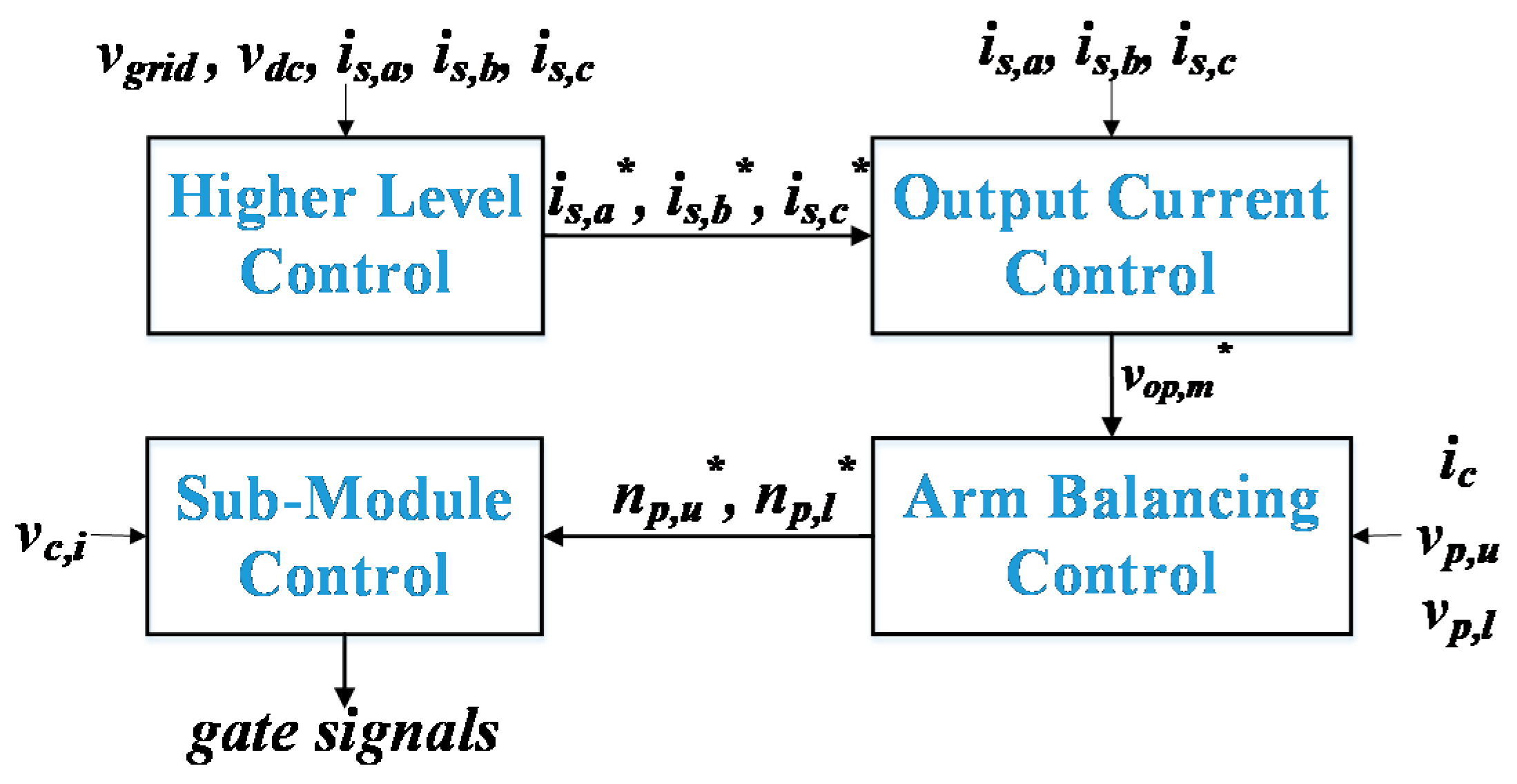
This paper is divided as follows: Firstly, the MMC topology along with its control hierarchy is presented in
Section 2, with particular emphasis on the capacitor voltage balance control. In
Section 3, the proposed mapping strategy is described.
Section 4 aims to show the simulation results in both normal and faulty conditions. HIL results are achieved by using a Xilinx System-on-Chip (SoC) Zynq-7000 in
Section 5. The real execution time for the bubble sorting algorithm, the max/min approach and the proposed strategy is also shown. Finally, the conclusions are drawn.
3. Description of the Proposed Capacitor Voltage Mapping Strategy
As highlighted before, in order to achieve a balance between the capacitor voltages, a ranking is firstly needed. In this section the CVMS is deeply discussed. In comparison with [
9] the choice of the voltage range is discussed, and the optimal values are found. Moreover, some improvements and a complexity evaluation are carried out.
3.1. Functional Principle
Normally the sorting methods, already proposed in literature, work with these fundamental steps:
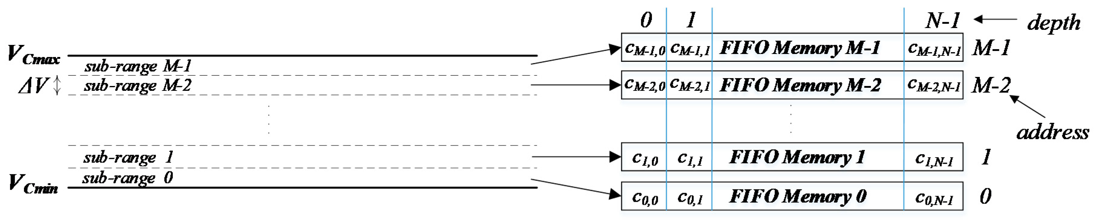
On the contrary, the proposed CVMS acts between the first and the second step. The idea is to directly store the SM positions in the right order, avoiding further manipulations. The strategy consists in dividing the capacitor voltage operating range in different sub-ranges, and assigning each sub-range to a memory location.
Then, only the SM positions (named here Pi) are stored in the memory according to their corresponding sub-ranges. In this way a quasi-sorted list is achieved right after reading the analogue-to-digital conversion of the capacitor voltage.
In normal operation, the SM capacitor voltages are between a minimum and maximum value,
and
, respectively. These two values can be evaluated when the MMC design is performed. The operation range of the capacitor voltage is divided into M sub-ranges with amplitudes equal to:
Each sub-range is mapped in a specific FIFO memory array as shown in
Figure 4. Therefore, all the SMs with the capacitor voltage that falls in the sub-range 0 are mapped in the FIFO memory at address 0; all the SMs with the capacitor voltage in the sub-range 1 in the address 1; and so on. Then, the number of sub-ranges can be seen as an address ADDR of the FIFO memories.
Firstly, a position number
Pi is assigned for each SM based on its physical placement in the arm. Then, it is stored along with the SM status (inserted or bypassed) in the cell
cADDRi,k, according to the address
ADDRi, and the status of the FIFO memory
k, that takes into account how many positions are already stored in the FIFO memory
i. The number of sub-ranges
M defines how many FIFO memories are required. Their depth has been chosen equal to the number of SMs
N in order to allow for storing all the positions in one FIFO memory when the capacitor voltages are close to each other. However, this FIFO depth can be optimized as described in [
9]. The bit-length of each memory cell has to be larger or equal to the size of the SM position
Pi plus the status bit.
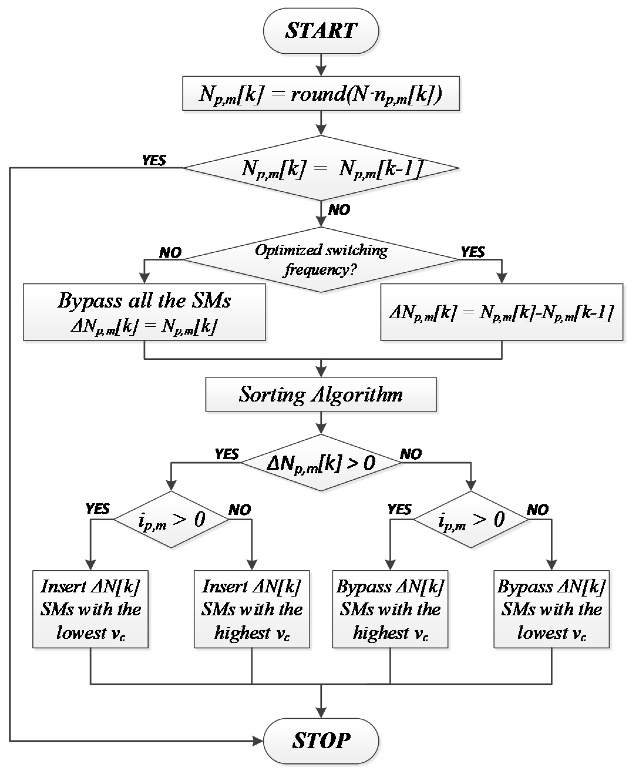
The SMs are normally inserted or bypassed accordingly to the NLC, i.e., when the insertion indices np,u and np,l, given in Equation (1) change. However, in order to avoid exceeding the capacitor voltage band during faults, some precautions should be considered. In addition to the normal insertion or bypass of the SMs according to the NLC, a swap is performed if an SM capacitor voltage reaches the last or the first voltage sub-range. The swap involves bypassing the SM that has reached the first or the last memory location, and inserting another SM accordingly to the mapping strategy.
3.1.1. Address Evaluation
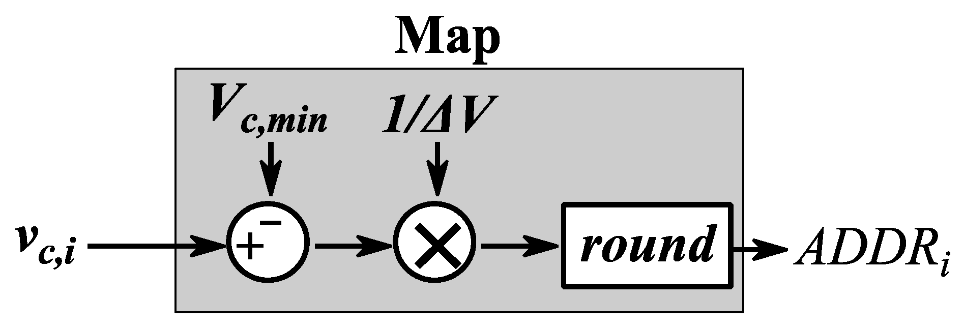
In this paragraph the way to perform an efficient mapping of the SMs into the memory is presented. The memory address
ADDRi is obtained by scaling the capacitor voltage
. The minimum capacitor voltage
(which is an MMC design criteria) is subtracted from the measured voltage
. The result is firstly divided by the amplitude of the sub-ranges Δ
V and then rounded in order to obtain an address, as shown in
Figure 5.
Pi is then stored in the memory according to the evaluated address.
3.1.2. Reading Operation
The SMs to be inserted or bypassed are obtained by reading the FIFO memories from the top (bottom) if the SMs with the highest (lowest) capacitor voltages are needed, according to the flowchart in
Figure 3. When a FIFO memory is empty, the memory located at the next address must be read.
3.1.3. Vcmin and Vcmax Evaluation
Vcmin and
Vcmax can be chosen, either equal to the maximum voltage of the capacitors, or by evaluating the maximum capacitor voltage ripple. In the first case, the proper behavior is ensured for each condition; however, by considering the same amplitude of the sub-ranges, a higher amount of memory is required. On the other hand, the second case can reduce the hardware resources, but a more detailed study should be accomplished. Moreover, once having evaluated the maximum ripple, a safety tolerance must be added to ensure good behavior during fault conditions. From [
24], the energy in the upper and lower arm can be evaluated:
where
WΣ and
WΔ are the per-phase energy and the imbalance energy, respectively. They are equal to:
with:
Being the pole-to-pole dc bus, the fundamental angular frequency, the phase angle, and the peak value of the fundamental output voltage and current, respectively.
Then, by replacing Equations (3) to (8) into
and
presented in Equations (11) and (12), the sum of the capacitor voltages for the upper arm and for the lower arm can be determined:
Finally, the capacitor voltage ripple can be expressed as:
Based on the evaluated ripple, the Vmax and Vmin can be chosen. In the following, a safety tolerance of 20% is also considered. It is worth noting that Vmax and Vmin are pre-evaluated and considered constant in this paper.
3.1.4. Accuracy and Complexity Evaluation
The achieved capacitor voltage balancing depends on the amplitude of the sub-ranges Δ
V. It is then also correlated to the available memory. As already said, from the CVB point of view, the small deviations among the capacitor voltages are not of interest. It is rather crucial not to exceed the safety limit of the capacitor voltage. This concept is already adopted in literature in order to optimize the switching frequency in the NLC [
8]. It allows to the capacitor voltages to freely vary inside a given band, performing extra switching only when the band is going to be exceeded. Therefore, a proper compromise can be guaranteed between the right CVB behavior and the memory usage. An M comprising between 8 and 64 can achieve this objective.
Concerning the complexity, the bubble sorting algorithm has the highest complexity equal to
O(
N2), where
O defines an upper bound of the running time of the algorithm. On the other hand, the max/min approach has a complexity equal to
O(N). Regarding the CVMS, it is equal to
O(N) only when
M ≪
N. Indeed, if
M is comparable with
N, the time for reading the memory becomes comparable with the time for writing in the memory. This is due to the fact that it is easier to find empty FIFO memories, and it requires more often an update of the address. These results are summarized in
Table 1.
4. Simulation Results
In this section the proposed CVMS is validated, and its advantages are highlighted compared to the popular bubble sorting algorithm and the fast max/min technique. In order to demonstrate the benefits of the proposed method, the MMC has been simulated in both normal and faulty conditions. The simulations have been performed in a PLECS
® power electronic simulation environment. The MMC and grid parameters are given in
Table 2 and
Table 3, respectively.
All the three methods: Bubble sorting, max/min and the proposed sorting approach, have been implemented in PLECS
®. Concerning the max/min approach, the one proposed in [
13] has been implemented in this paper. Its tolerance band has been set to 2 kV. Concerning the proposed mapping strategy, the adopted parameters are summarized in
Table 4. At the beginning the system is in the steady state condition.
The phase-to-ground fault is simulated at 0.7 s and removed at 0.8 s. When a fault occurs, the control requires to suddenly insert or bypass more SMs in the next sampling period. In this case, an algorithm that provides a fully sorted list (such as BSA) can enhance the dynamic performance of the converter. Indeed, it can allow the insertion (or the bypass) of the required SMs in only one sampling period. On the contrary, a max/min approach can insert only 1 SM, and then a number of sampling periods equal to the required SMs have to be intervened before the required control action is achieved. It might be executed in a repetitive manner during the same sampling period, but in this way the BSA is resulted.
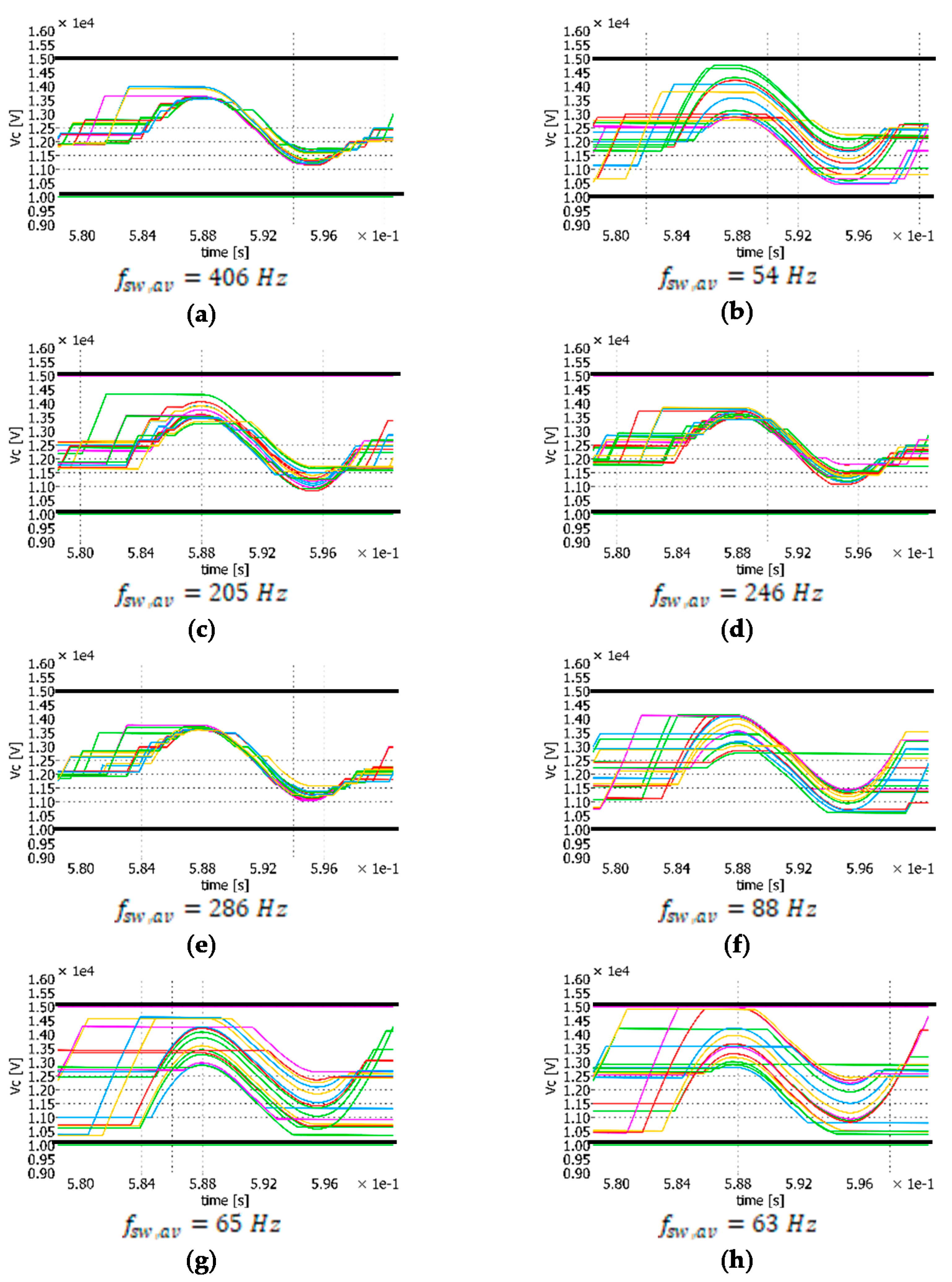
4.1. Impact on Voltage Balance and Switching Frequency
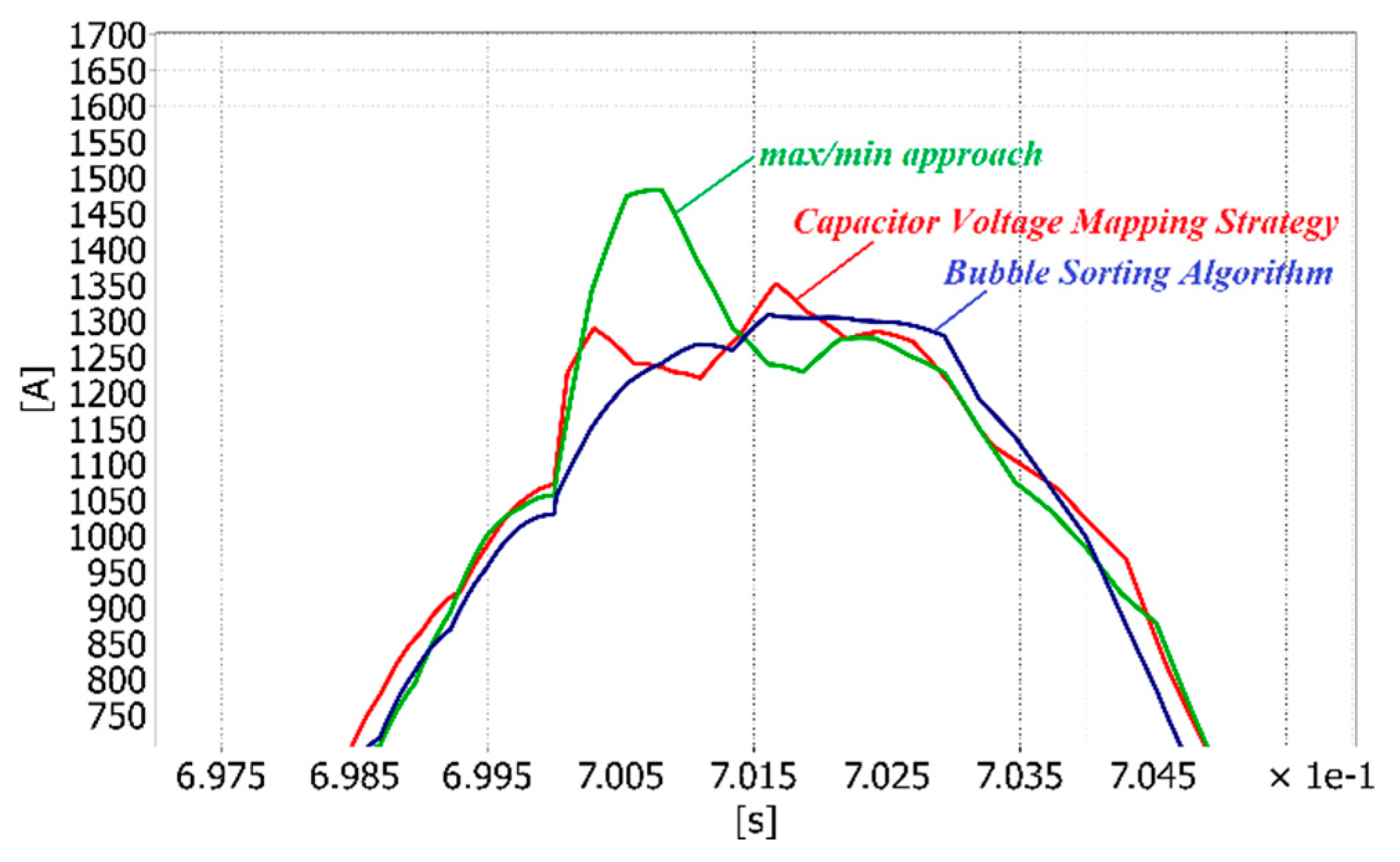
Firstly, a comparison in terms of capacitor voltage balance and achieved switching frequency is made among the implemented methods before the fault occurs.
Figure 6 shows the capacitor voltages obtained with: Bubble sorting algorithm, max/min approach, and capacitor voltage mapping strategy in the case of
, with and without the optimization of the switching frequency. The bubble sorting algorithm is executed each time there is a change in the insertion index
, and the selection technique always selects the best suitable SM which leads to the best voltage balancing at the cost of a high switching frequency.
On the other hand, the max/min approach intrinsically optimizes the switching frequency; indeed, it just selects 1 SM to be inserted (or bypassed) each time there is a change in
. The proposed technique is executed with and without the switching frequency optimization (refers to
Figure 3). From
Figure 6c to
Figure 6e the switching frequency optimization is off, and then the best SMs are inserted every time.
On the contrary, the last three plots of
Figure 6 consider an optimized selection method that insert or bypass only the required SMs at the same time. The proposed strategy without the optimized selection technique tends to the balancing achieved with the BSA when the number of sub-ranges M increases. However, in this last case, the resulted average switching frequency (
) is unacceptably high. Then, the switching frequency optimization can be taken into consideration. In this case, the achieved voltage balancing is degraded, but the capacitor voltages are kept between the acceptable boundaries (straight black lines in
Figure 6). Moreover, by increasing M it is possible to improve the switching frequency at the cost of a small increase in the required memory of the controller.
Finally, it can be concluded that the proposed strategy well balances the capacitor voltages in normal conditions like the other two methods. Moreover, the achieved switching frequency is close to the one obtained with the max/min approach, but a complete sorted list is performed. The number of sub-ranges M can be chosen according to the application under study. In the following, the optimized switching frequency method and M = 8 are considered.
4.2. Performance during Phase-to-Ground Fault
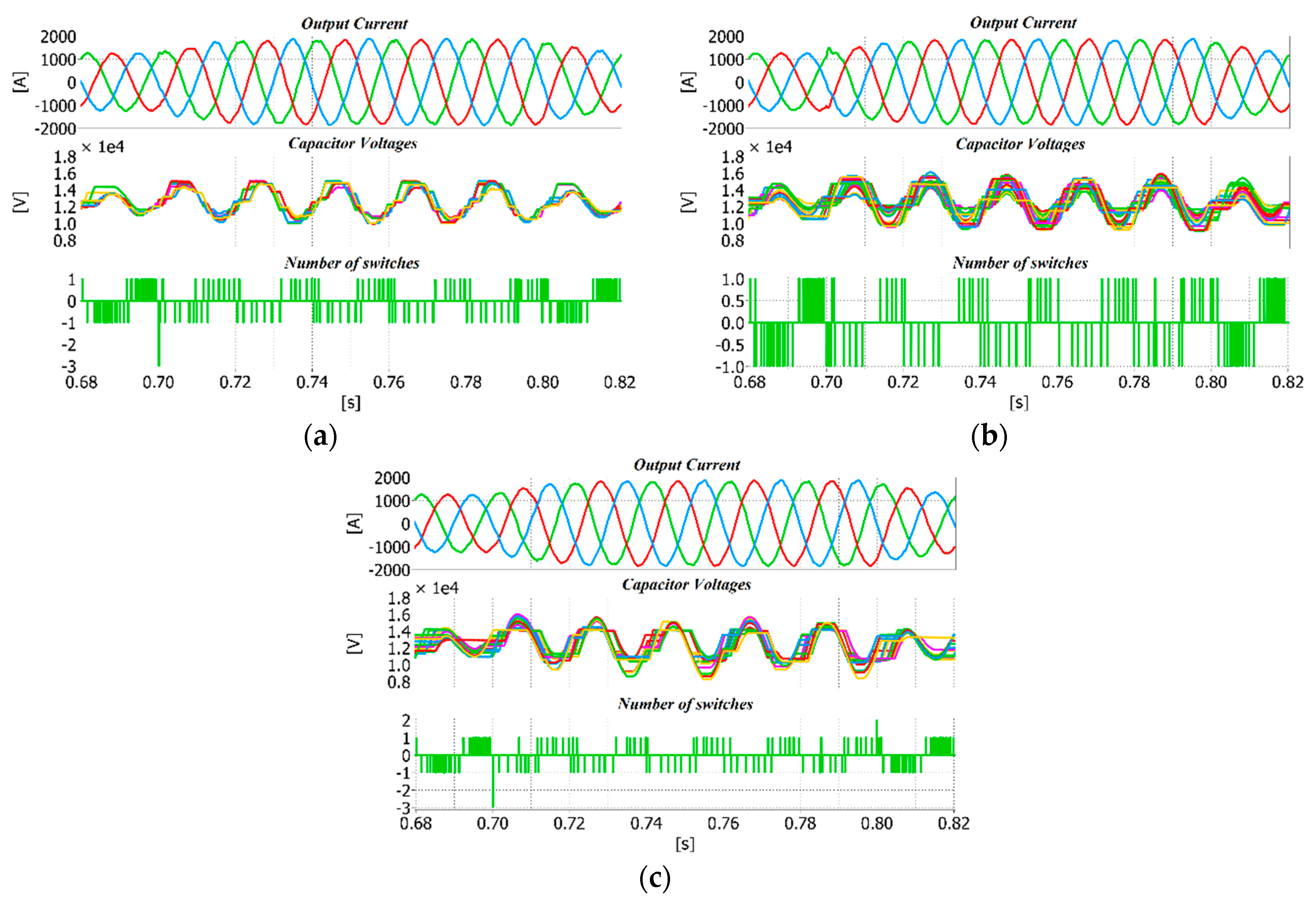
Figure 7 shows the output currents, the capacitor voltages and the required number of switches for the upper arm of phase
a in the case of the bubble sorting algorithm, the max/min approach and the proposed mapping strategy before, during and after the phase-to-ground fault. The fault occurs at 0.7 s, and it is removed at 0.8 s. At the moment of the fault, 3 SMs have to be bypassed for this example.
Figure 8 shows a zoom of the output current at the time of the fault. It is worth noting that the output current achieved with the max/min approach has an overshoot caused by the slower dynamic response of the controller.
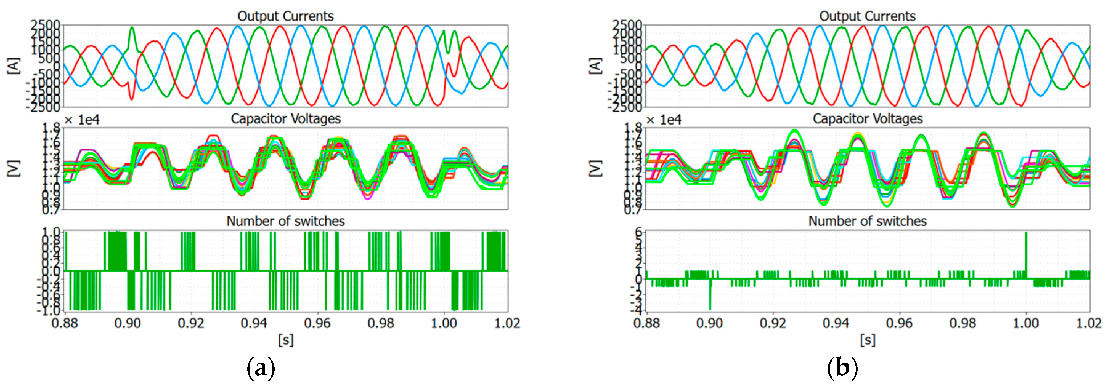
4.3. Performance during Line-to-Line Fault
A line-to-line fault between phase a and phase b has been also simulated in a PLECS
® environment. The fault occurs at 0.9 s and is removed at 1.0 s. The output currents, capacitor voltages and the number of required switches are shown in
Figure 9 for both max/min approach,
Figure 9a, and the proposed capacitor voltage mapping strategy,
Figure 9b.
Like in the case of phase to ground fault, the max/min approach slows down the dynamic response of the controller by causing an overshoot of the output current, as it can be seen in
Figure 9a. On the other hand, the proposed technique is able to bypass 4 SMs at the same time when the fault occurs by then providing a faster dynamic response and avoiding overshoots on the output currents.
The good behavior of the proposed mapping strategy has been demonstrated with a different number of sub-ranges M. Moreover, the phase-to-ground fault and the phase-to-phase fault have been considered in order to show the limits of the max/min approach. The latter allows a very low execution time, and an easy implementation at the expense of a slower response of the controller during fault conditions. The proposed technique, instead, does not affect the control dynamic, still keeping the execution time low, as shown in the next section.
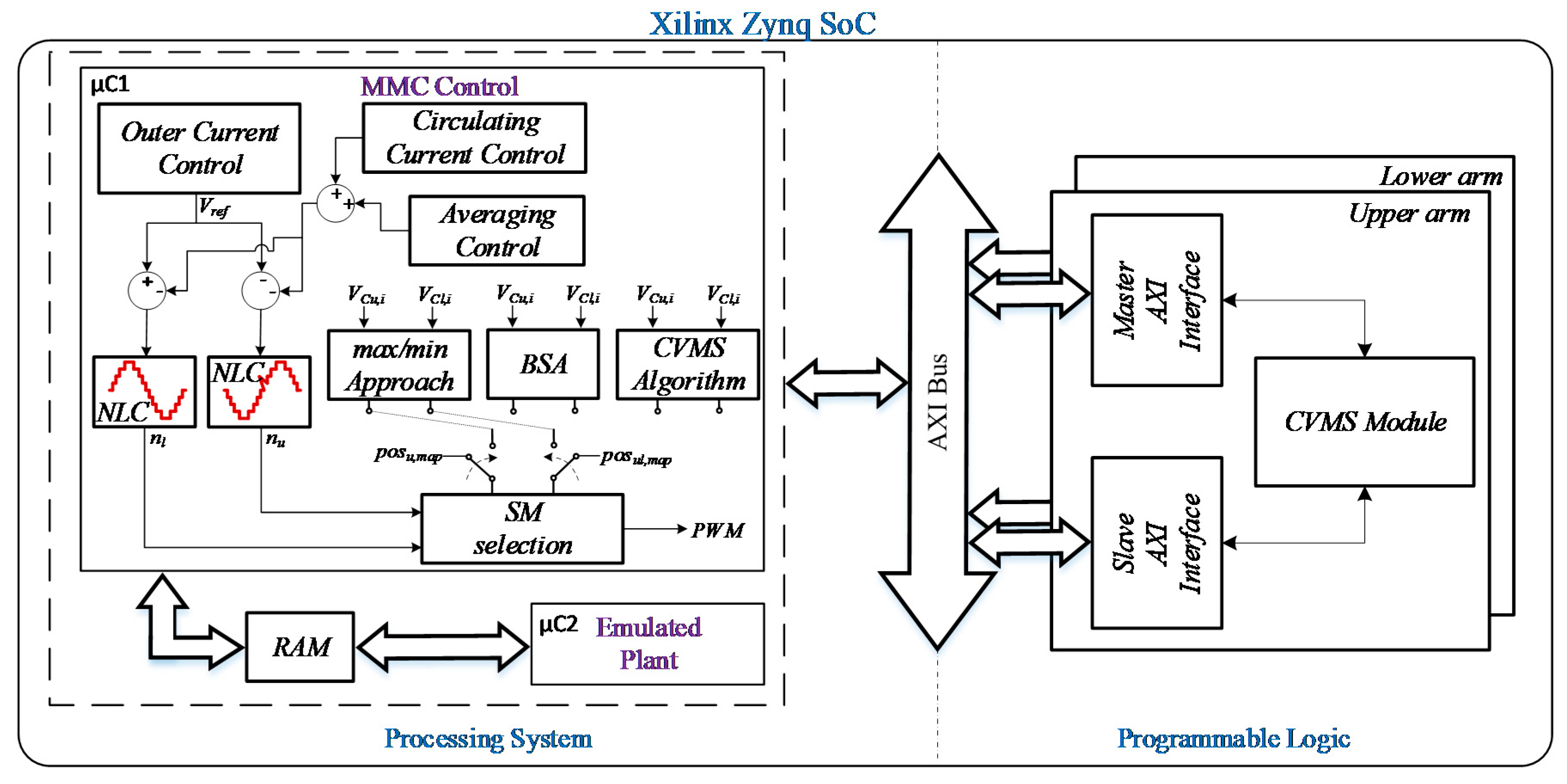
5. HIL Results
Due to the fact that the realization of large MMC (consisting of hundreds of modules) systems are very expensive, a common approach to test the behavior of the control system is the use of the HIL approach. In this section HIL results have been provided in order to evaluate the implementation requirements, show the proper behavior of the proposed strategy. and compare it with the bubble sorting algorithm and the max/min approach in terms of the achieved execution time. For the HIL system the Digilent Zedboard mounting a Xilinx SoC Zynq-7000 device (named in the following simply Zynq) has been adopted. The adopted Zynq consists of two embedded ARM Cortex processors, 85,000 logic cells, 4.9 Mb block RAM and 220 DSP slices. It is as shown in
Figure 10. The MMC control is implemented in the first processor, along with the three sorting methods. The emulated plant is instantiated in the second processor. The proposed CVMS technique is also implemented in the programmable logic in order to enhance its inherent parallelism, and then reduce the execution time. The processor system and the programmable logic communicate through the AXI bus. A single-phase MMC model, with
N = 64 and based on [
26], is implemented in the second processor.
The case of
N = 64 is realistic in view of an industrial application. The SM capacitors are equal to 2.4 mF and the output energy of 500 kW is dissipated on a resistive load. The remaining MMC parameters are equal to the ones presented in
Table 2.
It is worth it to note here that the implementation of a three-phase system requires a huge amount of hardware resources for the real-time emulation of the plant, without adding anything to the performance analysis intended into this paper. Indeed, the considered single-phase controller can be seen as the phase controller of a three-phase system. In order to enhance the timing performance of the proposed CVMS, it has been also implemented in the Programmable Logic (PL) part of the SoC. The hardware architecture is depicted in
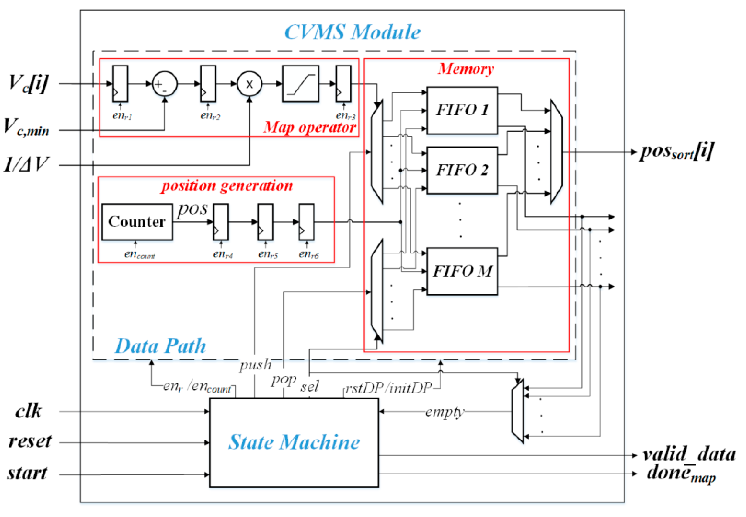
Figure 11.
It consists of a data path for treating the data, and a state machine for the synchronization. In the data path, the map operator, the position generator and the allocated memory, can be easily noted. The quasi-sorted list is sent to the controller through the AXI bus. The chosen AXI mode is the burst configuration, in order to decrease the latency due to the communication.
It is worth noting that the main controller can start its action as soon as it receives the first data, because the sent list is already sorted. Considering the BSA and the max/min approach, the controller should wait all the voltages in order to start the algorithms in the PS.
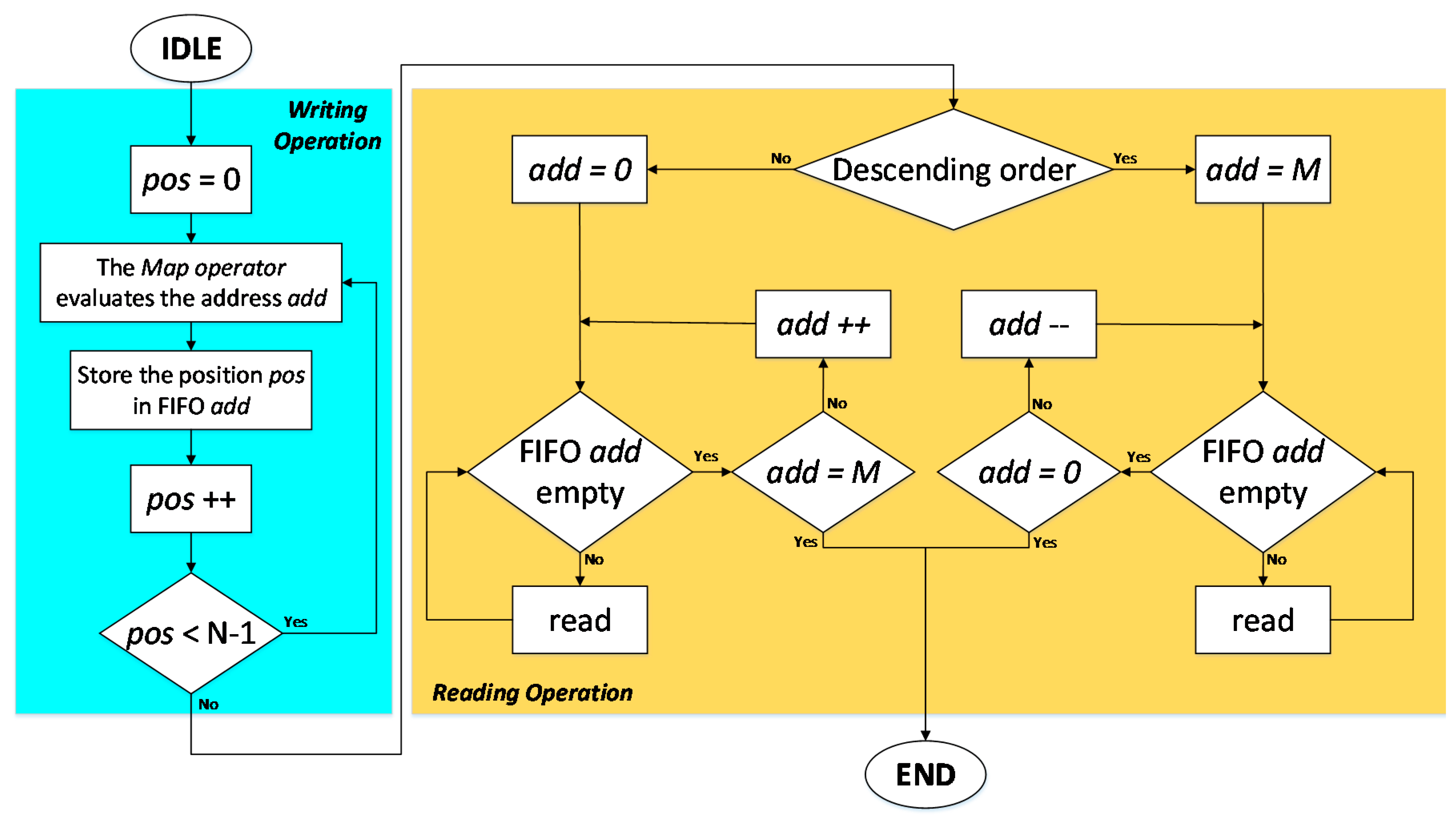
Figure 12 shows the flow chart of the state machine that controls the data path in
Figure 11. When the capacitor voltages are measured, the operation for writing the SM positions in the memory firstly starts. Then, the position pos is set to 0, and the map operator evaluates the address add corresponding to the first capacitor voltage. The position pos is stored in the FIFO memory add, and the value of pos is then increased. If it is still less than the number of SMs, the map operator is executed again. If pos is equal to N it means that all the capacitor voltages have been measured, and the SM positions have all been stored in the memory, and the writing operation is ended. At this point the reading operation starts, and the order direction is firstly checked. If a descending list is needed, the address add is set to M, and the FIFO memory add is read until it is empty. When this happens, the value of add is decreased and then the next FIFO memory can be read. This operation lasts until the value of add is equal to 0. On the other hand, if an ascending list is required, add is set to 0, and each time the FIFO memory add is empty, its value is increased. In this case the operation ends when add is equal to
M.
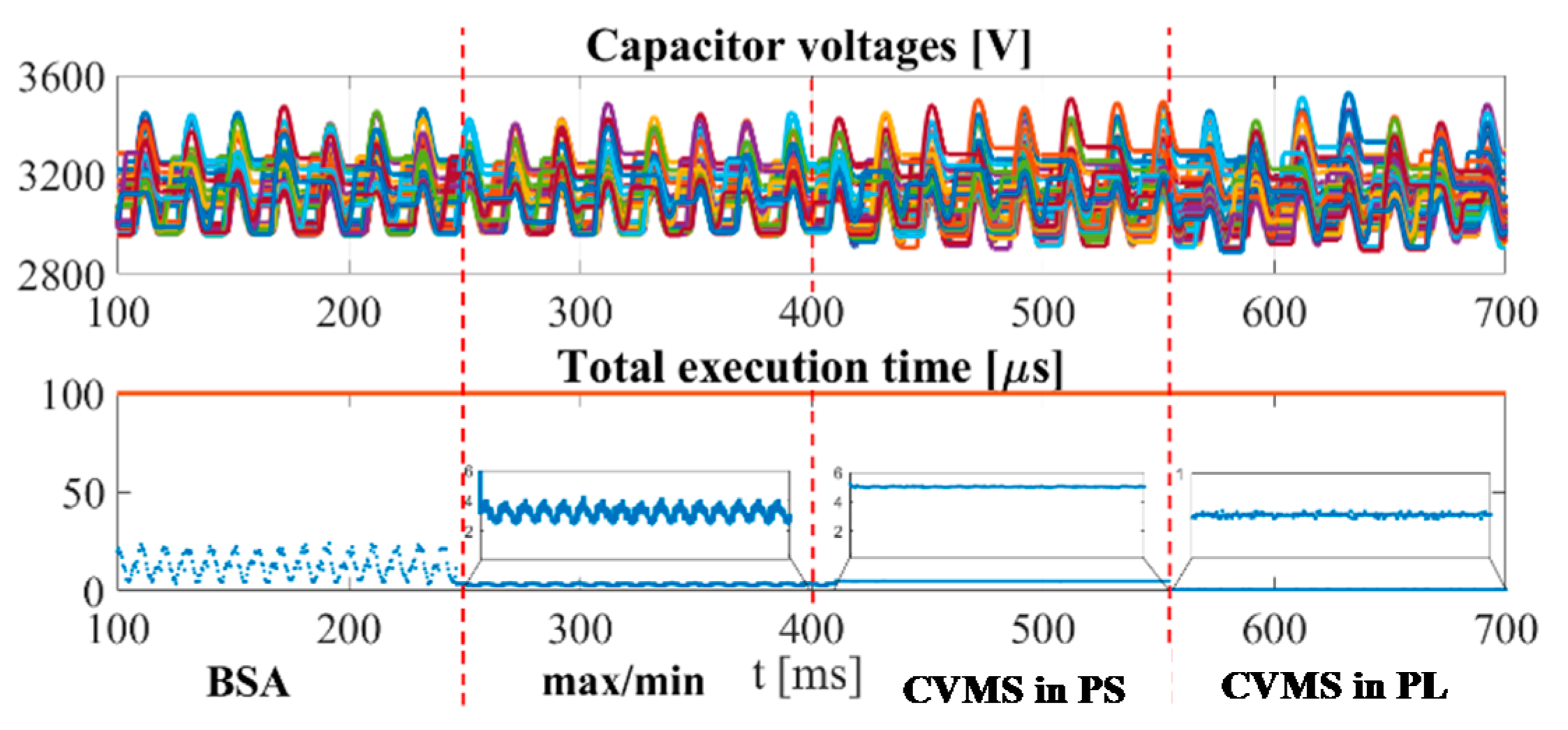
Figure 13 shows the capacitor voltages and the execution time for the bubble sorting algorithm, the max/min approach, the CVMS implemented in the processor system and in the programmable logic. These results have been achieved by changing in real-time the sorting technique by using the push buttons provided on the Zynq development board.
A serial communication protocol has been employed to read the internal signals and display them on the PC. The achieved execution times are summarized in
Table 5. It is noteworthy that the execution time of the CVMS in PS is comparable with the one obtained with the max/min approach, but it provides a quasi-sorted list useful for enhancing the controller performance, as shown in the previous section. Besides, if the PL solution is adopted, thanks to the exploitation of the inherent algorithm parallelism, its execution time can be reduced, further achieving the best timing performance, and still keeping the controller dynamic. The required resources for the proposed mapping strategy implemented in the PL part are summarized in
Table 6. It is worth it to note that the required memory is less than the 3% of the available memory on the Zynq platform. Then, it is possible to conclude that a faster capacitor voltage balancing algorithm is achieved by preserving the controller dynamic during fault, and that without significantly increasing the required resources.

 ,
, 


