Transversely Compact Single-Ended and Balanced Bandpass Filters with Source–Load-Coupled Spurlines


Abstract
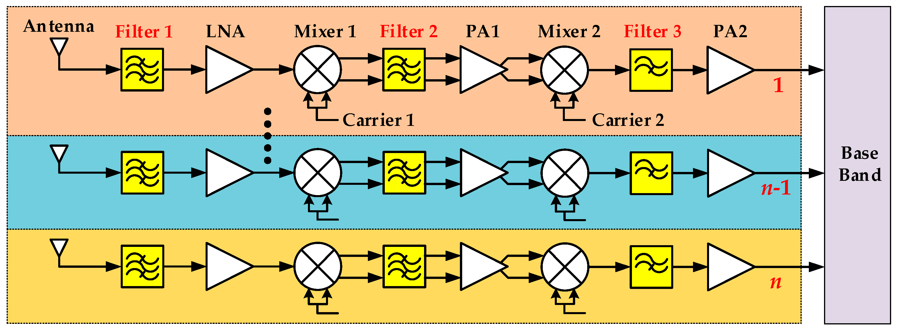
:1. Introduction
2. Basic Elements of the Proposed Filters
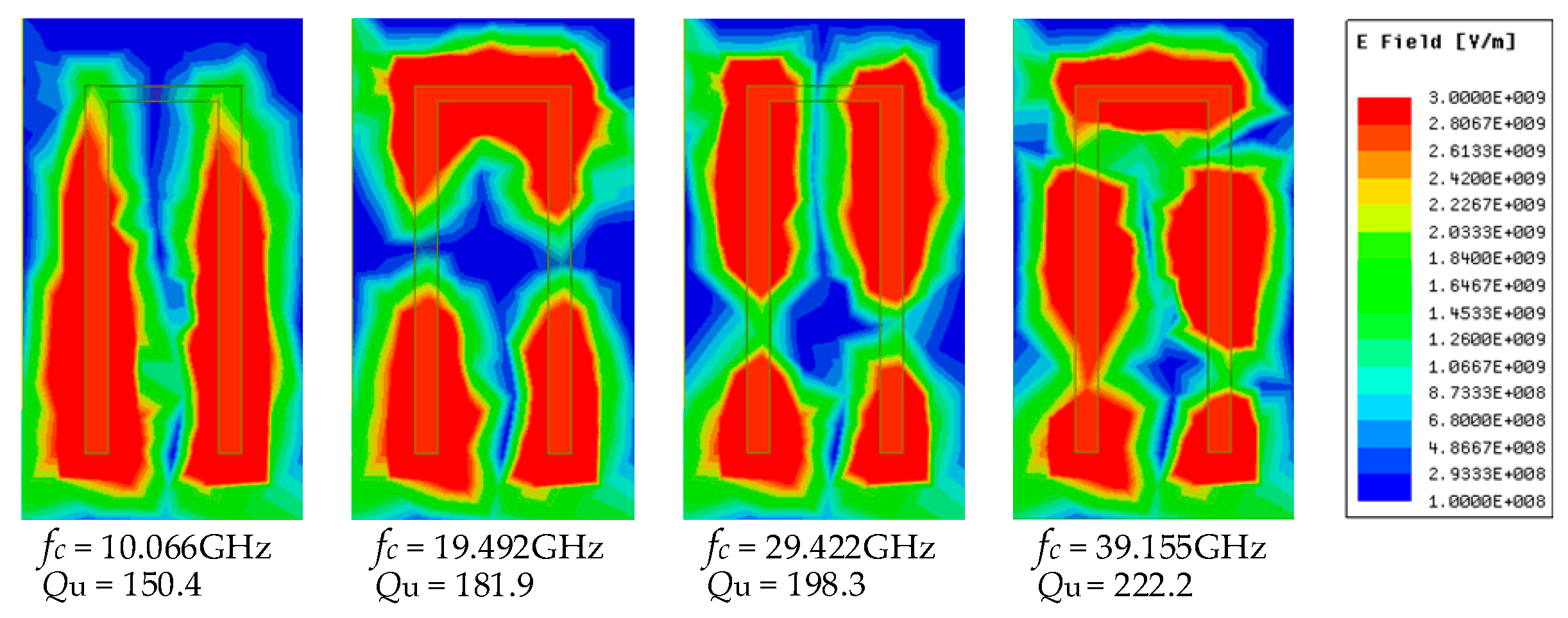
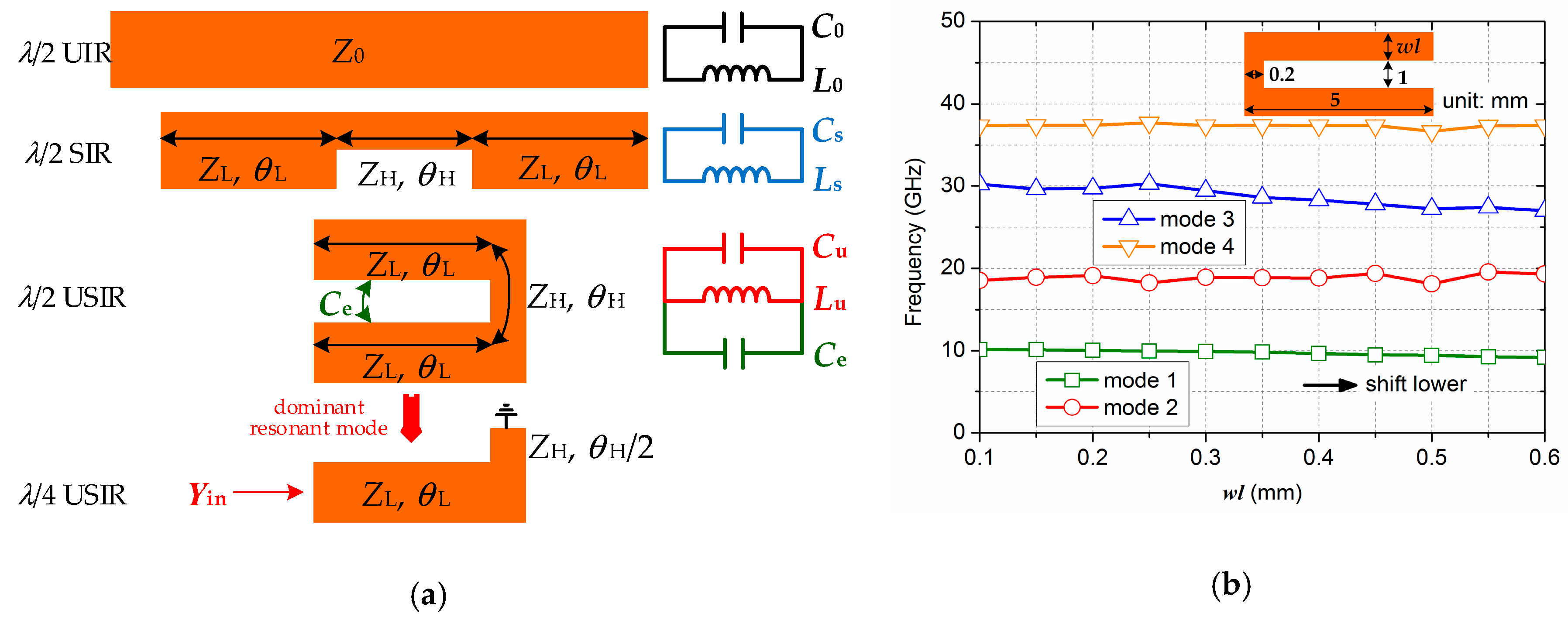
2.1. Half-Wavelength U-Shaped Stepped Impedance Resonator
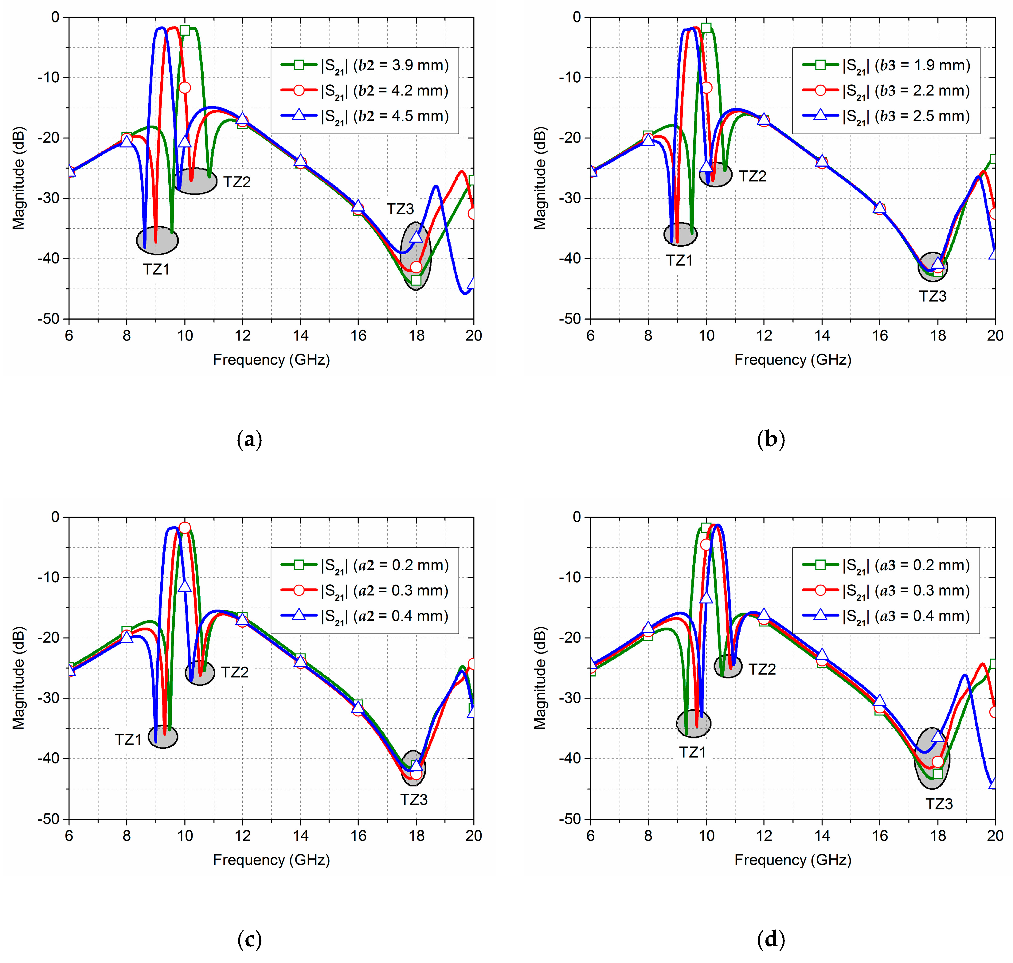
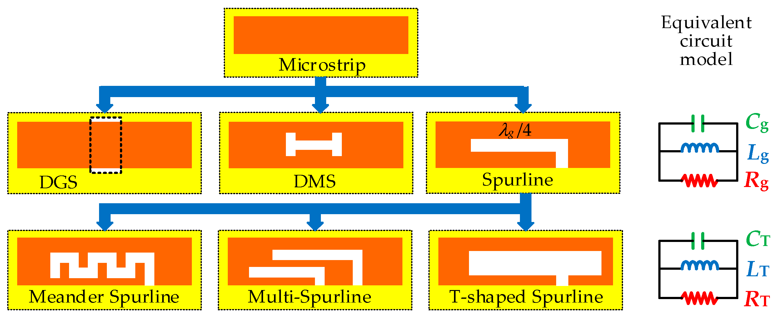
2.2. T-Shaped Spurline
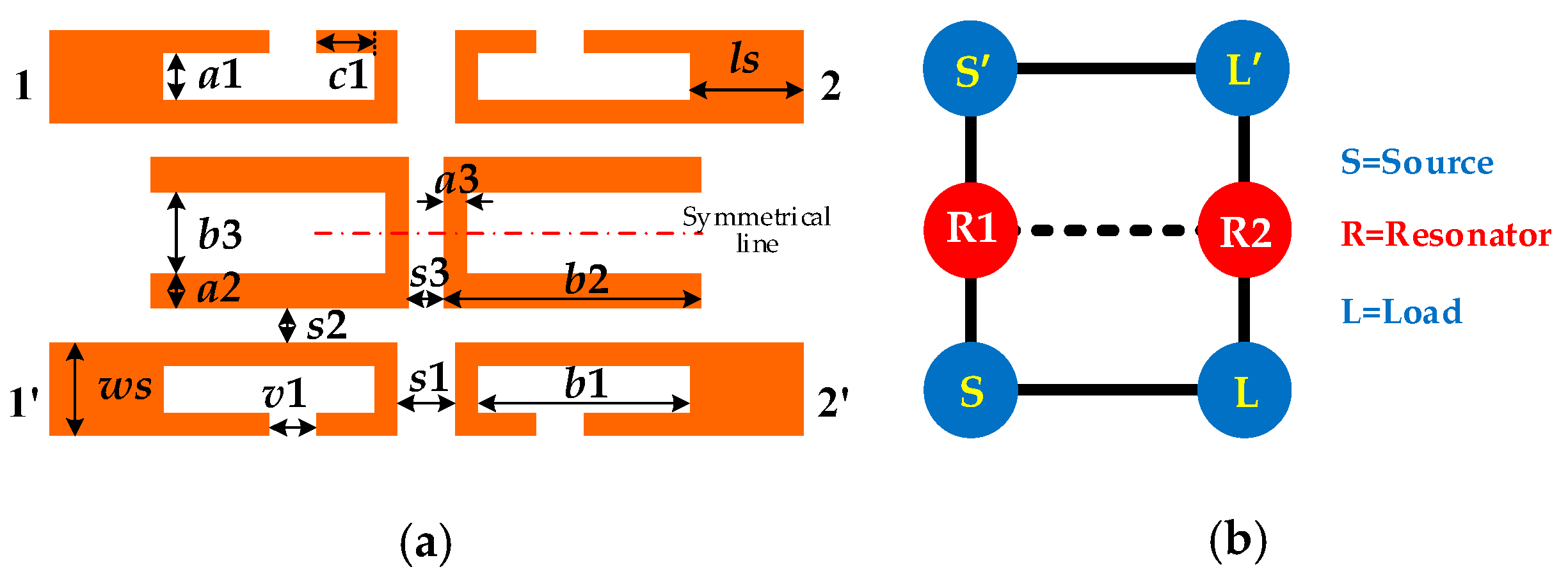
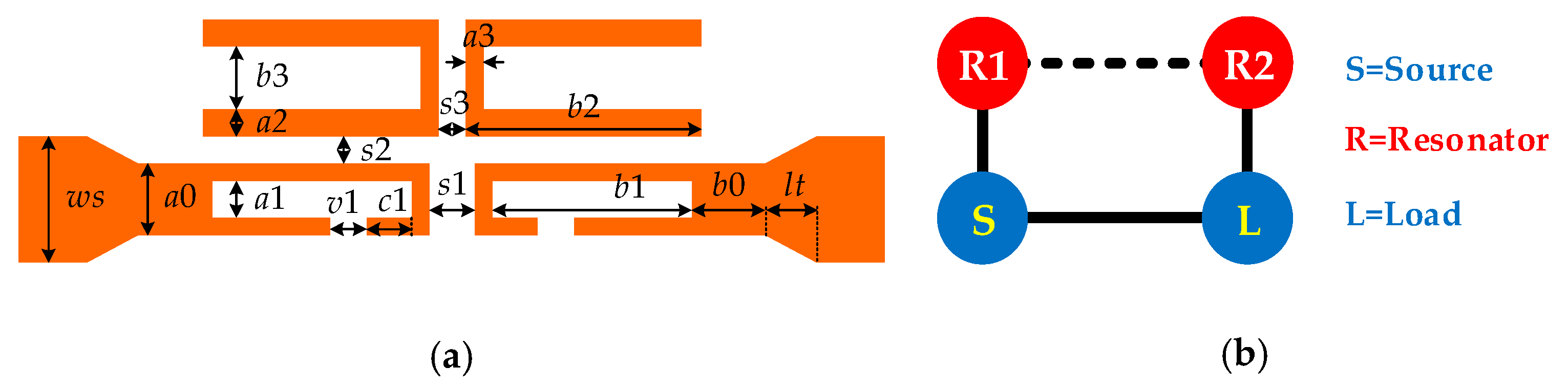
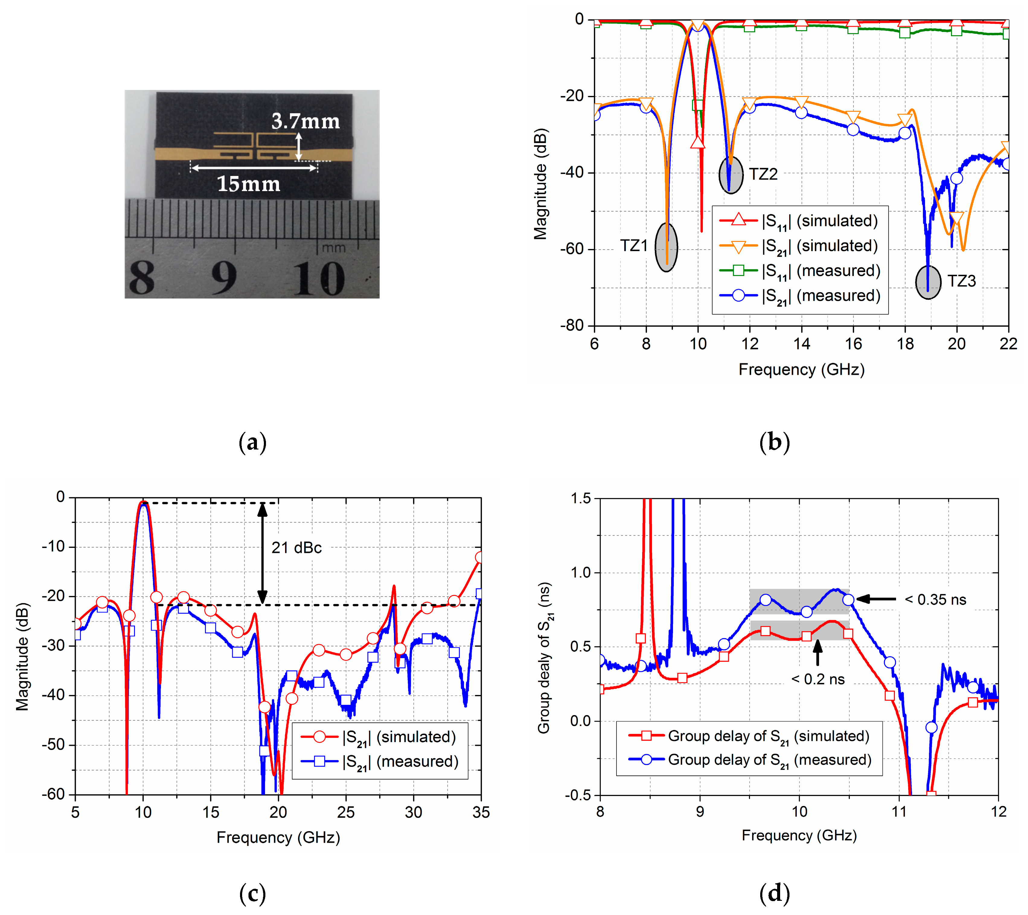
3. Single-Ended Bandpass Filter with Source–Load-Coupled Spurlines
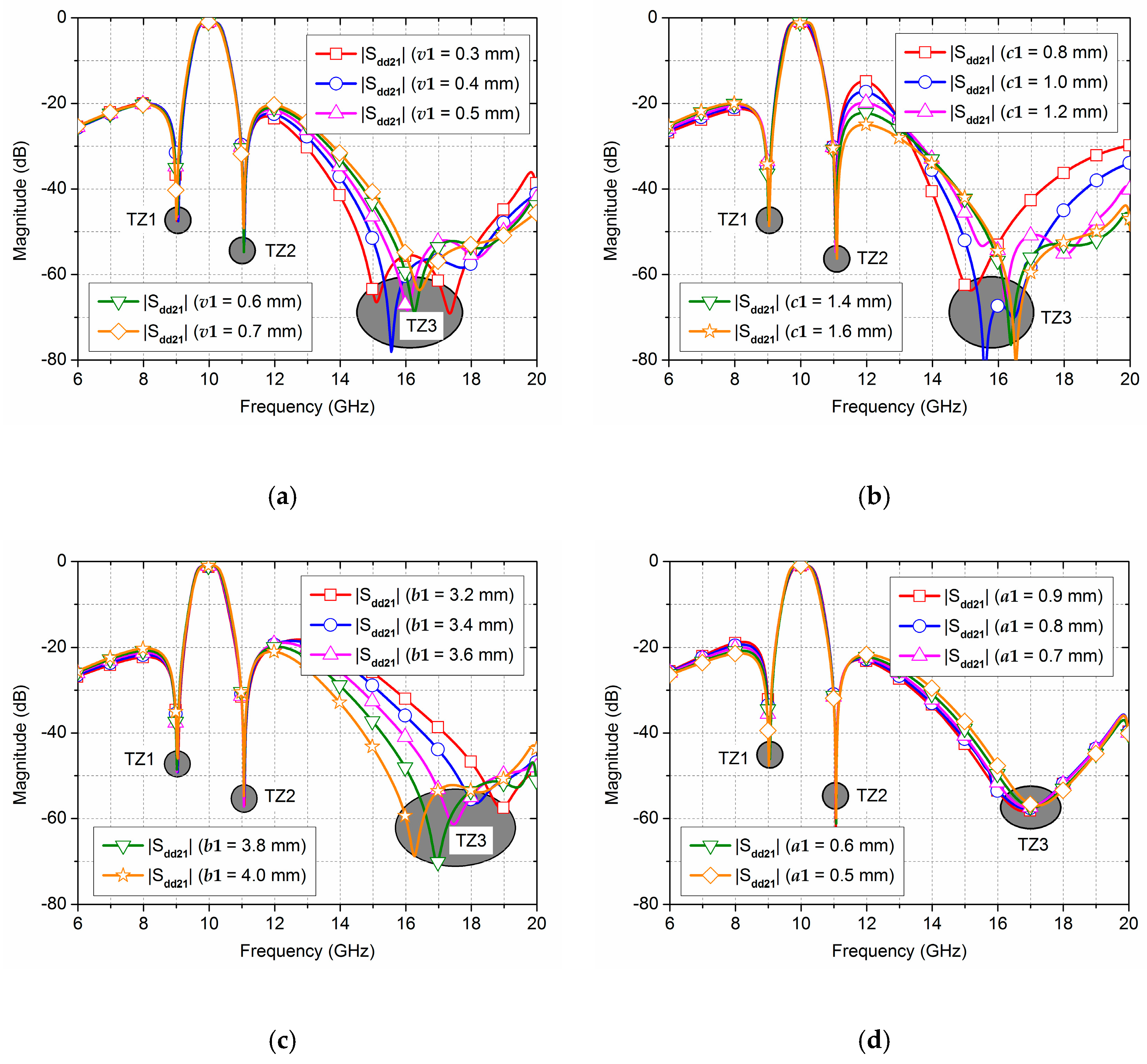
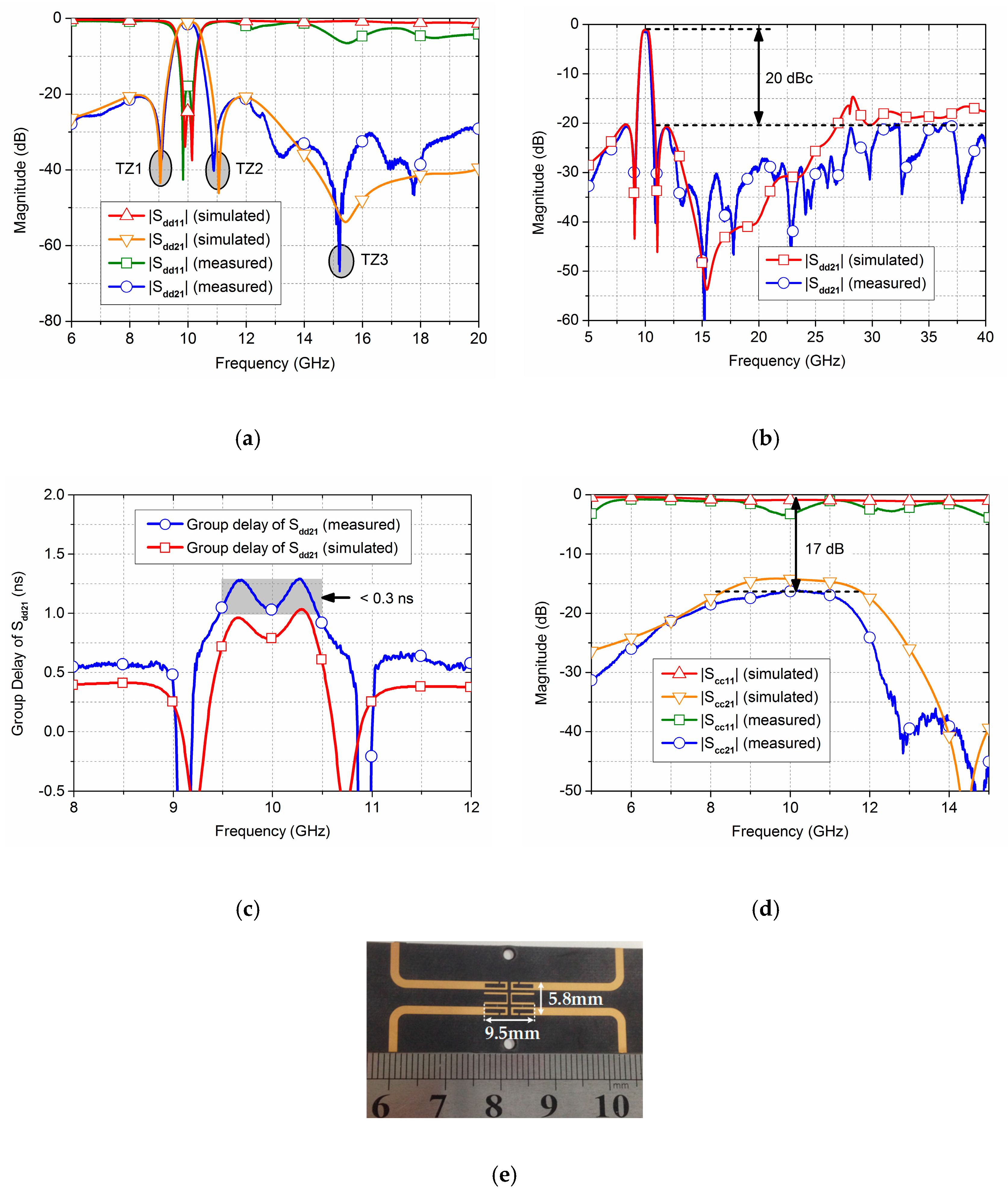
4. Balanced Bandpass Filters with Source–Load-Coupled Spurlines
5. Discussion
6. Conclusions
Author Contributions
Funding
Conflicts of Interest
References
- Rebeiz, G.M.; Entesari, K.; Reines, I.C.; Park, S.J.; Eltanani, M.A.; Grichener, A.; Brown, A.P. Tuning in to RF MEMS. IEEE Microw. Mag. 2009, 10, 55–72. [Google Scholar] [CrossRef]
- Pozar, D.M. Microwave Engineering, 4th ed.; Wiley: New York, NY, USA, 2012; pp. 48–89. ISBN 978-0-470-63155-3. [Google Scholar]
- Makimoto, M.; Yamashita, S. Bandpass filter using parallel coupled stripline stepped impedance resonators. IEEE Trans. Microw. Theory Tech. 1980, 28, 1413–1417. [Google Scholar] [CrossRef]
- Pinel, S.; Bairavasubramanian, R.; Laskar, J.; Papapolymerou, J. Compact planar and vialess composite low-pass filters using folded stepped-impedance resonator on liquid-crystal-polymer substrate. IEEE Trans. Microw. Theory Tech. 2005, 53, 1707–1712. [Google Scholar] [CrossRef]
- Roychoudhury, S.; Parui, S.K.; Das, S. Improvement of stopband using a spiral defected microstrip and defected ground structures. In Proceedings of the IEEE Applied Electromagnetics Conference, Kolkata, India, 18–22 December 2011. [Google Scholar]
- Liu, H.; Knoechel, R.H.; Schuenemann, K.F. Miniaturized bandstop filter using meander spurline and capacitively loaded stubds. ETRI J. 2007, 29, 614–618. [Google Scholar] [CrossRef]
- Liao, C.K.; Chang, C.Y. Design of microstrip quadruplet filters with source-load coupling. IEEE Trans. Microw. Theory Tech. 2005, 53, 2302–2308. [Google Scholar] [CrossRef]
- Liu, H.; Liu, F.; Guan, X.; Ren, B.; Liu, T.; Wang, Y.; Xu, H. Wide-stopband superconducting bandpass filter using slitted stepped-impedance resonator and composite spurline structure. IEEE Trans. Appl. Supercond. 2018, 28, 1501508. [Google Scholar] [CrossRef]
- Ponchak, G.E. Coplanar stripline spurline stub resonators with even-mode suppression for bandpass and bandstop filters. IEEE Microw. Wirel. Compon. Lett. 2018, 28, 1098–1100. [Google Scholar] [CrossRef]
- Shi, J.; Xue, Q. Balanced bandpass filters using center-loaded half-wavelength resonator. IEEE Trans. Microw. Theory Tech. 2010, 58, 970–977. [Google Scholar]
- Fernandez-Prieto, A.; Qian, S.L.; Hong, J.; Martel, J.F.; Medina, F.; Mesa, F.; Naqui, J.; Martin, F. Common-mode suppression for balanced bandpass filters in multilayer liquid crystal polymer technology. IET Microw. Antennas Propag. 2015, 9, 1249–1253. [Google Scholar] [CrossRef]
- Sans, M.; Selga, J.; Velez, P.; Rodriguez, A.; Bonanche, J.; Borria, V.E.; Martin, F. Automated design of common-mode suppressed balanced wideband bandpass filters by means of aggressive space mapping. IEEE Trans. Microw. Theory Tech. 2015, 63, 3896–3908. [Google Scholar] [CrossRef]
- Zhang, W.; Wu, Y.; Liu, Y.; Yu, C.; Hasan, A.; Ghannouchi, F.M. Planar wideband differential-mode bandpass filter with common-mode noise absorption. IEEE Microw. Wirel. Compon. Lett. 2017, 27, 458–460. [Google Scholar] [CrossRef]
- Ebrahimi, A.; Baum, T.; Ghorbani, K. Differential bandpass filters based on dumbbell-shaped defected ground resonators. IEEE Microw. Wirel. Compon. Lett. 2018, 28, 129–131. [Google Scholar] [CrossRef]
- Sans, M.; Selga, J.; Velez, P.; Bonanche, J.; Rodriguez, A.; Borria, V.E.; Martin, F. Compact wideband balanced bandpass filters with very broad common-mode and differential-mode stopbands. IEEE Trans. Microw. Theory Tech. 2018, 66, 737–750. [Google Scholar] [CrossRef]
- Fernandez-Prieto, A.; Lujiambio, A.; Martel, J.; Medina, F.; Mesa, F.; Boix, R.R. Balanced-to-balanced microstrip diplexer based on magnetically coupled resonators. IEEE Access 2018, 6, 18536–18547. [Google Scholar] [CrossRef]
- Gomez-Garcia, R.; Munoz-Ferreras, J.M.; Feng, W.; Psychogiou, D. Balanced symmetrical quasi-reflectionless single- and dual-band bandpass filters. IEEE Microw. Wirel. Compon. Lett. 2018, 28, 798–800. [Google Scholar] [CrossRef]
- Feng, W.; Zhao, Y.; Che, W.; Gomez-Garcia, R.; Xue, Q. Single-ended-to-balanced filtering power dividers with wideband common-mode suppression. IEEE Trans. Microw. Theory Tech. 2018, 66, 5531–5542. [Google Scholar] [CrossRef]
- Sagawa, M.; Makimoto, M.; Yamashita, S. Geometrical structure and fundamental characteristics of microwave stepped-impedance resonators. IEEE Trans. Microw. Theory Tech. 1997, 45, 1078–1085. [Google Scholar] [CrossRef]
- Ting, H.-L.; Hsu, S.-K.; Wu, T.-L. Broadband eight-port forward-wave directional couplers and four-way differential phase shifter. IEEE Trans. Microw. Theory Tech. 2018, 66, 2161–2169. [Google Scholar] [CrossRef]


| Ref. | f0, FBW 1 (GHz, %) | Insertion Loss (dB) | Number of TZ 2 | Stopband (dBc, n·f0) | CMRR 3 (dB) | Electrical Size (λ02/εr) |
|---|---|---|---|---|---|---|
| [11] | 4, 16 | 1.5 | 0 | 20, 2 | 30 | 0.510 |
| [13] | 2, 55.5 | 0.29 | 1 | N.A. | 25 | 0.329 |
| [15] | 1.9, 47.4 | 1.5 | 2 | 22, 3.4 | 28 | 0.251 |
| Ours | 10, 6.1 | 0.9 | 3 | 20, 4 | 16.1 | 0.128 |
© 2019 by the authors. Licensee MDPI, Basel, Switzerland. This article is an open access article distributed under the terms and conditions of the Creative Commons Attribution (CC BY) license (http://creativecommons.org/licenses/by/4.0/).
Share and Cite
Yan, F.; Huang, Y.M.; Huang, T.; Ding, S.; Wang, K.; Bozzi, M. Transversely Compact Single-Ended and Balanced Bandpass Filters with Source–Load-Coupled Spurlines. Electronics 2019, 8, 416. https://doi.org/10.3390/electronics8040416
Yan F, Huang YM, Huang T, Ding S, Wang K, Bozzi M. Transversely Compact Single-Ended and Balanced Bandpass Filters with Source–Load-Coupled Spurlines. Electronics. 2019; 8(4):416. https://doi.org/10.3390/electronics8040416
Chicago/Turabian StyleYan, Fang, Yong Mao Huang, Tao Huang, Shuai Ding, Kenian Wang, and Maurizio Bozzi. 2019. "Transversely Compact Single-Ended and Balanced Bandpass Filters with Source–Load-Coupled Spurlines" Electronics 8, no. 4: 416. https://doi.org/10.3390/electronics8040416
APA StyleYan, F., Huang, Y. M., Huang, T., Ding, S., Wang, K., & Bozzi, M. (2019). Transversely Compact Single-Ended and Balanced Bandpass Filters with Source–Load-Coupled Spurlines. Electronics, 8(4), 416. https://doi.org/10.3390/electronics8040416