Article

Electronic Circuit with Controllable Negative Differential Resistance and its Applications

1
Research and Development Department, Mathematical Modelling & Research Holding Limited, London W1W 7LT, UK
2
Department of Electronics, National Aviation University, 03058 Kyiv, Ukraine
3
Projects and Maintenance Section, The Private Department of the President of the United Arab Emirates, Abu Dhabi 000372, UAE
*
Author to whom correspondence should be addressed.
Electronics 2019, 8(4), 409; https://doi.org/10.3390/electronics8040409
Submission received: 5 March 2019 / Revised: 2 April 2019 / Accepted: 3 April 2019 / Published: 8 April 2019
(This article belongs to the Special Issue Intelligent Electronic Devices)

Abstract

:
Electronic devices and circuits with negative differential resistance (NDR) are widely used in oscillators, memory devices, frequency multipliers, mixers, etc. Such devices and circuits usually have an N-, S-, or Λ-type current-voltage characteristics. In the known NDR devices and circuits, it is practically impossible to increase the negative resistance without changing the type or the dimensions of transistors. Moreover, some of them have three terminals assuming two power supplies. In this paper, a new NDR circuit that comprises a combination of a field effect transistor (FET) and a simple bipolar junction transistor (BJT) current mirror (CM) with multiple outputs is proposed. A distinctive feature of the proposed circuit is the ability to change the magnitude of the NDR by increasing the number of outputs in the CM. Mathematical expressions are derived to calculate the threshold currents and voltages of the N-type current-voltage characteristics for various types of FET. The calculated current and voltage thresholds are compared with the simulation results. The possible applications of the proposed NDR circuit for designing single-frequency oscillators and voltage-controlled oscillators (VCO) are considered. The designed NDR VCO has a very low level of phase noise and has one of the best values of a standard figure of merit (FOM) among recently published VCOs. The effectiveness of the proposed oscillators is confirmed by the simulation results and the implemented prototype.

Graphical Abstract

1. Introduction

Nowadays, negative differential resistance devices and circuits are widely used in oscillators, memory, frequency dividers, and multiplier circuits [1,2,3,4,5]. The presence of negative resistance in an electrical circuit makes it possible not to dissipate electrical energy in the form of heat, but to generate electrical power, even if it has only two terminals and not three as in transistors. There are two types of negative resistance, namely, differential and static. Sometimes NDR is also called negative dynamic resistance. The NDR is the first derivative of the voltage relative to the current at the operating point. The current-voltage characteristics with NDR region can be created in two ways. The first way involves the use of special electronic devices, such as a Gunn diode, a tunnel diode, three-terminal graphene NDR devices [6], and others. In the second way, the current-voltage characteristics with NDR region are created artificially with the help of special electronic circuits. However, the known NDR electronic circuits have some disadvantages that limit their use. Let us consider the well-known electronic circuits with NDR. The studies [7,8] considered the NDR circuit based on complementary metal-oxide-semiconductor (CMOS) NDR inverters requiring two power supplies. Thus, to create the current-voltage characteristics with NDR region three terminals should be used. The study [9] considered an electronic oscillator based on a bipolar junction transistor (BJT)-metal-oxide-semiconductor field-effect transistor (MOSFET) structure with Λ-type current-voltage characteristics and two power supplies. The study [10] considered an NDR circuit composing three resistors and two BJT. The N-type current-voltage characteristics are achieved by selecting the appropriate resistor values. The study [11] considered a special connection of a BJT with a junction gate field-effect transistor (JFET) that has N-type current-voltage characteristics. However, this circuit is subject to thermal runaway, which makes it difficult to use the circuit in practice. The study [12] considered a novel sinusoidal NDR VCO for very high frequency band. The VCO circuit comprises a JFET in combination with a P–channel metal-oxide-semiconductor (MOS) improved Wilson current mirror (CM). The study [13] considered a new NDR circuit, which uses a FET and BJT transistors to create the S-type current-voltage characteristics. The study [14] considered a systematic method to design NDR circuits comprising two transistors and resistors only. The study [15] considered a comparison of five proposed NDR VCOs for microwave applications. The NDR circuits include a gallium-arsenide transistor and different BJT CMs. The study [16] considered a novel voltage-controlled NDR device, using complementary silicon-on-insulator four-gate transistors. The work experimentally demonstrated new circuits for the inductor-capacitor (LC) oscillator and Schmitt trigger based on the proposed NDR device. The study [17] considered a novel multiple NDR device with an ultra-high peak-to-valley current ratio by combining tunnel diode with a conventional MOSFET. The study [18] proposed complement double-peak NDR devices by combining tunnel diode with conventional CMOS and its compact five-state latch circuit by introducing standard ternary inverter. The study [19] considered four novel NDR circuits based on the combination of the standard n-channel MOS transistors and silicon-germanium heterojunction bipolar transistor (HBT). Depending on the design parameters, the proposed circuits can exhibit Λ- or N-type current-voltage characteristics. The study [20] considered a tri-valued memory circuit based on two cascoded MOS-BJT-NDR devices that can show the NDR current-voltage characteristic by adjusting the MOS transistor parameters. The study [21] considered a three-terminal voltage controlled Λ-type negative resistance MOSFET structure using the merged integrated circuit of a NELS (n-channel enhancement mode with load operated at saturation) inverter and an n-channel enhancement MOS driver.
It should be noted that in the reviewed NDR devices and circuits there is practically no possibility of increasing the negative resistance without changing the type of transistors or the dimensions of transistors. Moreover, some devices and circuits have three terminals assuming two power supplies. These circumstances significantly reduce the range of possible applications of NDR devices and circuits. For example, negative resistance may not be sufficient to start-up the oscillator circuit [22]. This paper proposes a new NDR circuit based on a FET in conjunction with multiple simple CMs, in which the magnitude of the negative resistance is easily controlled by changing the number of CM outputs. Description, mathematical and numerical modeling of the NDR circuit is given. The proposed NDR electronic circuit can be used in designing an oscillator, a VCO, an amplifier, etc. The most promising applications are related to generating ultrahigh-frequency signals with low phase noise.

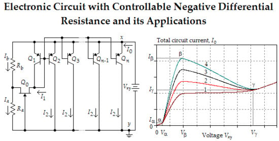
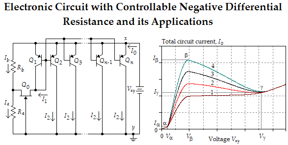
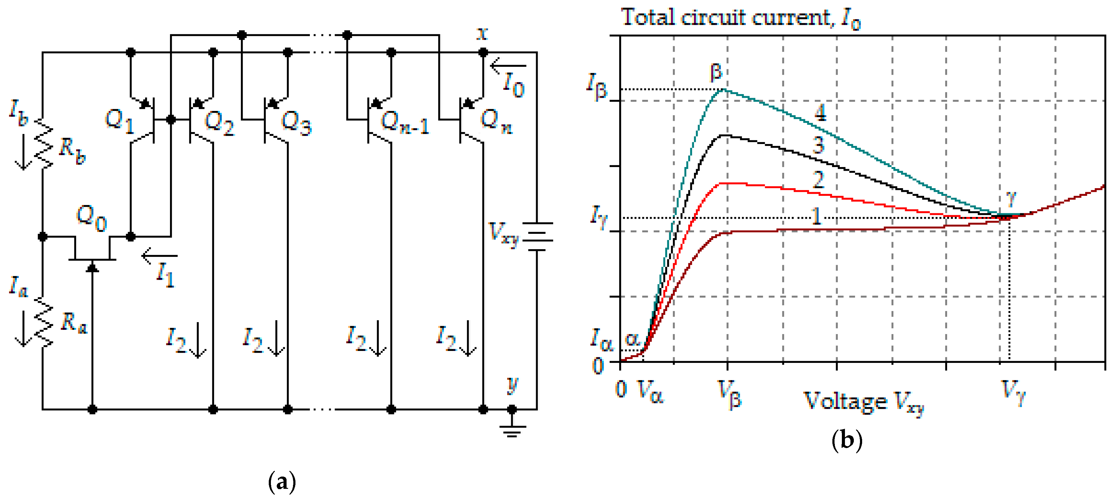
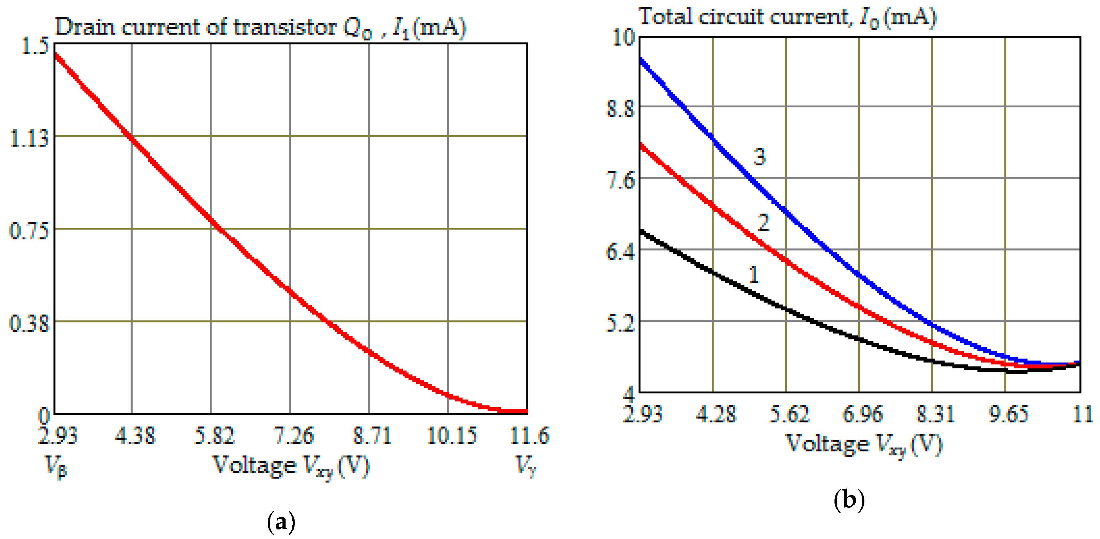
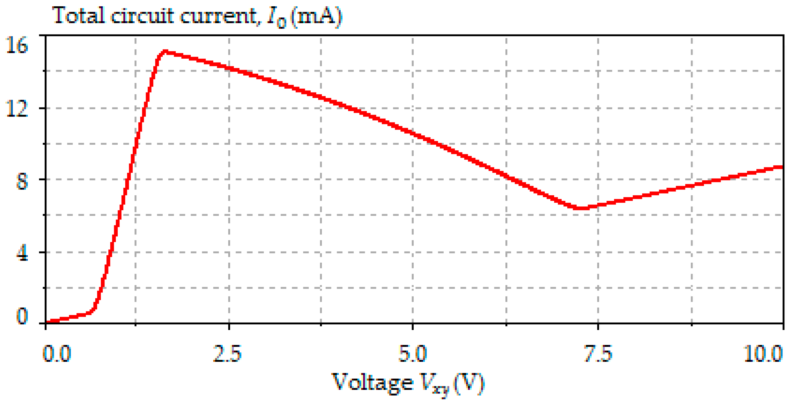
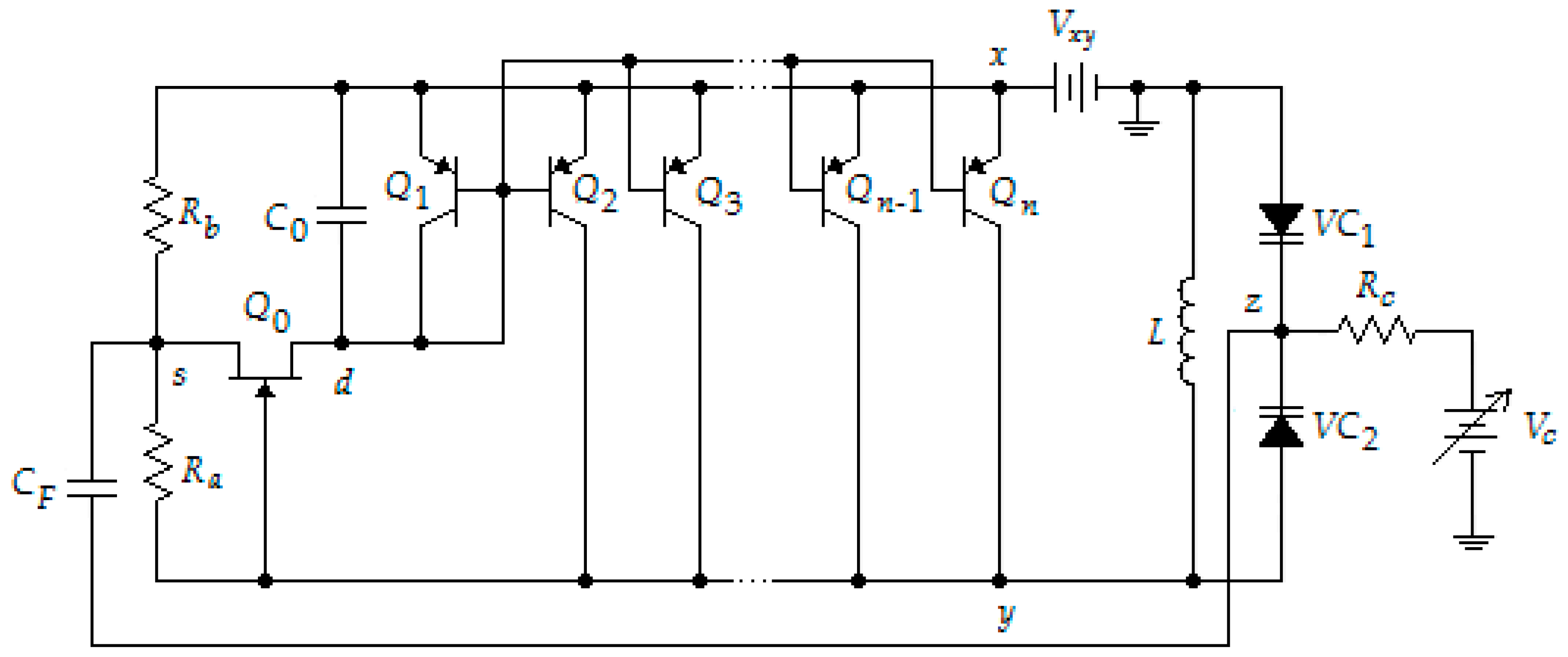
2. Circuit Operation

Figure 1a shows the proposed NDR circuit, which consists of two bias resistors R a and R b , a FET ( Q 0 ) and simple CM with n 1 outputs (collectors of transistors Q 2 , Q n ¯ ). We further assume that transistors Q 1 , Q n ¯ are matched. Figure 1b shows the current-voltage characteristics of the NDR circuit where the total current I 0 is a function of the power supply voltage V x y . The steepness of the current-voltage characteristic between points β and γ depends on the number of outputs of the CM. Curve 1 corresponds to the one output of the CM, i.e., only transistors Q 1 and Q 2 are used. In this particular case, the differential resistance between points β and γ is positive, and the circuit does not have an NDR region. When choosing the appropriate transistors, the circuit can have the NDR region even with one CM output.
As can be seen in Figure 1b, with an increase in the number of the CM outputs to two and further to four, the differential resistance becomes negative and the slope of the characteristic in the NDR region increases.
The current-voltage characteristics in Figure 1b include four regions, respectively, between points 0 and V α , V α and V β , V β and V γ , and V γ and . The NDR region is located between points V β and V γ .
Let’s look at the general principle of the circuit operation. When voltage V x y varies from 0 to V α , all transistors in the circuit are OFF. At the supply voltage V α , all transistors are turning ON, and, up to the voltage V β , the current I 1 rises, and the total current I 0 also increases. The current I 2 is a mirrored copy of I 1 , and it behaves like I 1 .When the supply voltage is V β , the current I 1 reaches a maximum, which also corresponds to the maximum of the total current I 0 . When the voltage V x y changes from V β to V γ , the current I 1 decreases due to an increase in the negative voltage between the gate and the source of the transistor Q 0 . At the same time, an increase in current I b does not cover this decrease in current I 1 . As a result, the total current I 0 decreases up to the voltage V γ , at which the voltage between the gate and the source of the transistor Q 0 reaches a pinch-off voltage and Q 0 is turning OFF, and, consequently, the transistors Q 1 , Q n ¯ also turning OFF. When the supply voltage is higher than V γ , the total current I 0 is entirely determined by the voltage V x y and the resistances of R a and R b . Therefore, in the interval ( V γ ,   ) differential resistance of the current-voltage characteristics is positive.
Let us determine the coordinates of points α, β, and γ. In the first region of the current-voltage characteristics, between points 0 and V α , all transistors are OFF, and the overall current depends on the resistor values R a and R b , and power supply voltage V x y .
I 0 = V x y R a + R b .
The threshold voltage V α is determined by applying Kirchhoff’s voltage law (KVL) equation to the circuit of Figure 1a when transistor Q 0 is turning ON and V D S 0 = 0 , where V D S 0 is the drain-source voltage of Q 0 .
V α = V E B + I a R a ,
where V E B is the emitter-base voltage of transistors ( Q 1 , Q n ¯ ) and I a is the current through resistor R a . Since at voltage V α the current I a is equal to I 0 , then Equation (2) transforms to the following form:
V α = V E B ( R a + R b ) R b .
Combining (1) and (3), we obtain:
I α = V E B R b .
When voltage V x y a little exceeds V α transistors Q 1 , Q n ¯ are turning ON, and transistor Q 0 starts to operate in the triode region where:
V D S 0 < V G S 0 + V P 0 ,
where V G S 0 and V P 0 are, respectively, the gate-source and pinch-off voltage of Q 0 .
By applying KVL from + V x y to ground, we get:
V x y = V E B + V D S 0 + I a R a .
From (6) we find current I a as follows:
I a = V x y V E B V D S 0 R a
As it follows from the circuit of Figure 1a:
I b = I a I 1 .
Substituting (7) to (8) gives:
I b = V x y V E B V D S 0 R a I 1 .
Applying KVL around the loop ( R b ,   Q 0 ,   Q 1 ) , we obtain:
I b R b + V D S 0 + V E B = 0 .
Substituting (9) into (10) and performing some mathematical transformations, we get:
V D S 0 = R b V x y R a + R b I 1 ( R a R b ) V E B .
The gate-source voltage of transistor Q 0 is given by:
V G S 0 = I a R a .
Voltage V G S 0 we obtain by combining (7), (11), and (12) and performing necessary transformations.
V G S 0 = R a V x y R a + R b I 1 ( R a R b ) .
Substituting V D S 0 from (11) to (7), we determine that:
I a = V x y R a + R b + I 1 R b R a + R b .
We find the current I 0 by applying Kirchhoff’s current law (KCL) to the node y in the circuit of Figure 1a.
I 0 = I a + ( n 1 ) I 2 .
By substitution of (14) into (15), we obtain general equation for the circuit total current.
I 0 = ( n 1 ) I 2 + I 1 R b R a + R b + V x y R a + R b .
Since the current I 2 is close to the reference current I 1 , we can assume that I 2 I 1 . In this case Equation (16) transforms into the following form:
I 0 I 1 ( n 1 + R b R a + R b ) + V x y R a + R b .
The slope of the current-voltage characteristics in the region of negative resistance is determined by the first derivative of the current I 0 with respect to the voltage V x y .
d I 0 d V x y ( n 1 + R b R a + R b ) d I 1 d V x y + 1 R a + R b .
As can be seen from (18), the slope is indeed proportional to the number of outputs of the current-mirror n. Therefore, by changing n, it is possible to reduce or increase the slope of the current-voltage characteristics between the voltage thresholds V β and V γ .
Substituting (11) and (13) into (5), we find that when transistor Q 0 operates in the triode mode, the following relationship holds between the supply voltage V x y and the voltages V E B and V P 0 :
V x y < V E B V P 0 .
When voltage V x y increases more, FET Q 0 reaches the saturation region where:
V D S 0 V G S 0 + V P 0 .
The threshold voltage V β is reached at the boundary between the triode and the saturation region of transistor Q 0 , i.e., when:
V D S 0 = V G S 0 + V P 0 .
Substituting (11) and (13) into (21), we obtain the threshold voltage V β .
V β = V E B V P 0 .
We determine the threshold current I β by substitution of (22) into (17).
I β I 1 ( n 1 + R b R a + R b ) + V E B V P 0 R a + R b .
As can be seen in Figure 1b, the slope of the current-voltage characteristics in the regions ( 0 ,   V α ) and ( V γ ,   ) is the same. It means that at the voltage threshold V γ the FET Q 0 is OFF and I 1 = 0 . Transistor Q 0 is turning OFF when V G S 0 = V P 0 . Substituting V P 0 instead of V G S 0 into (13) and solving the obtained equation with respect to V x y , we get:
V x y = V γ = ( 1 + R b R a ) V P 0 .
The threshold current I γ we find by substituting V x y from (24) into (1).
I γ = | V P 0 | R a .
As can be seen from (11), (13), (14), (16), (17), and (23), to calculate the currents and voltages related to the thresholds of the circuit current-voltage characteristics, it is necessary to know the current I 1 . Modeling the current I 1 depends on the type of FET Q 0 . Transistor Q 0 can be an N-channel JFET, metal-semiconductor field-effect transistor (MESFET), high-electron-mobility transistor (HEMT), or pseudomorphic high-electron-mobility transistor (PHEMT). In the voltage region ( V β , V γ ) transistor Q 0 operates in the saturation mode. Therefore, we should model the current I 1 for the case when Q 0 operates in the saturation mode.
As is well known, the operation of a JFET in the saturation mode is quite good described by the Shockley equation [23].
Substituting V G S 0 from (13) to the Shockley equation gives:
I 1 = I D S S ( 1 + A V x y + B I 1 V P 0 ) 2 ,
where I D S S is the saturation drain-source current at zero gate–source voltage, A and B are determined as follows:
A = R a / ( R a + R b ) , B = R a R b .
Solving (26) with respect to current I 1 , we obtain the following quadratic equation:
I D S S B 2 V P 0 2 I 1 2 + [ 2 I D S S ( 1 + A V x y V P 0 ) B V P 0 1 ] I 1 + I D S S ( 1 + A V x y V P 0 ) 2 = 0 .
Equation (27) has two positive roots. The acceptable root is the value of the current I 1 that is less than I D S S .
Figure 2a shows the dependence of the drain current I 1 versus power supply voltage V x y in the interval ( V β , V γ ) when BF245B is used as a JFET Q 0 and Positive-Negative-Positive (PNP) BJT transistors BFT92W are used in the CM. Assume that R a = 0.5   k Ω , R b = 2   k Ω , and n = 5 , i.e., the CM has four outputs. From the simulation program with integrated circuit emphasis (SPICE) model of the selected JFET transistor follows that V P 0 = 2.31   V and I D S S = 6   mA .
As can be seen in Figure 2a, in the NDR region the current I 1 changes from 1.47 mA to 0. Figure 2b shows the dependence of the total current I 0 versus voltage V x y in the NDR region when n = 4 (curve 1), n = 5 (curve 2), and n = 6 (curve 3).
The curves in Figure 2b were calculated using (17) and (27). As can be seen in Figure 2b, the total current I 0 increases by the same value with each increase in the number of the CM outputs. At the same time, the threshold voltage V γ shifts slightly to the right with increasing n .
Let us compare the calculated and simulated voltage and current thresholds for the circuit of Figure 1a for the same data as in Figure 2. From the interactive SPICE simulation of transistor BFT92W operation with the help of Multisim (ed. 14.1) follows that V E B = 0.52   V (at threshold α) and V E B = 0.62   V (at threshold β). The results of calculations and SPICE simulations are shown in Table 1.
As can be seen in Table 1, the absolute relative error for the calculated voltage thresholds of the NDR region does not exceed 5% and for current thresholds slightly exceed 2.5%. Such a high accuracy of calculating voltage and current thresholds testifies on the adequacy of the derived mathematical equations.
Let us now consider the case when Q 0 is a GaAs transistor, i.e., MESFET, HEMT, or PHEMT. We model the current of Q 0 by the Statz nonlinear model, which has a high accuracy in the approximation of the drain current [24].
Substituting V D S 0 and V G S 0 from (11) and (13) to the Statz model [24,25], we get the following nonlinear equations in respect to the drain current I 1 :
δ ( A V x y + B I 1 + V P 0 ) 2 1 Δ ( A V x y + B I 1 + V P 0 ) [ 1 + λ ( C V x y B I 1 V E B ) ] { 1 [ 1 α ( C V x y B I 1 V E B ) / 3 ] 3 } I 1 = 0 , for   0 < C V x y B I 1 V E B < 3 / α ,
δ ( A V x y + B I 1 + V P 0 ) 2 1 Δ ( A V x y + B I 1 + V P 0 ) [ 1 + λ ( C V x y B I 1 V E B ) ] I 1 = 0 ,   for   C V x y B I 1 V E B 3 / α ,
where α is the current saturation parameter, δ is the transistor transconductance, Δ is the doping profile parameter, λ is the channel length modulation coefficient, and C is determined as follows:
C = R b / ( R a + R b ) .
Let us again compare the calculated and simulated voltage and current thresholds for the circuit of Figure 1a when a low noise PHEMT ATF-33143 is used as transistor Q 0 and the same PNP transistors BFT92W are used in the CM. From the SPICE model of ATF-33143 [26] follows that α = 4   [ 1 / V ] , δ = 0.48   [ A / V 2 ] , Δ = 0.8 , λ = 0.09   [ 1 / V ] , and V P 0 = 0.95   [ V ] . The other circuit parameters have the same values as in the previous example.
To obtain the calculated values of the voltage and current thresholds, we solve Equations (28) and (29) and use Equations (3), (4), and (22)–(25). The results of calculations and SPICE simulations with the help of Multisim (ed. 14.1) are shown in Table 2.
As can be seen in Table 2, a good agreement exists between the theoretical and simulated values of the current and voltage thresholds, which proves the validity of the derived equations.

3. Circuit Applications

3.1. LC Oscillator

Oscillators are one of the main elements in modern communication, control, and navigation systems. Modern oscillators can be divided into two classes, namely oscillators with negative input impedance and oscillators with NDR. A distinctive feature of the first-class oscillators is the presence of a negative real part in the input impedance. Examples of such oscillators are numerous Colpitts, Clapp, Hartley oscillator circuits, and their modifications [27,28,29,30], as well as cross-coupled CMOS oscillators [31,32,33,34]. The second class of microwave oscillators supposes to use a tunnel diode or a Gunn diode [35,36], which have an NDR region in the N-type current-voltage characteristics. The location of the operating point in the NDR region leads to the creation of a negative resistance induced into the contour of the LC tank to compensate for its losses. The circuit of Figure 1a can also be used for designing an LC oscillator because it has an NDR region.
Figure 3 shows an LC oscillator on the base of the proposed NDR circuit. The oscillator tank circuit consists of an RF coil L and two series-connected capacitors C 1 and C 2 . Small capacitor C F is a feedback capacitor allowing to speed-up the oscillator start-up. Large capacitor C 0 reduces the noise level significantly at the nodes y, z, d, and s of the oscillator. This allows increasing the slope of the noise skirt around the fundamental harmonic, which in-turn reduces the oscillator phase noise.

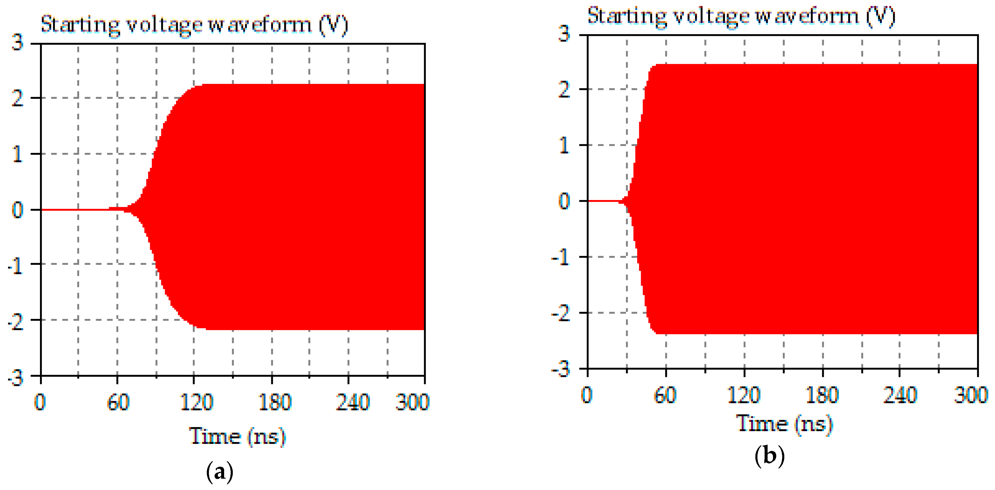
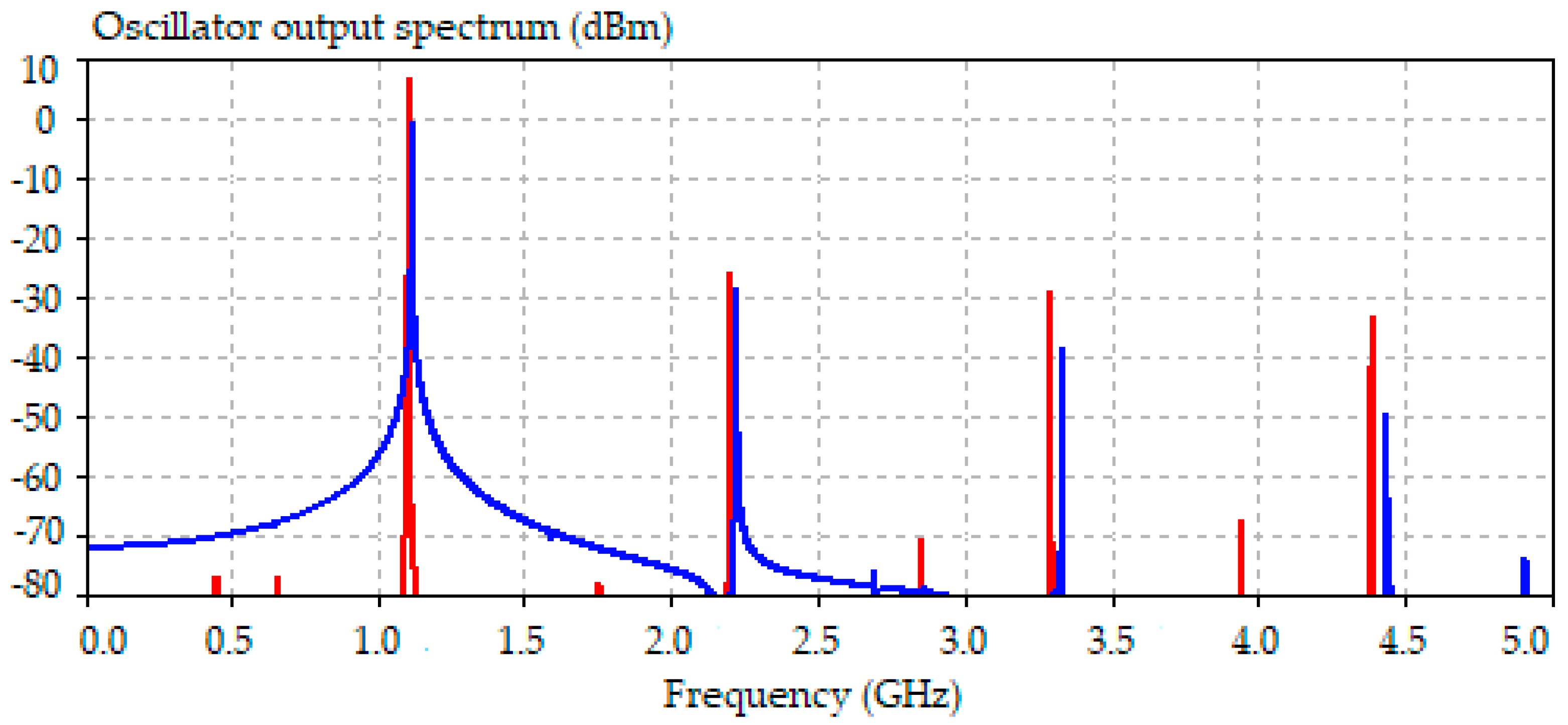
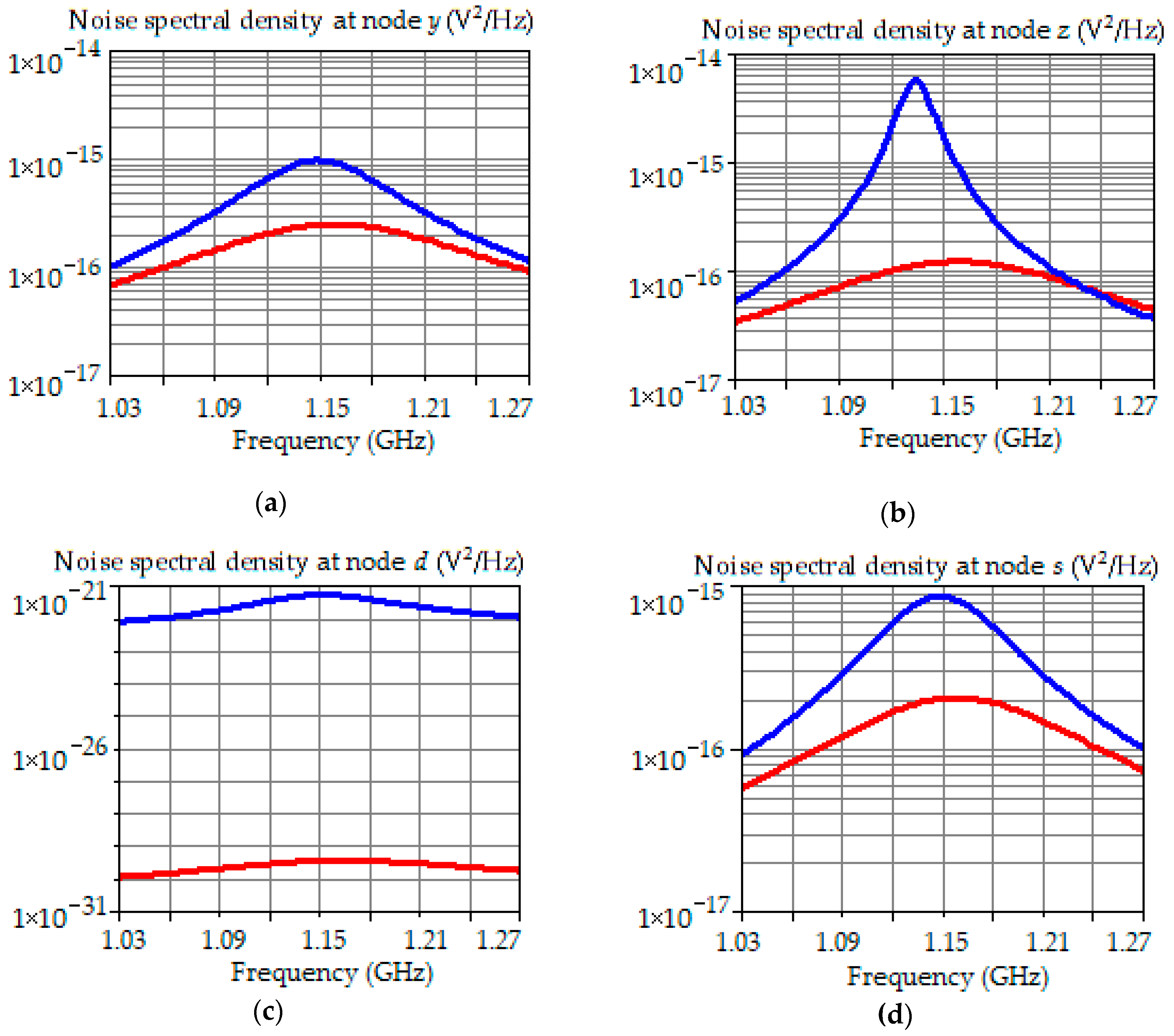
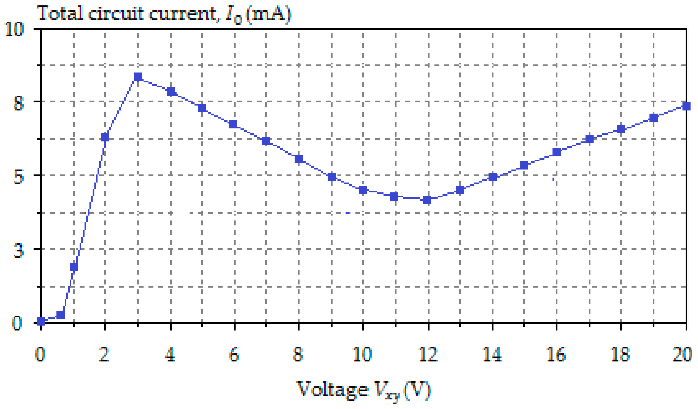
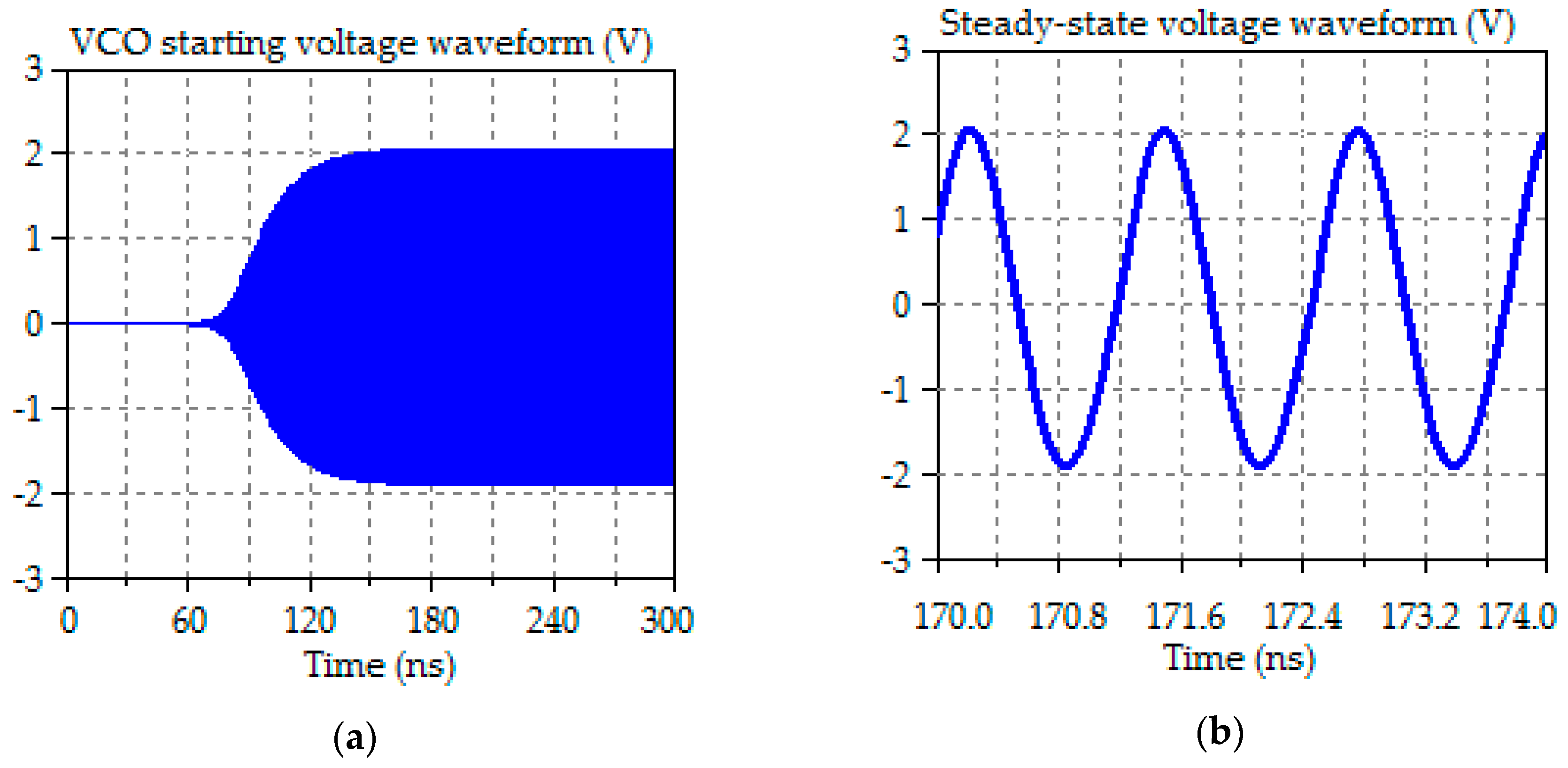
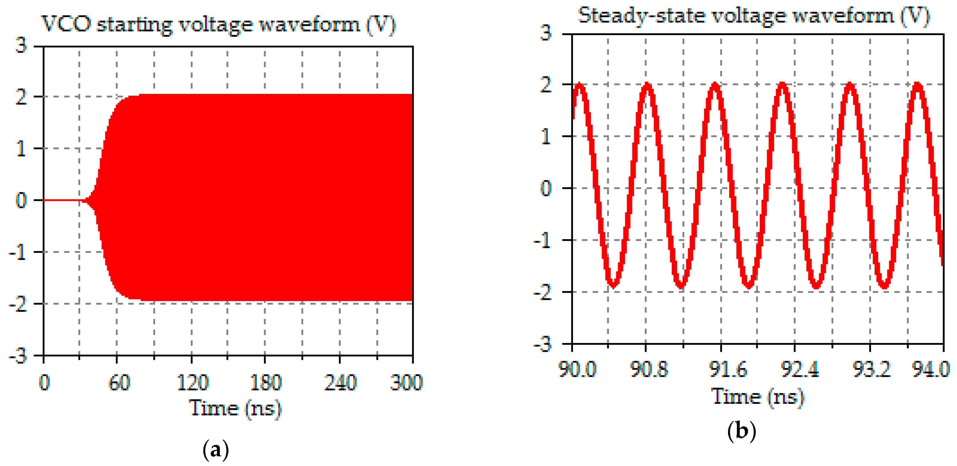
3.1.1. Simulation Results

Let us perform a SPICE simulation of the proposed oscillator circuit with the help of Multisim (ed. 14.1). Assume that n = 3 , R a = 0.15   k Ω , R b = 1   k Ω , transistor Q 0 is a PHEMT ATF-33143, and all transistors in the CM are BFT92W. Figure 4 shows the simulated current-voltage characteristics. As can be seen in Figure 4, the NDR region has the following voltage and current thresholds: V β = 1.58   V , I β = 15   mA , V γ = 7.26   V , and I γ = 6.33   mA . We set the operating point at V ¯ x y = 3.75   V and I ¯ 0 = 12.5   mA .
The selected circuit components have the following values: L = 5   nH , C 0 = 10   μ F , and C 1 = C 2 = 5   pF . Figure 5 shows the oscillator starting voltage waveforms at the output node y for different values of the feedback capacitor C F . The frequency of oscillations is 1.096 GHz. We can observe from Figure 5, that the oscillations reach the steady-state amplitude of 2.2 V at t = 130   ns and 2.4 V at t = 55   ns when C F = 5   pF and C F = 10   pF , respectively. Thus, an increase in the capacitance C F leads to a significant reduction in the self-excitation time of the oscillator and an increase in the amplitude of the steady-state oscillations.
Figure 6 shows the amplitude spectrum of the oscillated voltage for C 0 = 1   nF and C F = 5   pF (blue line) and C 0 = 10   μ F and C F = 10   pF (red line). As can be seen from comparison of two spectrums in Figure 6, the noise skirt of the fundamental harmonic at the level of -80 dBm is significantly narrower for larger values of capacitances C 0 and C F . Moreover, the total harmonic distortion (THD) is 3.3% for C 0 = 10   μ F and C F = 10   pF and 3.7% for C 0 = 1   nF and C F = 5   pF , i.e., larger capacitances C 0 and C F provide a smaller level of THD.
The decrease in the noise level of the oscillator output voltage in Figure 6 is explained by the fact that with an increase in the capacitances C 0 and C F , the simulated spectral density of noise decreases significantly at the nodes y, z, d, and s of the oscillator circuit as shown in Figure 7. As can be seen in Figure 7c, the most substantial decrease in noise spectral density occurs at the drain of transistor Q 0 , i.e., just where there is a large capacitance C 0 . This observation confirms a similar conclusion concerning the effect of capacitance on noise in CMOS LC oscillators [37].

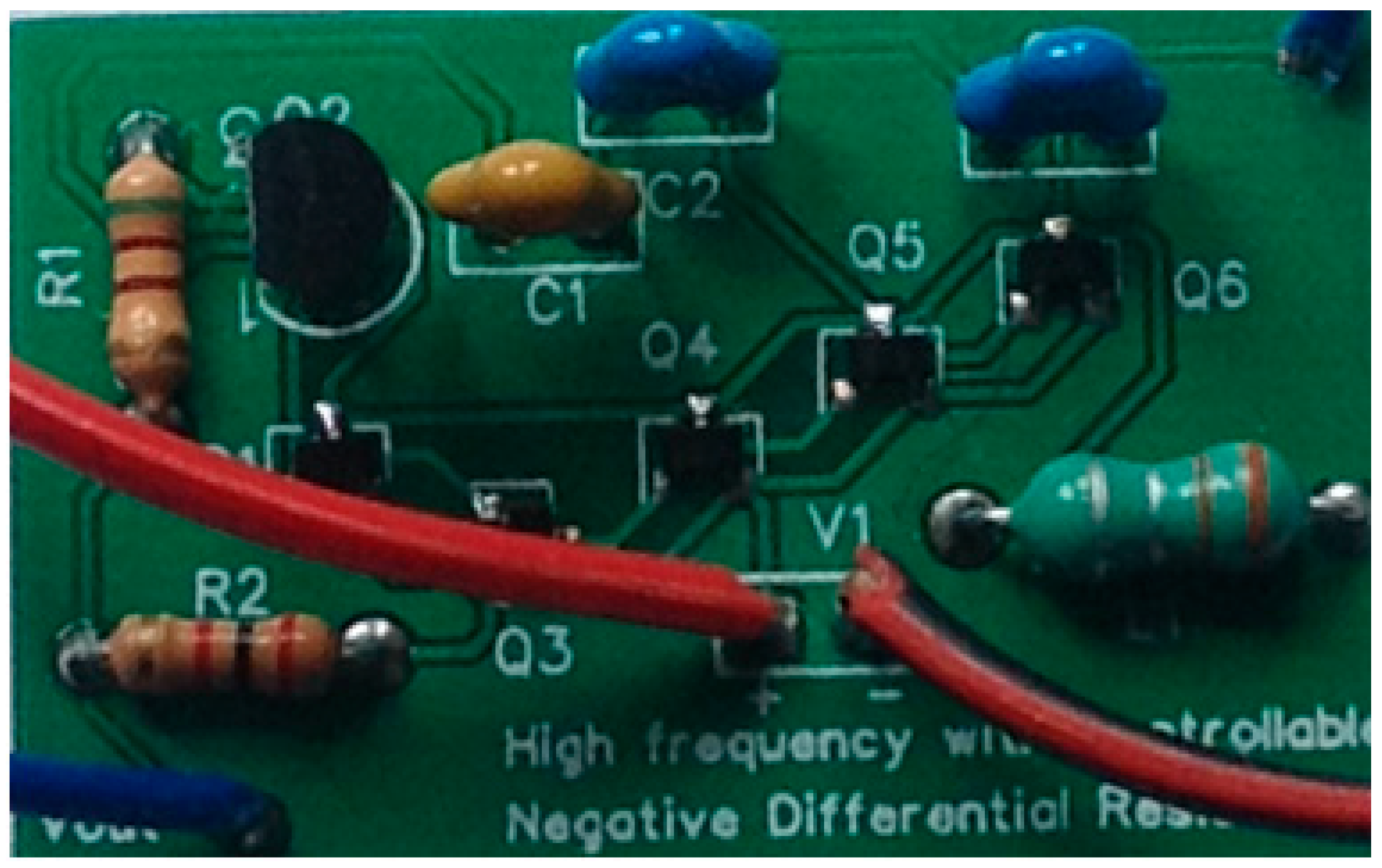
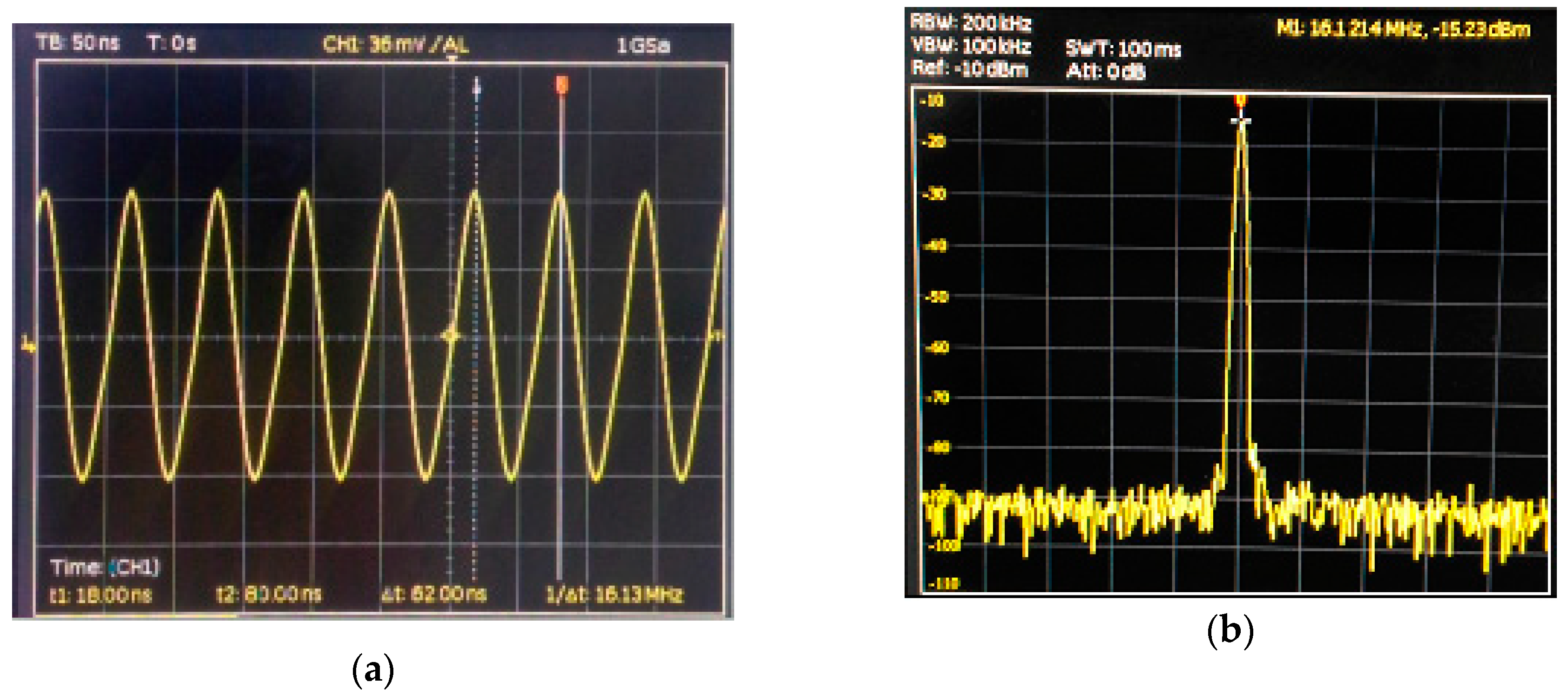
3.1.2. Oscillator Prototype Implementation

The oscillator circuit of Figure 3 was implemented using a JFET BF245B (NXP Semiconductors, Eindhoven, Netherlands) as transistor Q 0 and five transistors BFT92W (NXP Semiconductors, Eindhoven, Netherlands) in the CM, i.e., n = 5 . We selected the following component values: R a = 0.5   k Ω , R b = 2   k Ω , C 1 = C 2 = 82   pF , C F = 2.2   pF , C 0 = 0 , and L = 330   nH .
Figure 8 shows the printed circuit board (PCB) assembly of the implemented NDR oscillator.
Figure 9 shows the measured current-voltage characteristics of the implemented NDR oscillator. The measured values of the threshold voltages in the NDR region are V β * = 3   V and V γ * = 12   V . The calculation of the theoretical voltage thresholds by Equations (22) and (24) gives V β = 2.93   V and V γ = 11.55   V . As can be seen, there is a perfect agreement between the measured and theoretical results. The dc operating point has the following coordinates: V ¯ x y = 5.2   V and I ¯ 0 = 7.6   mA .
Figure 10 shows the photographs of the output voltage (a) and output power spectrum (b) of the implemented oscillator. We used the HMO1002 oscilloscope (Rohde & Swartz, Munich, Germany) and the HMS3000 spectrum analyzer (Rohde & Swartz, Munich, Germany) to measure the oscillator’s output voltage in the time and frequency domain. To connect the oscillator output to oscilloscope and spectrum analyzer, we used, respectively, RF probes HZ154 (Rohde & Swartz, Munich, Germany) and P-20A (Auburn Technology Corporation, Wichita, Kansas, USA) with 20 dB attenuation. We can see from Figure 10 that the frequency and the peak-to-peak amplitude of oscillations are 16.1 MHz and 4.12 V, respectively. We can also observe in Figure 10b that the noise-floor power level is more than 75 dB below the fundamental harmonic power.

3.2. LC Voltage Controlled Oscillator

Voltage-controlled oscillators are fundamental building units in modern phase-locked loop synthesizers used in communication and navigation transceivers [38,39,40]. The NDR circuit of Figure 1a can also be used to design an LC VCO. Figure 11 shows the proposed LC VCO with a controllable slope of the NDR region. The varactor diodes V C 1 and V C 2 replace the capacitors C 1 and C 2 in the circuit of Figure 3. The control voltage V c is applied to cathodes of varactor diodes V C 1 and V C 2 providing a frequency tuning of the VCO. Resistor R c isolates the variable power supply from the VCO tank circuit.
The SPICE simulation of the VCO circuit with the help of Multisim (ed. 14.1) was conducted using varactor diodes ZC820 (Zetex) and the same transistors, inductor L , and resistors R a and R b as in Section 3.1.1. We set the VCO circuit elements C 0 , C F , and R c to 10   μ F , 10   pF and 10   k Ω , respectively. The control voltage V c was varied from 1 to 25 V. Figure 12 and Figure 13 show the VCO starting voltage waveform (a) and steady-state voltage waveform (b) when V c = 1   V and V c = 25   V , respectively. The oscillation frequency varied from 775 MHz (at V c = 1   V ) to 1.375 GHz (at V c = 25   V ). The THD is 4.6% at V c = 1   V and 3.8% at V c = 25   V .
From a comparison of voltage starting waveforms in Figure 12a and Figure 13a, we can observe that voltage oscillations reach the steady-state mode at 160 ns and 80 ns, respectively. In the steady state operation mode, the voltage amplitude is around 2 V over the entire control voltage range.
Figure 14 shows the tuning characteristic of the VCO. As can be seen in Figure 14, the simulated VCO covers a wide frequency range. The ratio of the maximum VCO frequency to minimum exceeds 1.75.

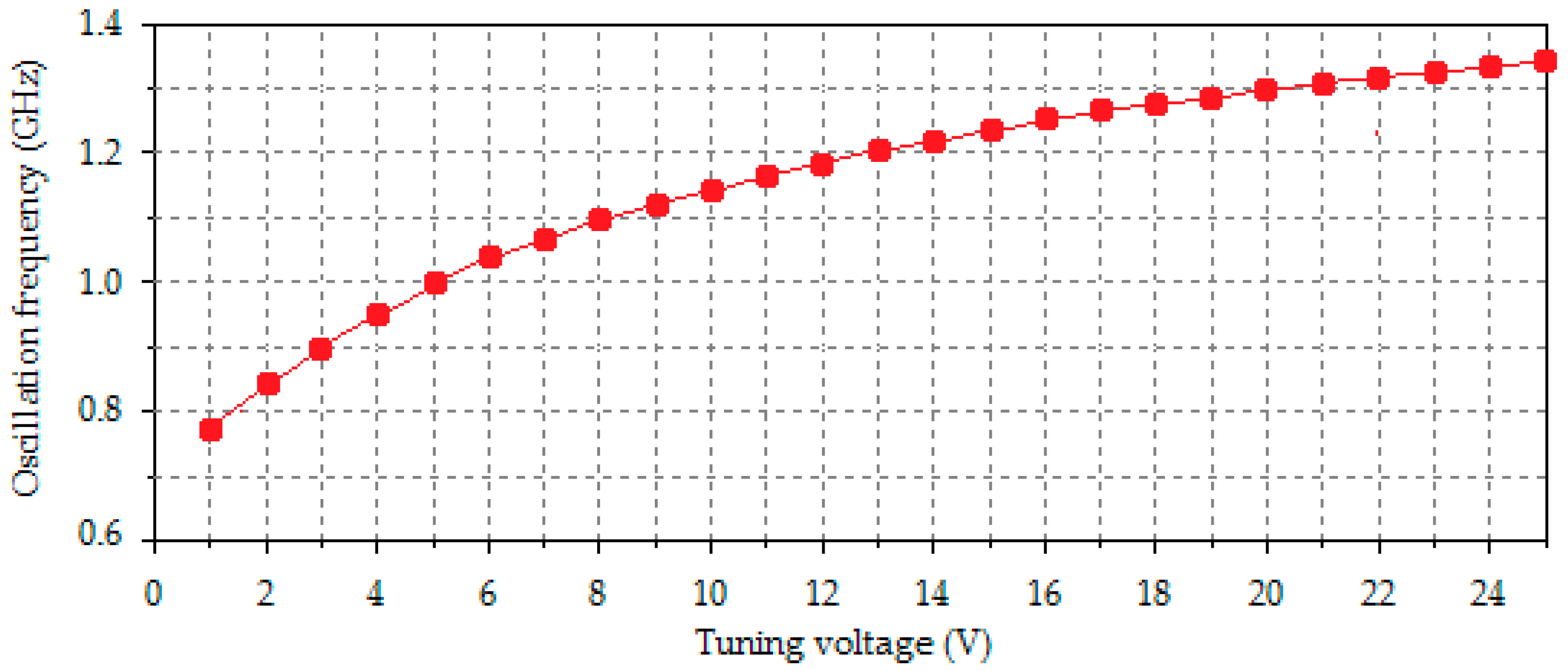
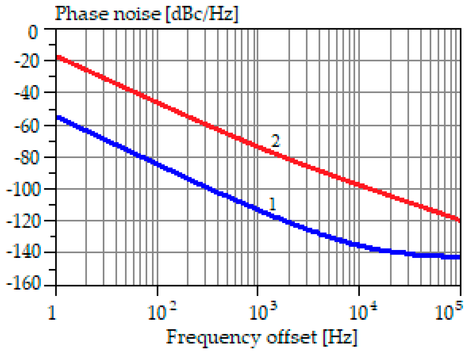
LC Voltage-Controlled Oscillator Performance

Let us compare the overall performance of the proposed NDR VCO with state of the art VCOs. The conventional FOM is used to evaluate the overall performance of the designed VCO, which includes phase noise at a particular frequency offset from the carrier P N ( Δ f ) , power dissipation P d , and the ratio of the carrier frequency f c to the frequency offset Δ f for comparing VCOs operating at different frequencies [41,42].
F O M = P N ( Δ f ) 20 log ( f c Δ f ) + 10 log ( P d 1   mW ) .
Table 3 presents the part numbers of the VCO elements. In the simulation, we used the VCO circuit of Figure 11 when n = 2. The simulated values of the NDR threshold voltages are as follows: V β = 2.84   V and V γ = 20.7   V . The calculated thresholds are V β = 2.84   V and V γ = 20.7   V . The selected DC operating point has the following coordinates: V ¯ x y = 6.5   V and I ¯ 0 = 8.5   mA . Thus, the VCO power dissipation is 55.25 mW. The control voltage V c applied to the cathodes of the SMV1104-34 varactors varied from 2 V to 6 V. The frequency tuning range is from 1.225 GHz to 1.620 GHz. Figure 15 shows the dependence of the VCO phase noise versus Δ f when V c = 2   V . As can be seen in Figure 15, the use of large C 0 reduces phase noise for more than 20 dB in all range of offset frequencies. The low level of the phase noise is also due to the use of a high-Q coil L [43]. In the tuning VCO range, the inductor quality factor is varied from 50 to 60.
Table 4 shows a comparison of the designed VCO with the VCOs in recently published studies in terms of the FOM (30). As can be seen in Table 4, the designed NDR VCO has one of the best FOM. It should be noted that all previously published VCOs in Table 4, except [58,59], fabricated in CMOS or BiCMOS technologies.
Oscillators manufactured using MESFET, HEMT, and PHEMT have significantly lower FOM values due to substantially higher power consumption [58,59]. However, as follows from Table 4, the proposed NDR VCO can even compete with the best CMOS oscillators due to the low level of phase noise and despite the significantly higher power consumption.

4. Discussion and Conclusions

There is a large number of electronic circuits [1,2,3,4,5,6,7,8,9,10,11,12,13,14,15,16,17,18,19,20,21,22], in which the current-voltage characteristics have an NDR region. The basis of these circuits is formed by various combinations of BJT and FET. Conventionally, the circuits with NDR can be classified into the following groups: circuits with MOS transistors [7,8,16,17,18,21], circuits with BJT transistors [10,14], circuits with BJT and JFET [11,12,13,14,15], circuits with JFET and MOS transistors [12,22], circuits with BJT and MOS transistors [9,20], and circuits with BJT and HBT [19]. It should be noted that in the known NDR devices and circuits it is practically impossible to change the angle of inclination of the current-voltage characteristics in the area of negative resistance. Therefore, it is not possible to increase the NDR of the device or circuit without changing the type or the size of the transistors.
This paper proposes a new NDR circuit based on the connection of a FET and a BJT simple current mirror with multiple outputs. A JFET, MESFET, HEMT, or PHEMT can be used as a FET. A distinctive feature of this circuit is the ability to control the NDR without changing the types or the size of transistors. This feature is based on the property of a simple current mirror to increase the current gain due to the parallel connection of transistors at the output of the mirror [59]. In the proposed circuit, the current-voltage characteristics are of the N-type with three threshold voltages. General mathematical equations for calculating the threshold voltages and currents have been derived. Since the threshold current related to the beginning of the NDR region depends on the FET drain current, a mathematical modeling of this current has been performed for a JFET and a gallium-arsenide FET, such as MESFET, HEMT, or PHEMT. A comparison of the calculated voltage and current thresholds with the SPICE simulations showed perfect convergence as for the case of using a JFET as well as for PHEMT, which was modeled by the Statz nonlinear model. The latter indicates the adequacy of mathematical expressions derived for the calculation of current and voltage thresholds.
The proposed NDR circuit can be used to design various oscillators. By connecting a parallel LC tank to the output of the proposed NDR circuit, one can get a sinusoidal oscillator, which can operate in different frequency bands. When using an ultra-high frequency JFET, the maximum frequency is limited to several hundred MHz. When using a gallium-arsenide transistor such as MESFET, HEMT, or PHEMT, the maximum oscillation frequency lies in the region of several GHz. Self-excitation of the oscillator by the proposed NDR circuit depends on the magnitude of the negative resistance introduced into the parallel LC tank circuit. If the value of the introduced negative resistance is sufficient to compensate for losses in the tank circuit, then the amplitude of oscillations increases and reaches a steady-state value. However, if the magnitude of the introduced negative resistance is insufficient, the oscillator does not self-excite. In any other NDR oscillator, in this case, it is necessary to change the transistors or their sizes for increasing negative resistance. However, in the proposed NDR circuit, it is enough to add one or more transistors in the current mirror as shown in Figure 1a and in this case, according to formula (18), the NDR will increase, and hence the absolute value of the negative resistance introduced into the tank circuit will also increase. Then the oscillator will oscillate. A SPICE simulation of the LC oscillator with a PHEMT and a BJT current-mirror at the frequency of 1.096 GHz showed that the generated signal has a low level of distortion, as well as a low noise level when using additional capacitances in the positive feedback circuit and between the drain of the PHEMT and ground. The implemented LC oscillator prototype operating in the high-frequency band has confirmed theoretical results. The proposed NDR circuit can also be used to design a VCO. Depending on the transistors used, such VCO can operate in different frequency bands, ranging from high-frequencies and up to microwaves. Thus, the simulated VCO circuit with PHEMT covers the frequency range from 775 MHz to 1.375 GHz, i.e., the frequency overlap ratio is higher than 1.75. Moreover, the amplitude of oscillation is about 2 V and practically does not change in the whole range of tunable frequencies. A comparison of the performance characteristics of the designed VCO with VCOs in previously published studies has shown that it is about 20 dB more efficient than the HEMT VCOs and is not inferior to the best CMOS VCOs.
The proposed NDR circuit can also be used in laboratory works in the electronics departments of universities to study the properties of negative resistance, to model various oscillators and to analyze the conditions for self-excitation of oscillators.
Our future work will include an analysis of the use of various bipolar and MOS current mirrors instead of the simple current mirror in the proposed NDR circuit.

Author Contributions

This article presents the collective work of all authors. The first two authors (V.U. and A.R.) jointly participated in the conceptualization of the problem, development of mathematical models, simulation of the developed circuits, numerical calculations, and writing the article. The third author (H.O.) developed a printed circuit board of the oscillator prototype, soldered electronic components, and made the necessary measurements.

Funding

This research received no external funding.

Conflicts of Interest

The authors declare no conflict of interest.

Abbreviations

The following abbreviations exist in the manuscript:
BJTBipolar junction transistor
CMCurrent mirror
CMOSComplementary metal-oxide-semiconductor
FETField-effect transistor
FOMFigure of merit
HBTHeterojunction bipolar transistor
HEMTHigh-electron-mobility transistor
JFETJunction gate field-effect transistor
KCLKirchhoff’s current law
KVLKirchhoff’s voltage law
MESFETMetal-semiconductor field-effect transistor
MOSMetal-oxide-semiconductor
MOSFETMetal-oxide-semiconductor field-effect transistor
NDRNegative differential resistance
NENSN-channel enhancement mode with load operated at saturation
PCBPrinted circuit board
PHEMTPseudomorphic high-electron-mobility transistor
PNPPositive-negative-positive
RFRadio frequency
SPICESimulation program with integrated circuit emphasis
THDTotal harmonic distortion
VCOVoltage controlled oscillator

References

  1. Tseng, P.; Chen, C.H.; Hsu, S.A.; Hsueh, W.J. Large negative differential resistance in graphene nanoribbon superlattices. Phys. Lett. A 2018, 382, 1427–1431. [Google Scholar] [CrossRef]
  2. Hwu, R.J.; Djuandi, A.; Lee, S.C. Negative differential resistance (NDR) frequency conversion with gain. IEEE Trans. Microw. Theory Tech. 1993, 41, 890–893. [Google Scholar] [CrossRef] [Green Version]
  3. Liang, D.S.; Gan, K.J. New D-Type Flip-Flop Design using negative differential resistance circuits. In Proceedings of the 4th IEEE International Symposium on Electronic Design, Test and Applications, Hong Kong, China, 23–25 January 2008; pp. 1–8. [Google Scholar]
  4. Chen, S.L.; Griffin, P.B.; Plummer, J.D. Negative differential resistance circuit design and memory applications. IEEE Trans. Electron Devices 2009, 56, 634–640. [Google Scholar] [CrossRef]
  5. Wang, S.; Pan, A.; Grezes, C.; Amiri, P.K.; Wang, K.L.; Chui, C.O.; Gupta, P. Leveraging nMOS negative differential resistance for low power, high-reliability magnetic memory. IEEE Trans. Electron Devices 2017, 64, 4084–4090. [Google Scholar] [CrossRef]
  6. Wu, Y.; Farmer, D.B.; Zhu, W.; Han, S.J.; Dimitrakopoulos, C.D.; Bol, A.A. Three-terminal graphene negative differential resistance devices. ACS Nano 2012, 6, 2610–2616. [Google Scholar] [CrossRef]
  7. Gan, K.J.; Hsiao, C.C.; Tsai, C.S.; Chen, Y.H.; Wane, S.Y.; Kuo, S.H. A novel voltage-controlled oscillator design by MOS-NDR devices and circuits. In Proceedings of the Fifth International Workshop on System-on-Chip for Real-Time Applications, Banff, AB, Canada, 20–24 July 2005; pp. 372–375. [Google Scholar]
  8. Tsai, C.S.; Hsiao, C.C.; Gan, K.J.; Wu, J.M.; Hsieh, M.Y.; Liao, C.C. An Oscillator Design Based on MOS-NDR Inverter. In Proceedings of the International Conference on Systems and Signals, Kaohsiung, Taiwan, 28–29 April 2005; pp. 1–5. [Google Scholar]
  9. Semenov, A. Mathematical model of the microelectronic oscillator based on the BJT-MOSFET structure with negative differential resistance. In Proceedings of the 2017 IEEE 37th International Conference on Electronics and Nanotechnology (ELNANO), Kiev, Ukraine, 18–20 April 2017; pp. 146–151. [Google Scholar]
  10. Gan, K.J.; Chun, K.Y.; Yeh, W.K.; Chen, Y.H.; Wang, W.S. Design of dynamic frequency divider using negative differential resistance circuit. Int. J. Recent Innov. Trends Comput. Commun. 2015, 3, 5224–5228. [Google Scholar]
  11. Stanley, I.W.; Ager, D.J. Two-terminal negative dynamic resistance. Electronic Lett. 1970, 6, 1–2. [Google Scholar] [CrossRef]
  12. Ulansky, V.V.; Ben Suleiman, S.F. Negative differential resistance based voltage-controlled oscillator for VHF band. In Proceedings of the 2013 IEEE International Scientific Conference on Electronics and Nanotechnology, Kiev, Ukraine, 16–19 April 2013; pp. 80–84. [Google Scholar]
  13. Kumar, U. Simulation of a novel bipolar-FET type-S negative resistance circuit. Act. Passiv. Electron. Compon. 2003, 26, 129–132. [Google Scholar] [CrossRef]
  14. Chua, L.O.; Yu, J.; Yu, Y. Bipolar-JFET-MOSFET negative resistance devices. IEEE Trans. Circuits Syst. 1985, 32, 46–61. [Google Scholar] [CrossRef]
  15. Ulansky, V.V.; Ben Suleiman, S.F.; Elsherif, H.M.; Abusaid, M.F. Optimization of NDR VCOs for microwave applications. In Proceedings of the 2016 IEEE 36th International Conference on Electronics and Nanotechnology (ELNANO), Kyiv, Ukraine, 19–21 April 2016; pp. 353–357. [Google Scholar]
  16. Akarvardar, K.; Chen, S.; Vandersand, J.; Blalock, B.; Schrimpf, R.; Prothro, B. Four-gate transistor voltage-controlled negative differential resistance device and related circuit applications. In Proceedings of the 2006 IEEE International SOI Conference, Niagara Falls, NY, USA, 2–5 October 2006; pp. 1–6. [Google Scholar]
  17. Shin, S.; Kim, K.R. Multiple negative differential resistance devices with ultra-high peak-to-valley current ratio for practical multi-valued logic and memory applications. Jpn. J. Appl. Phys. 2015, 54, 1–7. [Google Scholar] [CrossRef]
  18. Shin, S.; Kim, K.R. Novel five-state latch using double-peak negative differential resistance and standard ternary inverter. Jpn. J. Appl. Phys. 2016, 55, 1–6. [Google Scholar] [CrossRef]
  19. Gan, K.J.; Tsai, C.S.; Liang, D.S. Design and characterization of the negative differential resistance circuits using the CMOS and BiCMOS process. Analog Integr. Circuits Signal Process. 2010, 62, 63–68. [Google Scholar] [CrossRef]
  20. Gan, K.J.; Tsai, C.S.; Liang, D.S.; Wen, C.M.; Chen, Y.H. Tri-valued memory circuit using MOS-BJT-NDR circuits fabricated by standard SiGe process. Jpn. J. Appl. Phys. 2006, 45, 1–4. [Google Scholar] [CrossRef]
  21. Wu, C.Y.; Lai, K.N. Integrated Λ-type differential negative resistance MOSFET device. IEEE J. Solid-State Circuits 1979, 14, 1094–1101. [Google Scholar]
  22. Ulansky, V. Low phase-noise HEMT microwave voltage-controlled oscillator. In Proceedings of the IEEE Microwaves, Radar and Remote Sensing Symposium (MRRS), Kiev, Ukraine, 25–27 August 2011; pp. 55–58. [Google Scholar]
  23. Jagger, R.C.; Blalock, T.N. Microelectronic Circuit Design, 2nd ed.; McGraw-Hill: New York, NY, USA, 2004; pp. 251–254. [Google Scholar]
  24. Statz, H.; Newman, P.; Smith, W.; Pucel, R.A.; Haus, H.A. GaAs FET device and circuit simulation in Spice. IEEE Trans. Electron Devices 1987, 34, 160–169. [Google Scholar] [CrossRef]
  25. Converting GaAs FET Models for Different Nonlinear Simulators. Available online: https://docplayer.net/21705870-California-eastern-laboratories-an1023-converting-gaas-fet-models-for-different-nonlinear-simulators.html (accessed on 2 April 2003).
  26. ATF-33143. Low Noise Pseudomorphic HEMT in a Surface Mount Plastic Package. Data Sheet. Available online: https://cdn.datasheetspdf.com/pdf-down/A/T/F/ATF-33143-AVAGO.pdf (accessed on 6 January 2006).
  27. Conan Zhan, J.H.; Maurice, K.; Duster, J.; Kornegay, K.V. Analysis and design of negative impedance LC oscillators using bipolar transistors. IEEE Trans. Circuits Syst. I Fundam. Theory Appl. 2003, 50, 1461–1464. [Google Scholar] [CrossRef]
  28. Ulansky, V.V.; Fituri, M.S.; Machalin, I.A. Mathematical modeling of voltage-controlled oscillators with the Colpitts and Clapp topology. Electron. Control Syst. 2009, 19, 82–90. [Google Scholar]
  29. Chung, C.; Chao, S. Robust Colpitts and Hartley oscillator design. In Proceedings of the 2014 IEEE International Frequency Control Symposium (FCS), Taipei, Taiwan, 19–24 May 2014; pp. 1–5. [Google Scholar]
  30. Ulansky, V.V.; Elsherif, H.M. A new method of designing UHF FET Colpitts oscillator. In Proceedings of the 2014 IEEE 34th International Scientific Conference on Electronics and Nanotechnology (ELNANO), Kyiv, Ukraine, 15–18 April 2014; pp. 388–392. [Google Scholar]
  31. Daliri, M.; Maymandi-Nejad, M. Analytical model for CMOS cross-coupled LC-tank oscillator. IET Circuits Devices Syst. 2014, 8, 1–5. [Google Scholar] [CrossRef]
  32. Hajimiri, A.; Lee, T.H. Design issues in CMOS differential LC oscillators. IEEE J. Solid-State Circuits 1999, 34, 717–724. [Google Scholar] [CrossRef] [Green Version]
  33. Hou, J.A.; Wang, Y.H. A 5 GHz differential Colpitts CMOS VCO using the bottom PMOS cross-coupled current source. IEEE Microw. Wirel. Compon. Lett. 2009, 19, 401–403. [Google Scholar]
  34. Grebennikov, A. RF and Microwave Transistor Oscillator Design; John Wiley & Sons Ltd.: Chichester, UK, 2007; 458p. [Google Scholar]
  35. Poole, C.; Darwazeh, I. Microwave Active Circuit Analysis and Design; Elsevier: Amsterdam, The Netherlands, 2016; 664p. [Google Scholar]
  36. Sze, S.M. Active Microwave Diodes in Modern Semiconductor Device Physics; Wiley: New York, NY, USA, 1997; pp. 343–407. [Google Scholar]
  37. Hegazi, E.; Sjoland, H.; Abidi, A.A. A filtering technique to lower LC oscillator phase noise. IEEE J. Solid-State Circuits 2001, 36, 1921–1930. [Google Scholar] [CrossRef] [Green Version]
  38. Bianchi, G. Phase-Locked Loop Synthesizer Simulation; McGraw-Hill: New York, NY, USA, 2005; pp. 64–78. [Google Scholar]
  39. Luong, H.C.; Leung, G.C.T. Low-Voltage CMOS RF Frequency Synthesizers; Cambridge University Press: Cambridge, UK, 2004; pp. 28–44. [Google Scholar]
  40. Leenaerts, D.; van der Tang, J. Circuit Design for RF Transceivers; Springer: Berlin, Germany, 2001; 323p. [Google Scholar]
  41. Kinget, P. Integrated GHz voltage-controlled oscillators. In Analog Circuit Design; Sansen, W., Huijsing, J., van de Plassche, R., Eds.; Springer: Berlin, Germany, 1999; pp. 353–381. [Google Scholar]
  42. Tiebout, M. Low Power VCO Design in CMOS; Springer: Berlin, Germany, 2006; 128p. [Google Scholar]
  43. Coilcraft. RF Inductor Comparison Tool. Q vs Frequency. Available online: https://www.coilcraft.com/apps/compare/compare_rf.cfm (accessed on 11 October 2018).
  44. Cai, H.L.; Yang, Y.; Qi, N. A 2.7-mW 1.36–1.86-GHz LC-VCO with a FOM of 202 dBc/Hz enabled by a 26%-size-reduced nano-particle-magnetic-enhanced inductor. IEEE Trans. Microw. Theory Tech. 2014, 62, 1221–1228. [Google Scholar] [CrossRef]
  45. Rout, P.K.; Nanda, U.K.; Acharya, D.P.; Panda, G. Design of LC VCO for optimal figure of merit performance using CMODE. In Proceedings of the 1st International Conference on Recent Advances in Information Technology (RAIT), Dhanbad, India, 15–17 March 2012; pp. 1–6. [Google Scholar]
  46. Kim, S.J.; Seo, D.I.; Kim, J.S. Compact CMOS LiT VCO achieving 198.6 dBc/Hz FoM. Electron. Lett. 2018, 54, 175–177. [Google Scholar] [CrossRef]
  47. Zailer, E.; Belostotski, L.; Plume, R. 8-GHz, 6.6-mW LC-VCO with small die area and FOM of 204 dBc/Hz at 1-MHz offset. IEEE Microw. Wirel. Compon. Lett. 2016, 26, 936–938. [Google Scholar] [CrossRef]
  48. Chung, T.W.; Huang, T.C.; Chung, S. A 2.7GHz 3.9mW mesh-BJT LC-VCO with −204dBc/Hz FOM in 65nm CMOS. In Proceedings of the IEEE Custom Integrated Circuits Conference, San Jose, CA, USA, 9–12 September 2012; pp. 1–6. [Google Scholar]
  49. Narayanan, A.T.; Kimura, K.; Deng, W. A pulse-driven LC-VCO with a figure-of-merit of −192dBc/Hz. In Proceedings of the 40th European Solid-State Circuits Conference (ESSCIRC), Venice Lido, Italy, 22–26 September 2014; pp. 1–5. [Google Scholar]
  50. Lin, Y.C.; Yeh, M.L.; Chang, C.C. A high figure-of-merit low phase noise 15-GHz CMOS VCO. J. Mar. Sci. Technol. 2013, 21, 82–86. [Google Scholar]
  51. Ghorbel, I.; Haddad, F.; Rahajandraibe, W. Optimization of voltage-controlled oscillator VCO using current-reuse technique. In Proceedings of the 26th International Conference on Microelectronics (ICM), Doha, Qatar, 14–17 December 2014; pp. 1–5. [Google Scholar]
  52. Bhat, M.V.; Jain, S.; Srivatsa, M.P. Design of low phase noise voltage-controlled oscillator for phase locked loop. In Proceedings of the International Conference on Microelectronic Devices, Circuits and Systems (ICMDCS), Vellore, India, 10–12 August 2017; pp. 1–5. [Google Scholar]
  53. Mirajkar, P.; Chand, J.; Aniruddhan, S.; Theertham, S. Low phase noise Ku-band VCO with optimal switched-capacitor bank design. IEEE Trans. Very Larg. Scale Integr. (VLSI) Syst. 2018, 26, 589–593. [Google Scholar] [CrossRef]
  54. Zuo, C.; der Spiegel, J.V.; Piazza, G. Dual-mode resonator and switchless reconfigurable oscillator based on piezoelectric AlN MEMS technology. IEEE Trans. Electron Devices 2011, 58, 3599–3603. [Google Scholar] [CrossRef]
  55. Rottava, R.E.; Camara Santes Junior, C.; Rangel de Sousa, F.; Nunes de Lima, R. Ultra-low-power 2.4 GHz Colpitts oscillator based on double feedback technique. In Proceedings of the IEEE International Symposium on Circuits and Systems, Beijing, China, 19–23 May 2013; pp. 1785–1788. [Google Scholar]
  56. Sachan, D.; Kumar, H.; Goswami, M.; Misra, P.K. A 2.4 GHz low power low phase-noise enhanced FOM VCO for RF applications using 180 nm CMOS technology. Wirel. Pers. Commun. 2018, 101, 391–403. [Google Scholar] [CrossRef]
  57. Thi Do, T.N.; Szhau Lai, S.; Horberg, M. A MMIC GaN HEMT voltage-controlled-oscillator with high tuning linearity and low phase noise. In Proceedings of the IEEE Compound Semiconductor Integrated Circuit Symposium (CSICS), New Orleans, LA, USA, 11–14 October 2015; pp. 1–4. [Google Scholar]
  58. Liu, H.; Zhu, X.; Boon, C.C. Design of ultra-low phase noise and high power integrated oscillator in 0.25µm GaN-on-SiC HEMT technology. IEEE Microw. Wirel. Compon. Lett. 2014, 24, 120–122. [Google Scholar] [CrossRef]
  59. Gray, P.R.; Hurst, P.J.; Lewis, S.H.; Meyer, R.G. Analysis and Design of Analog Integrated Circuits; John Wiley & Sons, Inc.: New York, NY, USA, 2001; 875p. [Google Scholar]
Figure 1. (a) Negative differential resistance circuit with multiple simple current mirror; (b) N-type current-voltage characteristics of the circuit.
Electronics 08 00409 g001
Figure 2. (a) Dependence of the drain current I 1 versus voltage V x y ; (b) Dependence of the total current I 0 versus voltage V x y in the negative differential resistance region when n = 4 (curve 1), n = 5 (curve 2), and n = 6 (curve 3).
Electronics 08 00409 g002
Figure 3. LC oscillator with NDR.
Electronics 08 00409 g003
Figure 4. Oscillator current-voltage characteristics.
Electronics 08 00409 g004
Figure 5. Oscillator start-up behavior at C F = 5   pF (a) and C F = 10   pF (b).
Electronics 08 00409 g005
Figure 6. Oscillator output spectrum when C 0 = 1   nF and C F = 5   pF (blue line) and C 0 = 10   μ F and C F = 10   pF (red line).
Electronics 08 00409 g006
Figure 7. Noise spectral density at nodes y (a), z (b), d (c), and s (d) when C 0 = 1   nF and C F = 5   pF (blue line) and C 0 = 10   μ F and C F = 10   pF (red line).
Electronics 08 00409 g007
Figure 8. Photograph of the NDR oscillator printed circuit board assembly.
Electronics 08 00409 g008
Figure 9. Measured current-voltage characteristics of the implemented NDR oscillator.
Electronics 08 00409 g009
Figure 10. (a) The oscillogram of the oscillator output voltage; (b) The measured spectrum of the oscillator output power with span of 20 MHz.
Electronics 08 00409 g010
Figure 11. LC voltage-controlled oscillator with NDR.
Electronics 08 00409 g011
Figure 12. (a) Voltage-controlled oscillators (VCO) starting voltage waveform when V c = 1   V ; (b) VCO steady-state voltage when V c = 1   V .
Electronics 08 00409 g012
Figure 13. (a) VCO starting voltage waveform when V c = 25   V ; (b) VCO steady-state voltage when V c = 25   V .
Electronics 08 00409 g013
Figure 14. VCO tuning characteristic.
Electronics 08 00409 g014
Figure 15. Phase noise versus offset frequency when C 0 = 1   μ F (curve 1) and C 0 = 1   nF (curve 2).
Electronics 08 00409 g015
Table 1. Calculated and simulated threshold voltages and currents with junction gate field-effect transistor (JFET).
ThresholdCalculated ValueSimulated ValueError %
Vα (V)0.650.62−4.8%
Iα (mA)0.260.287.1%
Vβ (V)2.932.89−1.4%
Iβ (mA)8.228.301%
Vγ (V)11.6011.05−5.0%
Iγ (mA)4.624.50−2.7%
Table 2. Calculated and simulated threshold voltages and currents with pseudomorphic high-electron-mobility transistor (PHEMT).
ThresholdCalculated ValueSimulated ValueError %
Vα (V)0.650.62−4.8%
Iα (mA)0.260.287.1%
Vβ (V)1.571.718.2%
Iβ (mA)7.186.92−3.8%
Vγ (V)4.754.73−0.4%
Iγ (mA)1.91.910.5%
Table 3. Part numbers used in the designed voltage-controlled oscillator.
Circuit ElementsPart Numbers
Transistor Q 0 NE722S01
Transistors Q 1 , Q n ¯ MRF5211LT1
Inductor L0201DS-3N3XJEU
Capacitor C 0 C1608X5R1E105K
Capacitor C F C0603C0G1E030C
VaractorsSMV1104-34
Resistor R a ERJ1GEJ471
Resistor R b ERJ2GEJ392
Table 4. Performance of designed VCO and some recently published VCOs.
VCOFrequency GHzFrequency Offset MHzPhase Noise dBc/HzPower Dissipation mWFOM dBc/Hz
[44]1.610.1−1212.7−202
[45]2.51−119.70.515−190.3
[46]11.581−112.626−198.6
[47]81−134.36.6−204
[48]2.70.1−121.33.9−204
[49]3.61−1242.05−192
[50]15.571−116.66−192.7
[51]2.41−1200.267−193.3
[52]2.41−135.66.17−195.3
[53]12.671−120.617.7−190
[54]1.941−15320−205.7
[55]2.383−132.71−190.7
[56]2.41−1242.86−187.25
[57]71−132198−185.9
[58]7.91−1351456−181.3
This work1.2250.1−141.155.25−205.4

