Article

A 5GS/s 8-bit ADC with Self-Calibration in 0.18 μm SiGe BiCMOS Technology

1
Institute of Microelectronics of Chinese Academy of Sciences, Beijing 100029, China
2
School of Microelectronics, University of Chinese Academy of Sciences, Beijing 100049, China
3
Graduate School, Airforce Engineering University, Xi’an 710051, China
*
Author to whom correspondence should be addressed.
Electronics 2019, 8(2), 253; https://doi.org/10.3390/electronics8020253
Submission received: 4 January 2019 / Revised: 18 February 2019 / Accepted: 20 February 2019 / Published: 25 February 2019
(This article belongs to the Section Microelectronics)

Abstract

:
A 5 GS/s 8-bit analog-to-digital converter (ADC) implemented in 0.18 μm SiGe BiCMOS technology has been demonstrated. The proposed ADC is based on two-channel time-interleaved architecture, and each sub-ADC employs a two-stage cascaded folding and interpolating topology of radix-4. An open loop track-and-hold amplifier with enhanced linearity is designed to meet the dynamic performance requirement. The on-chip self-calibration technique is introduced to compensate the interleaving mismatches between two sub-ADCs. Measurement results show that the spurious free dynamic range (SFDR) stays above 44.8 dB with a peak of 53.52 dB, and the effective number of bits (ENOB) is greater than 5.8 bit with a maximum of 6.97 bit up to 2.5 GS/s. The ADC exhibits a differential nonlinearity (DNL) of -0.31/+0.23 LSB (least significant bit) and an integral nonlinearity (INL) of -0.68/+0.68 LSB, respectively. The chip occupies an area of 3.9 × 3.6 mm2, consumes a total power of 2.8 W, and achieves a figure of merit (FoM) of 10 pJ/conversion step.

1. Introduction

High-speed ADCs with moderate resolution are in high demand for applications such as the radar receiver. Although the flash ADC is known as the simplest and fastest architecture, the resolution is limited since the number of comparators increases exponentially with the number of bits, resulting in unacceptable complexity [1,2,3]. In pipelined ADC, large latency is inevitable because of the multiple pipeline stages, and this is undesirable for swift response situations. As for successive approximation register (SAR) ADC, which has superior energy efficiency, its speed potential usually requires very advanced technology (e.g. 40 nm or even smaller) because of its primarily digital nature [4,5,6]. Moreover, the sampling rate of a single SAR ADC is still not very high, so the time-interleaved architecture is often preferred for overcoming the speed limitation. Also, the number of interleaving channels is generally large, which requires a complex calibration process. Evolved from flash and two-step topologies, the folding and interpolating (F&I) architecture has low complexity along with the advantage of high speed and low latency by enabling simultaneous operation of the coarse and fine quantization.
In addition to the design topology, the manufacturing process is also an important consideration for the ADC implementation. Currently, ADCs are predominantly designed in a CMOS process. In fact, compared with metal-oxide-semiconductor field-effect transistor (MOSFET), silicon-germanium (SiGe) heterojunction bipolar transistors (HBT) possess higher transit frequency and superior matching property [7]. In addition, due to its reliability in extreme environmental conditions and inherent tolerance to irradiation effects, it is suitable for special applications such as space exploration [8,9,10]. With the rapid development of semiconductor integrated circuits, BiCMOS technology can offer the synthesis of low power excellence of CMOS and low distortion capability of HBT [11,12], facilitating the design of high-performance ADCs. Besides, the 0.18 μm SiGe BiCMOS technology is cost efficient and beneficial for special applications in low-volume manufacturing. In general, according to application requirements and cost considerations, the F&I ADC based on SiGe BiCMOS technology is an attractive choice.
In this paper, a prototype of a two-channel time-interleaved 5 GS/s 8-bit F&I ADC fabricated in 0.18 μm SiGe BiCMOS technology has been demonstrated. An open loop track-and-hold amplifier with enhanced linearity is designed to meet the dynamic specifications. The two-stage cascaded folding and interpolating structure of radix-4 is adopted, which makes use of the inherent relationship between folding operation and quantization process to get the most significant bits (MSBs) in parallel with the LSBs digitization, eliminating the traditional coarse quantization stage and requiring less hardware overhead. The self-calibration module is embedded inside the chip and proven to be very effective in reducing the inter-channel mismatches.
The outline of this paper is organized as follows. Section 2 describes the system architecture of the ADC, Section 3 discusses the design details and critical considerations of the key blocks, and Section 4 presents the self-calibration technique. Measurement results are illustrated in Section 5, and the conclusion is drawn in Section 6.

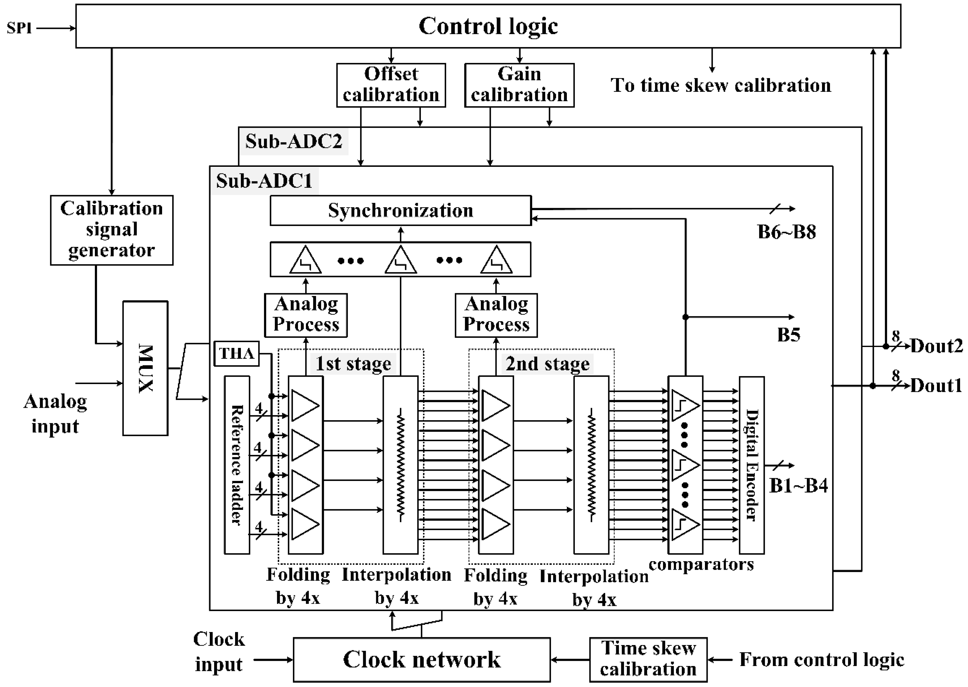
2. Proposed Architecture

The proposed ADC is based on two-channel time-interleaved architecture, and each sub-ADC adopts a two-stage cascaded folding and interpolating topology of radix-4, that is, both the folding factor (FF) and interpolating factor (IF) are equal to 4, as shown in Figure 1.
The ADC supports three operating modes, including a single-channel mode in which two identical sub-ADCs work in an interleaving manner with an equivalent sampling frequency of 5 GS/s, a dual-channel mode with two sub-ADCs that run independently at 2.5 GS/s, and a self-calibration mode for compensating the inter-channel mismatches automatically on-chip.
The control logic module can be accessed through the serial peripheral interface (SPI), offering flexible configurations of ADC operation. The calibration signal generator is integrated into the chip to provide special input signals for calibration purposes, which can effectively reduce the complexity of the calibration algorithm. The input signals or calibration signals can be routed to the ADC by a multiplexer (MUX) as needed.
The radix-4 folding and interpolating curves, as shown in Figure 2, have a natural mapping relationship with the quantization process of ADC, which is essentially binary (that is, radix-2) [13].
The F&I ADC folds the input signal into several sub-ranges with their zero-crossings corresponding to the reference voltages provided by the reference ladder. In order to reduce the number of folded amplifiers, an interpolating technique is introduced to add new folding curves that are uniformly distributed between adjacent folding curves. After two-stage folding and interpolating, 16 folding curves with FF of 16 are generated, including 256 equally spaced zero-crossings, which actually contain all the information needed for 8-bit quantization.
These 16 folding curves are fed into 16 comparators to translate the analog information into cyclical thermometer codes, which are then converted by the digital encoder to four LSBs (i.e. B1~B4) in binary format. Note that the F&I ADC extracts the information from the location of the comparison thresholds (i.e. zero-crossings) and not from the amplitude of the folding waveform. The quantization curve of the fifth bit resembles the folding curve (FF = 16) generated by the second stage interpolation circuit so that one of the comparison results from the comparators array can be directly used as B5. The situation is the same for B7, whose quantization curve is similar to the folding curve (FF = 4) from the first stage interpolation output. The number of quantization intervals for the eighth and sixth bits is 2 and 8, while the FF of the two-stage radix-4 folding curves is 4 or 16, so there is no direct correspondence between them. Fortunately, they have a common feature that is the power of 2; hence, the intermediate signals produced in the folding and interpolating operation can be transformed by the analog processing units to obtain the desired quantization curves, which are passed through the comparators to get B8 and B6. Besides, B5 is used to synchronize B6~B8. For traditional F&I ADC, the MSBs are resolved using a coarse flash stage in parallel with the LSBs digitization. In this design, the dedicated coarse flash channel is eliminated, and the MSBs are derived from the intermediate signals of the folding process [13].

3. Circuit Design

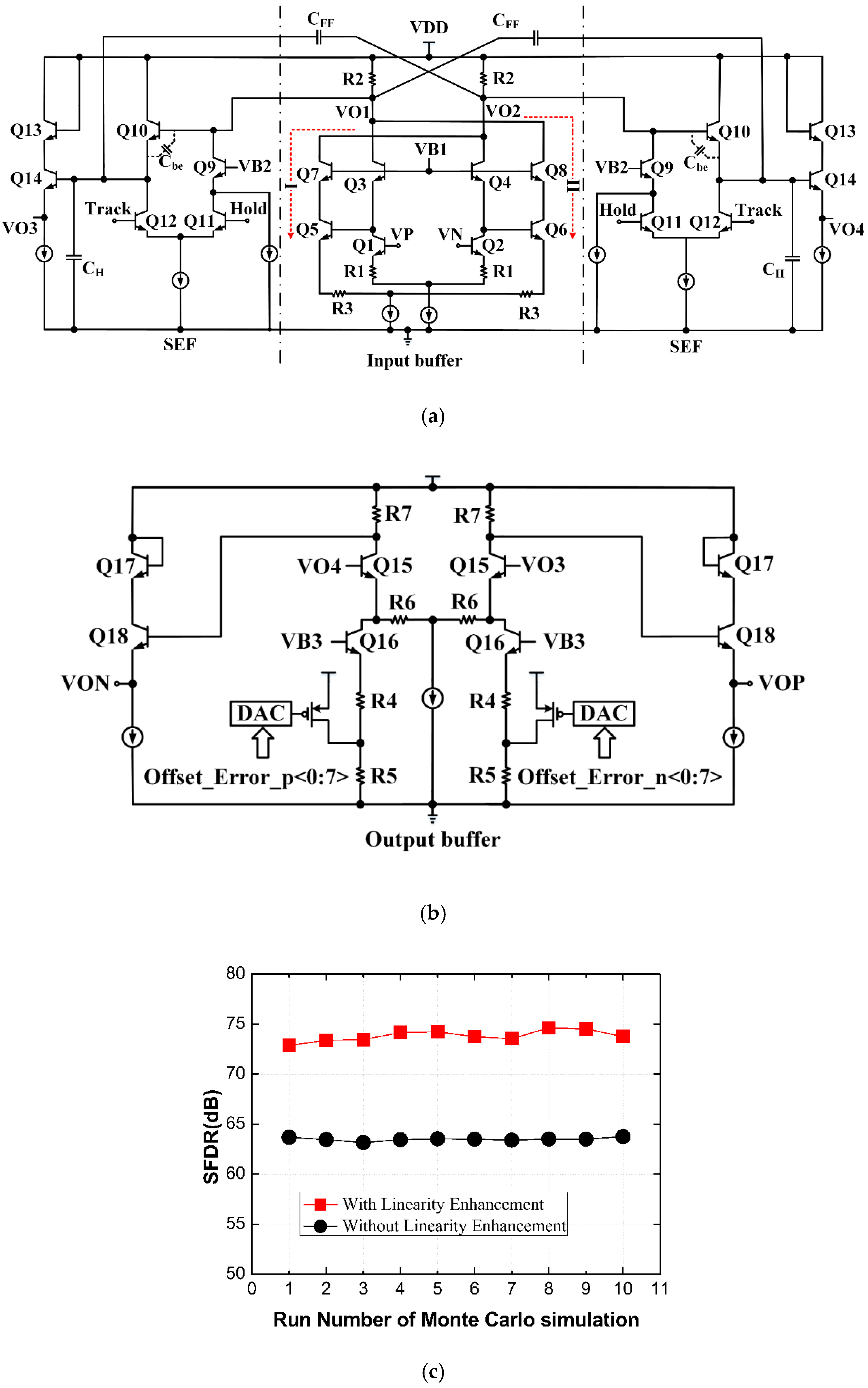
3.1. Track-and-Hold Amplifier

The track-and-hold amplifier (THA) plays an important role in ultra-high-speed F&I ADC, which can alleviate the frequency multiplication effect in the folding process and boost the dynamic performance [14]. The open loop THA consists of an input buffer, switched emitter follower (SEF), and output buffer, as shown in Figure 3.
This input buffer basically behaves as a cascode differential amplifier [15,16], where the emitter degeneration resistor R1 provides local negative feedback to improve linearity. However, the base-emitter voltage Vbe modulation effect of the input transistors still affects the linearity, so branches I (composed of Q5 and Q7) and II (composed of Q6 and Q8) are added for further linearity compensation. If there are no branches I and II,
V I N = V P V N = 2 i × R 1 + V b e 1 V b e 1 = 2 i × R 1 + Δ V b e V O U T = V O 2 V O 1 = 2 i × R 2 = R 2 R 1 × ( V I N Δ V b e )
In the above formula, Vbe1 and Vbe2 are the base-emitter voltages of Q1 and Q2, and their difference is ∆Vbe. The symbol i represents the current variation caused by the change of the input voltage. Evidently, the linearity of VOUT will be degraded by ∆Vbe. After adding branches I and II, Q5 and Q6 convert ∆Vbe into relevant current variations, which are superimposed on the output nodes VO1 and VO2 of the input buffer. Taking branch I as an example for analysis:
Δ V b e Q 1   f o r   v o l t a g e   a m p l i f i c a t i o n A V × Δ V b e Q 5   f o r   c u r r e n t   c o n v e r s i o n A V × Δ V b e × g m
Herein, AV represents the voltage amplification factor of Q1, and gm is the transconductance of Q5, indicating the voltage–current conversion capability.
Branch I converts the ∆Vbe into current variation, which is equal to -α*∆Vbe, where α = AV*gm. Branch II acts similarly except that its current variation is opposite to that of branch I, that is, α × ∆Vbe. Recalculate the output voltage of the input buffer:
V O U T = ( 2 i + 2 α × Δ V b e ) × R 2 = ( V I N Δ V b e R 1 + 2 α × Δ V b e ) × R 2 = R 2 R 1 × V I N + ( 2 α 1 R 1 ) × R 2 × Δ V b e
It can be seen that if 2α = 1/R1 by appropriate design, the influence of ∆Vbe on the output linearity can be eliminated. The comparison of the linearity enhancement effect is shown in Figure 3c, and the Monte Carlo simulation results show that the SFDR is improved by about 10 dB with linearity enhancement. Moreover, as a design consideration of the input buffer, some gain is needed to amplify the narrow input swing. In this topology, the output gain is theoretically determined by R2/R1. Compared to the linearity compensation technique with the diode-type load placed in series on the signal path [17], this structure adds two parallel branches to counteract the modulation effect of Vbe without impairing the signal margin, relaxing the requirements for the power supply voltage.
The SEF is located behind the input buffer and acts as a current switch that controls the current conduction path through the clock signals “Track” and “Hold” to realize signal sampling. The feedforward capacitor CFF is employed to cancel the feed-through effect caused by the parasitic base-emitter junction capacitance Cbe in the holding phase [18].
The output buffer, as shown in Figure 3b, isolates the sampling capacitor CH from the subsequent circuits, and also ensures sufficient driving ability and bandwidth. In addition, the calibration ports, named “Offset_Error_p” and “Offset_Error_n” are reserved for adjusting the output of THA to reduce the offset error. The specific calibration method will be described in detail later.

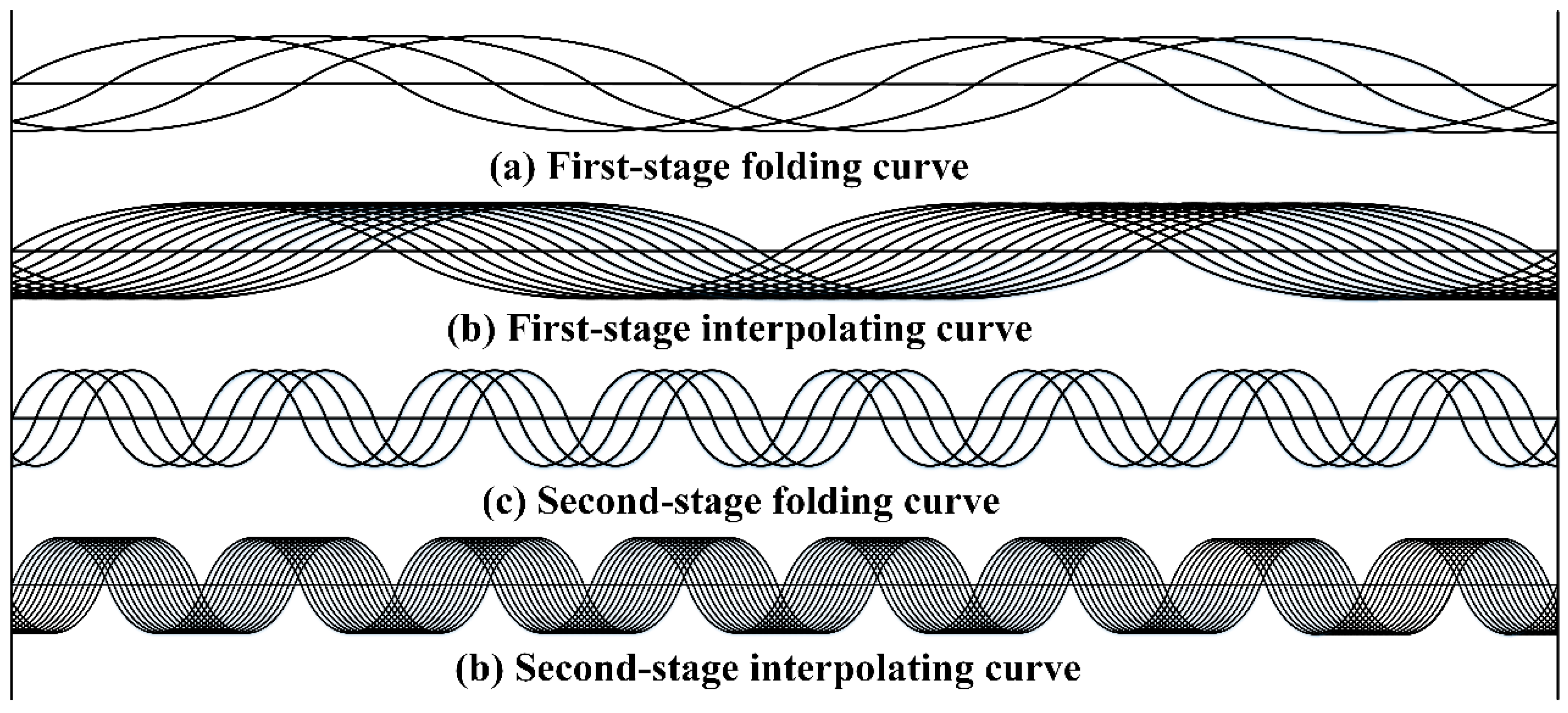
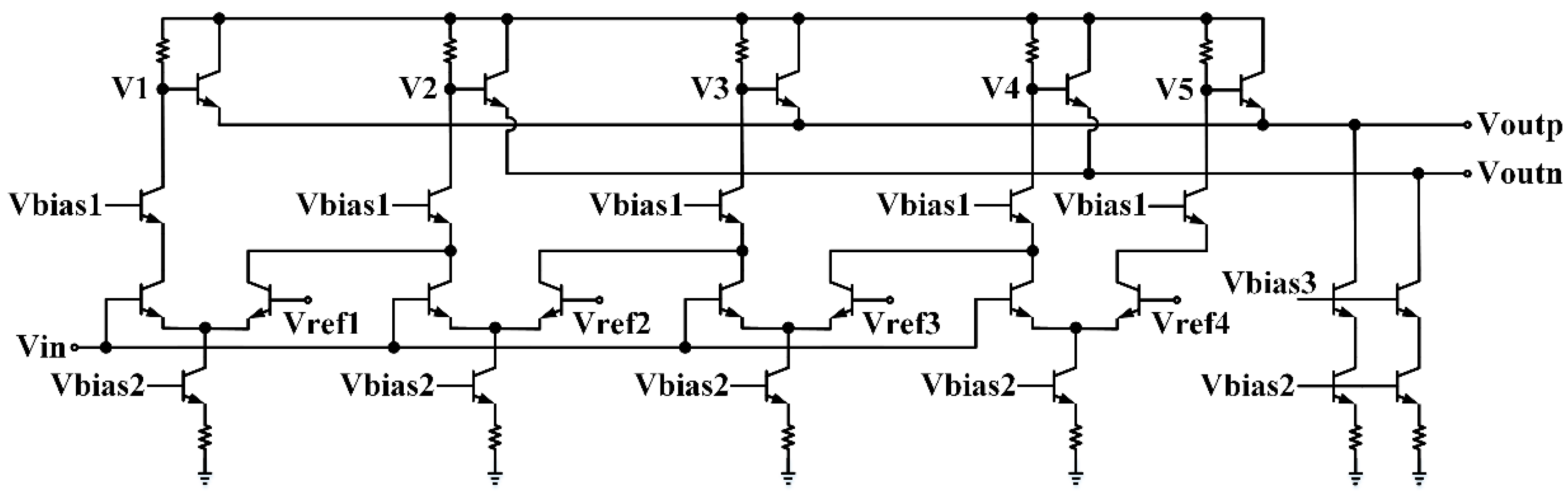
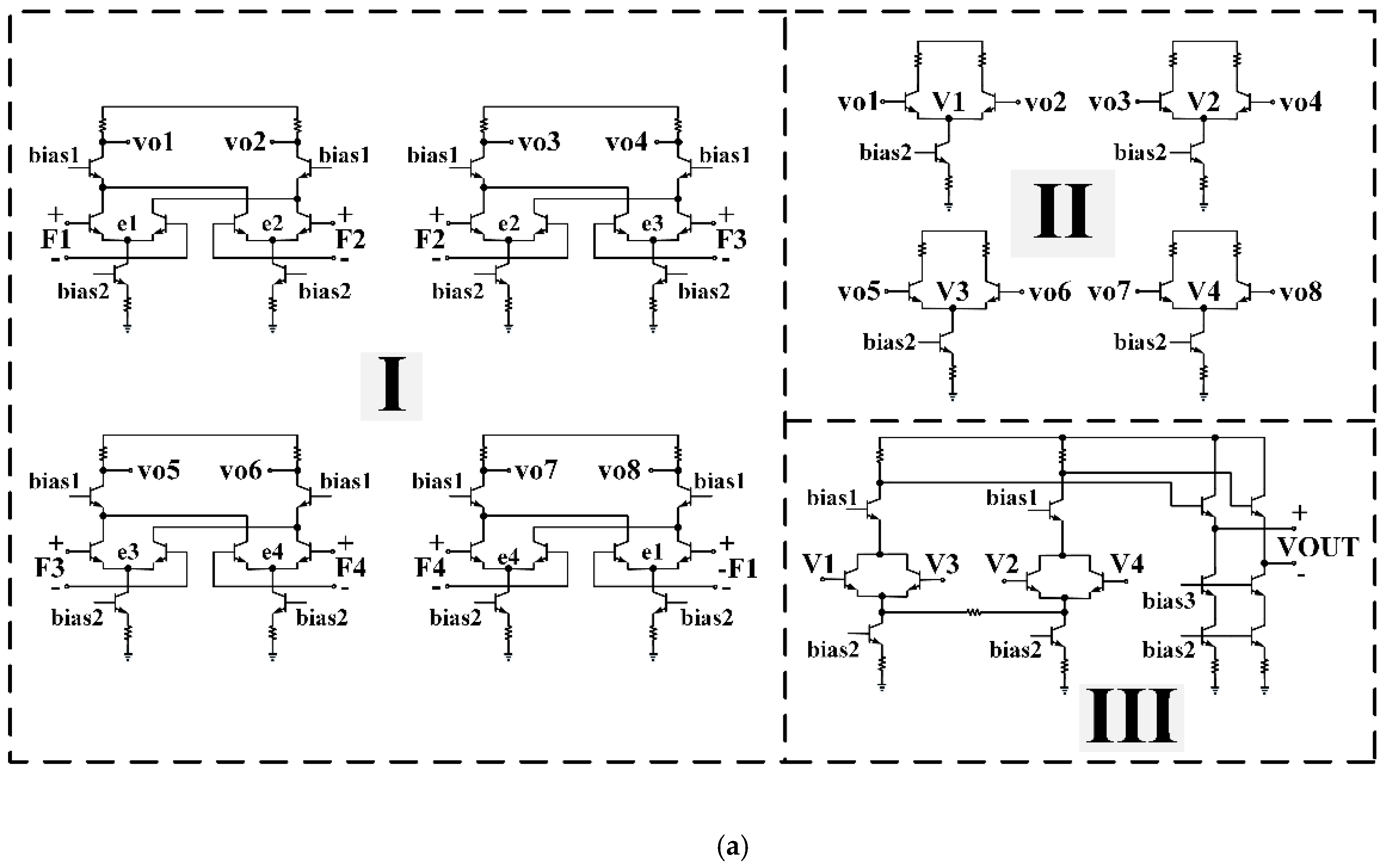
3.2. Folding and Interpolating Circuits

Following the THA, the folding circuits serve to amplify the small voltage difference between the input signal and reference voltages [19] and map the quantization intervals to a segmented folding curve with the reference voltages as zero-crossing points. The first stage folding amplifier incorporates four differential pairs with adjacent collectors connected, as shown in Figure 4.
The internal voltages V1, V3, and V5 are combined by emitter followers, which perform analog “wire-OR” function [20,21], and operation is the same for another set of signals V2 and V4. Finally, a differential folding signal with zero-crossings Vref1~Vref4 is obtained. Besides, V1~V5 are preserved as intermediate signals for further processing to get MSBs. Compared to the conventional “wire-AND” topology where all the outputs of differential pairs are alternatively joined together, this kind of folding amplifier has a much wider bandwidth because the collector parasitic capacitors are not accumulated at the output node [22]. The actual first folding stage comprises four such modules, yielding four primary folding curves of FF = 4, as shown in Figure 2a.
The second stage folding amplifier is used to further increase the folding factor, and its circuit is shown in Figure 5a.
F1~F4 are folding curves from the first stage, and -F1 is the reverse version of F1. The core of part I is a subtraction circuit for amplifying the difference between adjacent differential signals. Then, the differences are detected by part II with the function of “OR,” and all values are combined into a differential output by “NOR” operation in part III. In fact, it is the zero-crossings that carry the quantization information in folding curves, so the focus is on the transformation of zero-crossings proceeding along the signal processing chain. As shown in Figure 5b, a zero-crossing marked as “O” in F1 is taken as a case study. At this point, both F1 and -F1 are zero and F2 = F4. F1-F2 and F4-(-F1) have the same amplitude and opposite phase, so vo1 = vo8 and vo2 = vo7 in part I, making V1 = V4 in part II. Similarly, V2 = V3. Finally, VOUT = 0 in part III, meaning that a zero-crossing of F1 has been transformed into a zero-crossing of the output signal. Likewise, all the zero-crossings of F1~F4 are mapped to the zero-crossings of VOUT one by one, thus realizing the intention of combining the characteristic information of four folding curves into one folding curve. Compared with the solution based on a Gilbert-type multiplier [23,24], this novel structure has fewer transistors stacked on the signal path and larger voltage headroom, beneficial for improving the output voltage swing and optimizing the bias conditions of the transistors. There are four such folding amplifiers in the second stage, absorbing 16 folding curves of FF = 4 from the first stage, and generating four folding curves of FF = 16, as shown in Figure 2c.
Interpolation is used along with folding to generate extra quantization levels between every two neighboring reference voltages, further reducing the number of the folding amplifiers. A resistive interpolation circuit is chosen due to its simplicity and efficiency [25]. The resulting curves from the first and second stage interpolation are shown in Figure 2b,d, respectively.

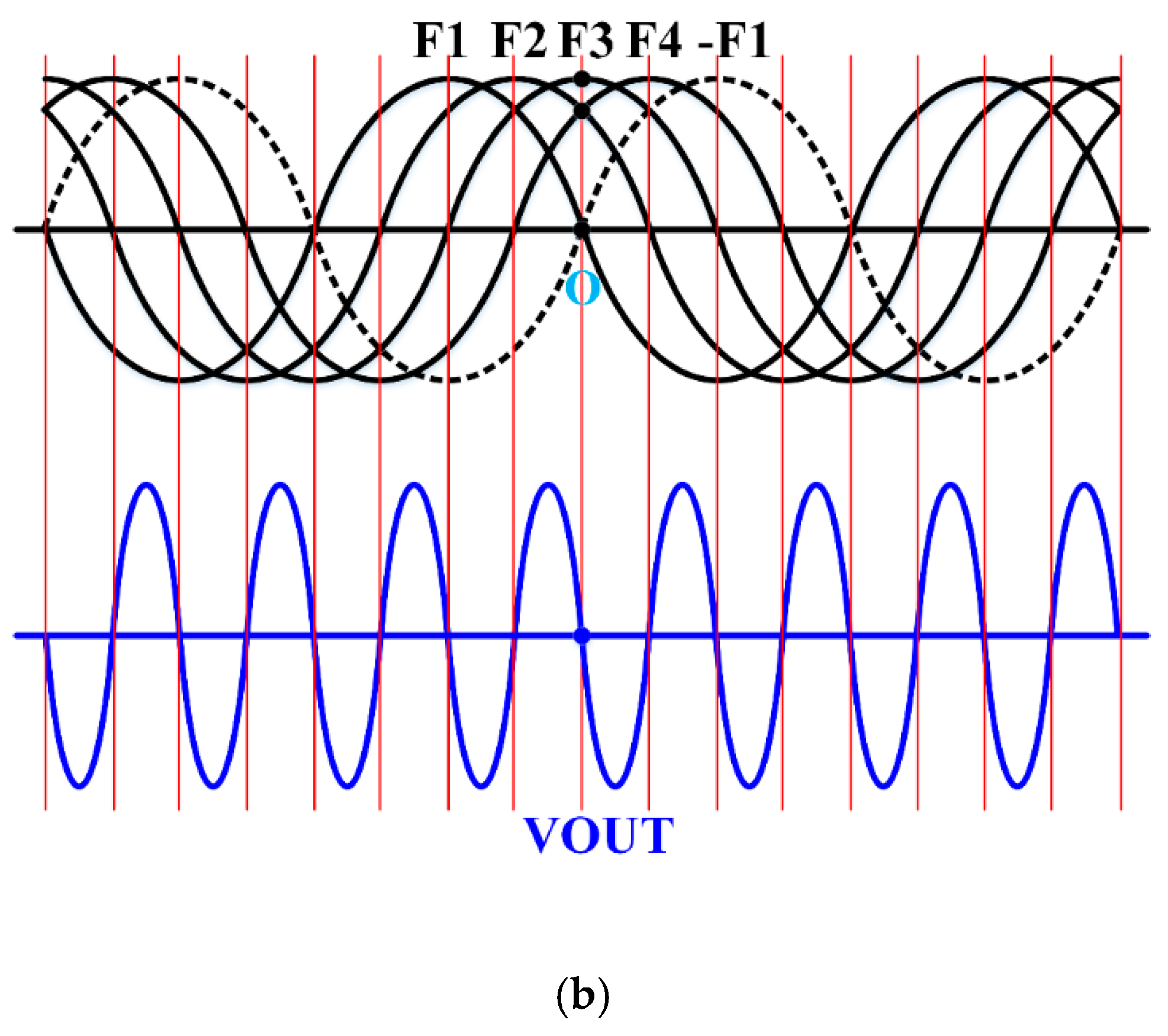
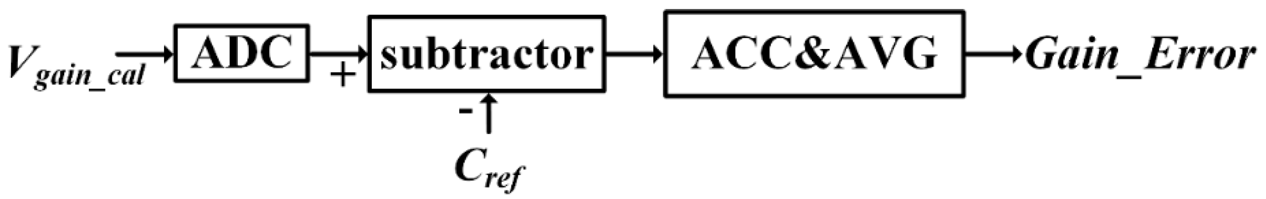
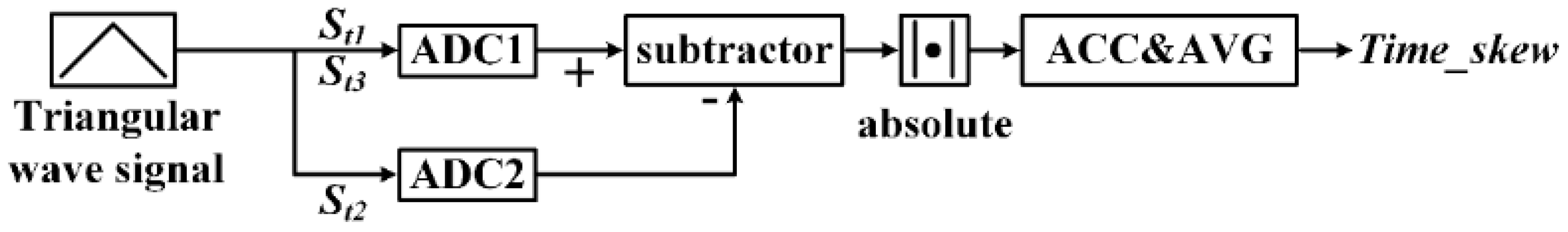
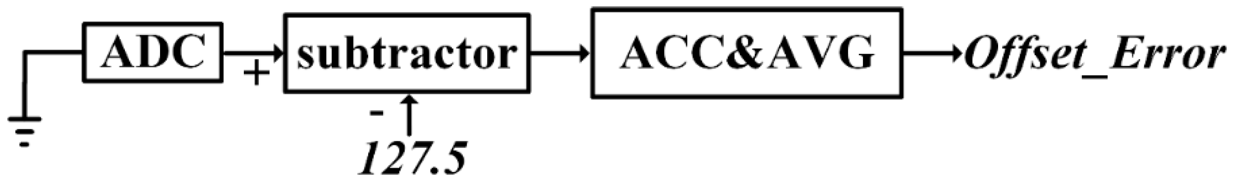
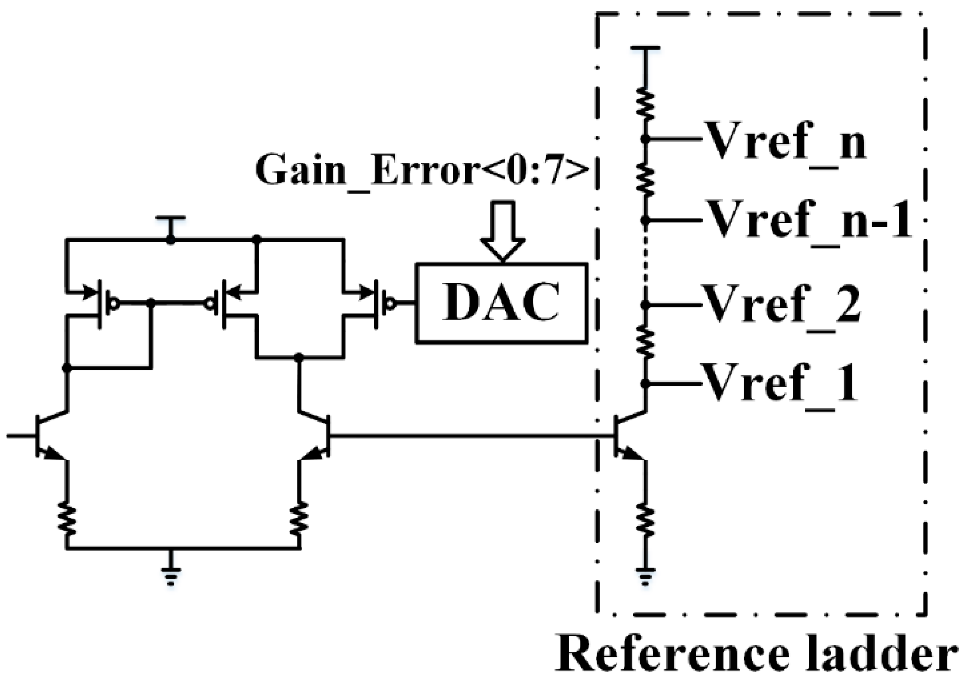
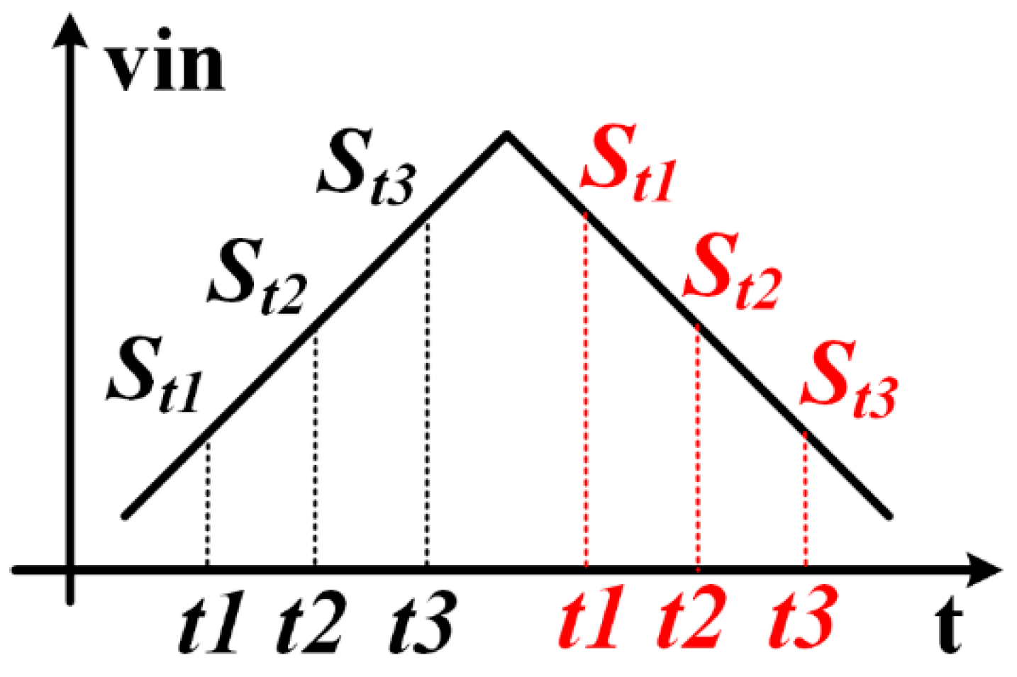
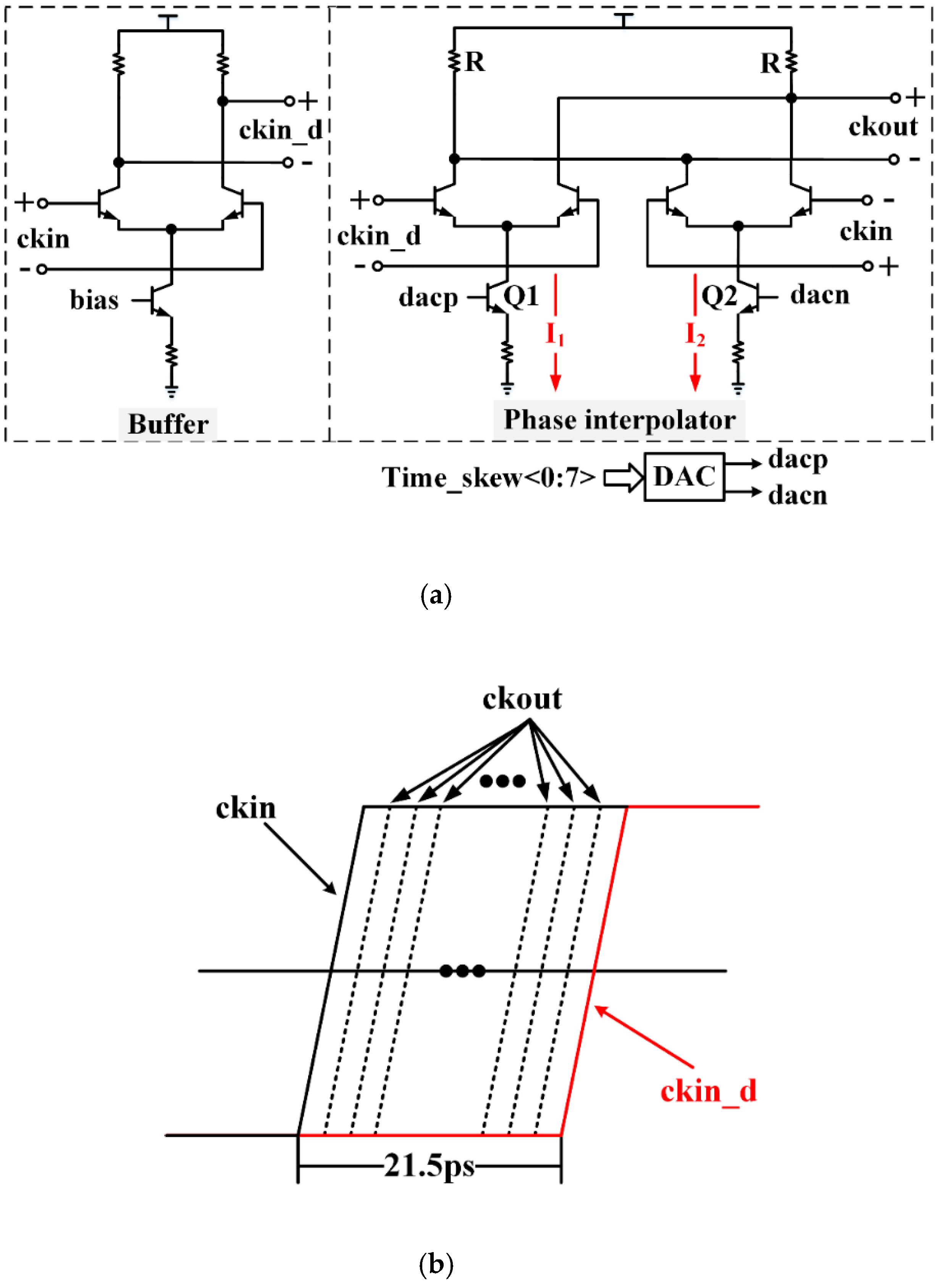
4. Self-Calibration Technique
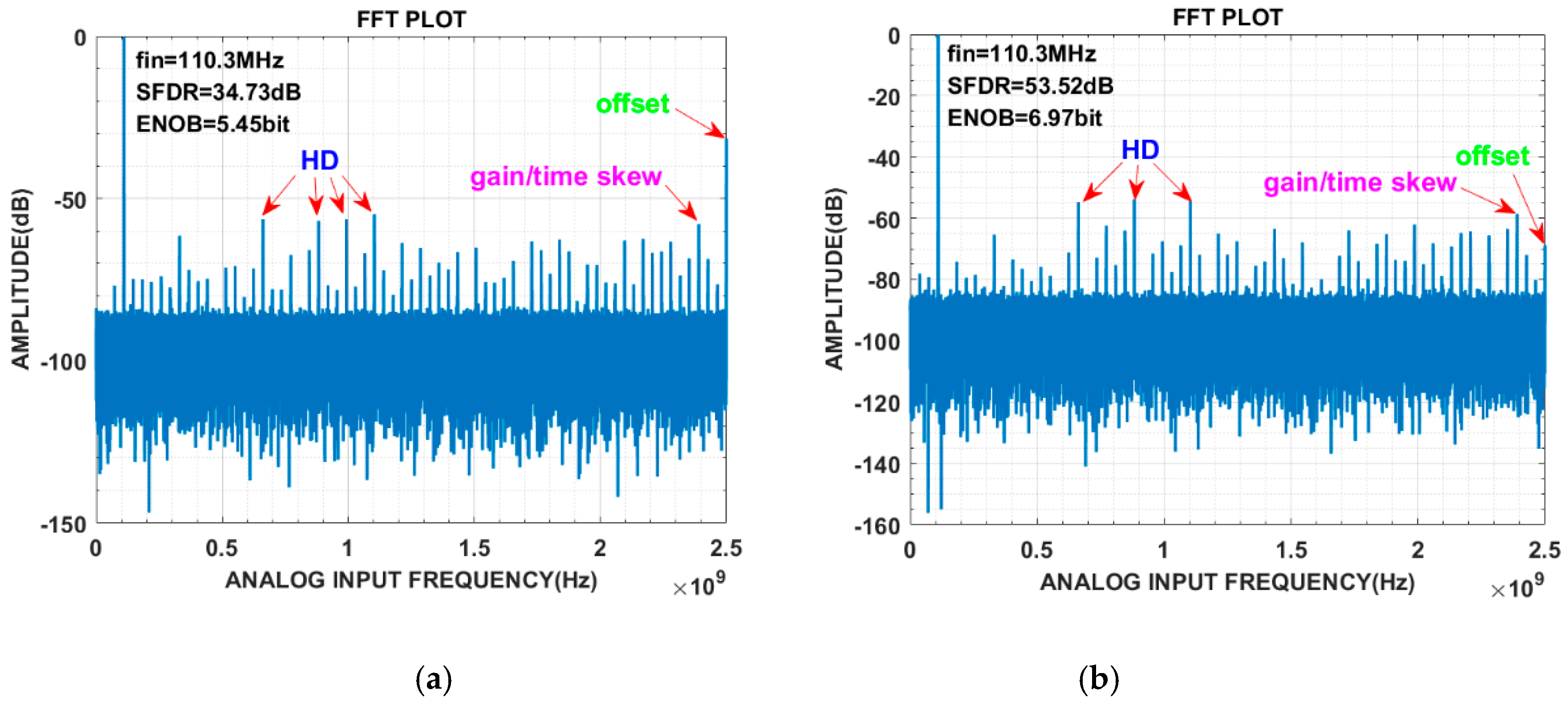
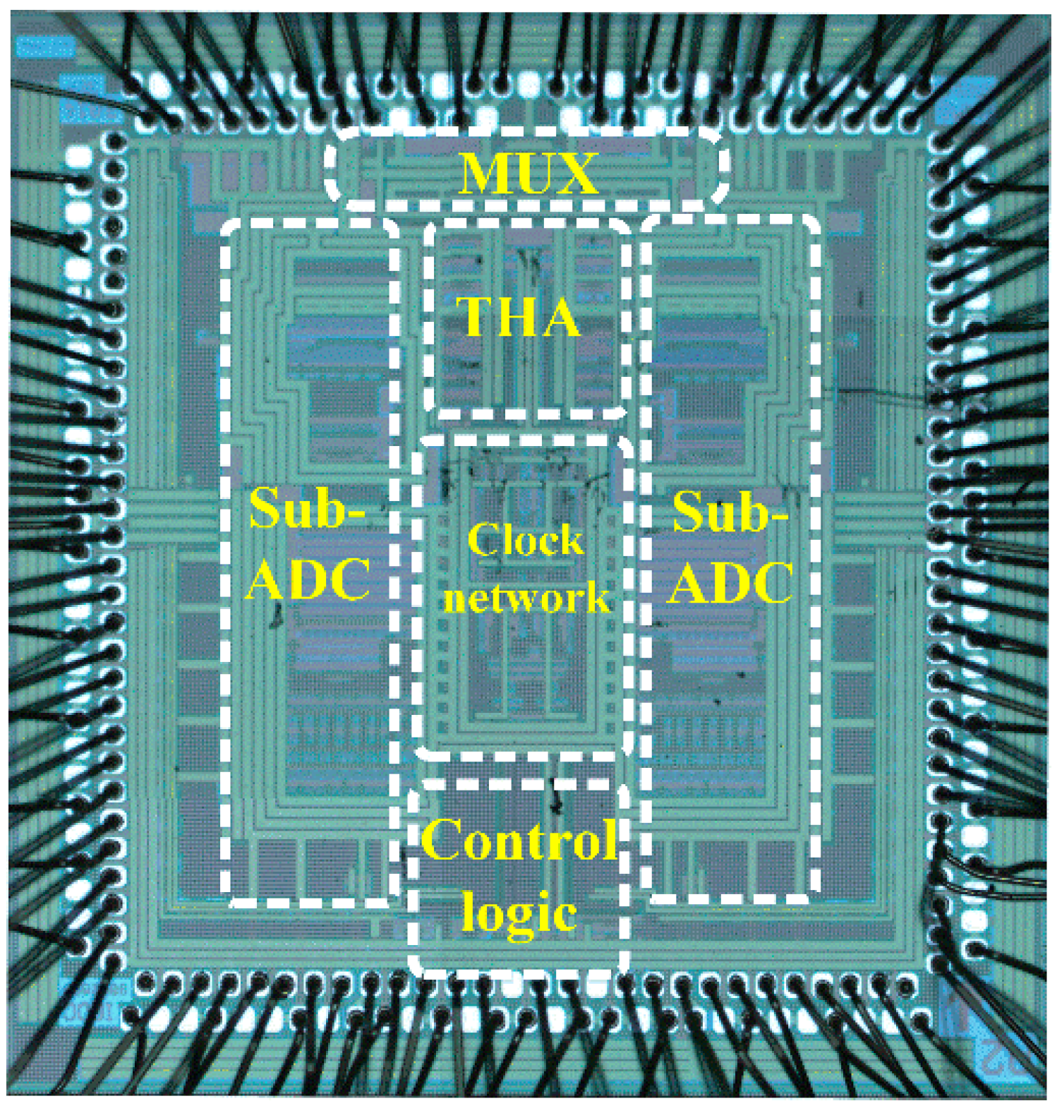
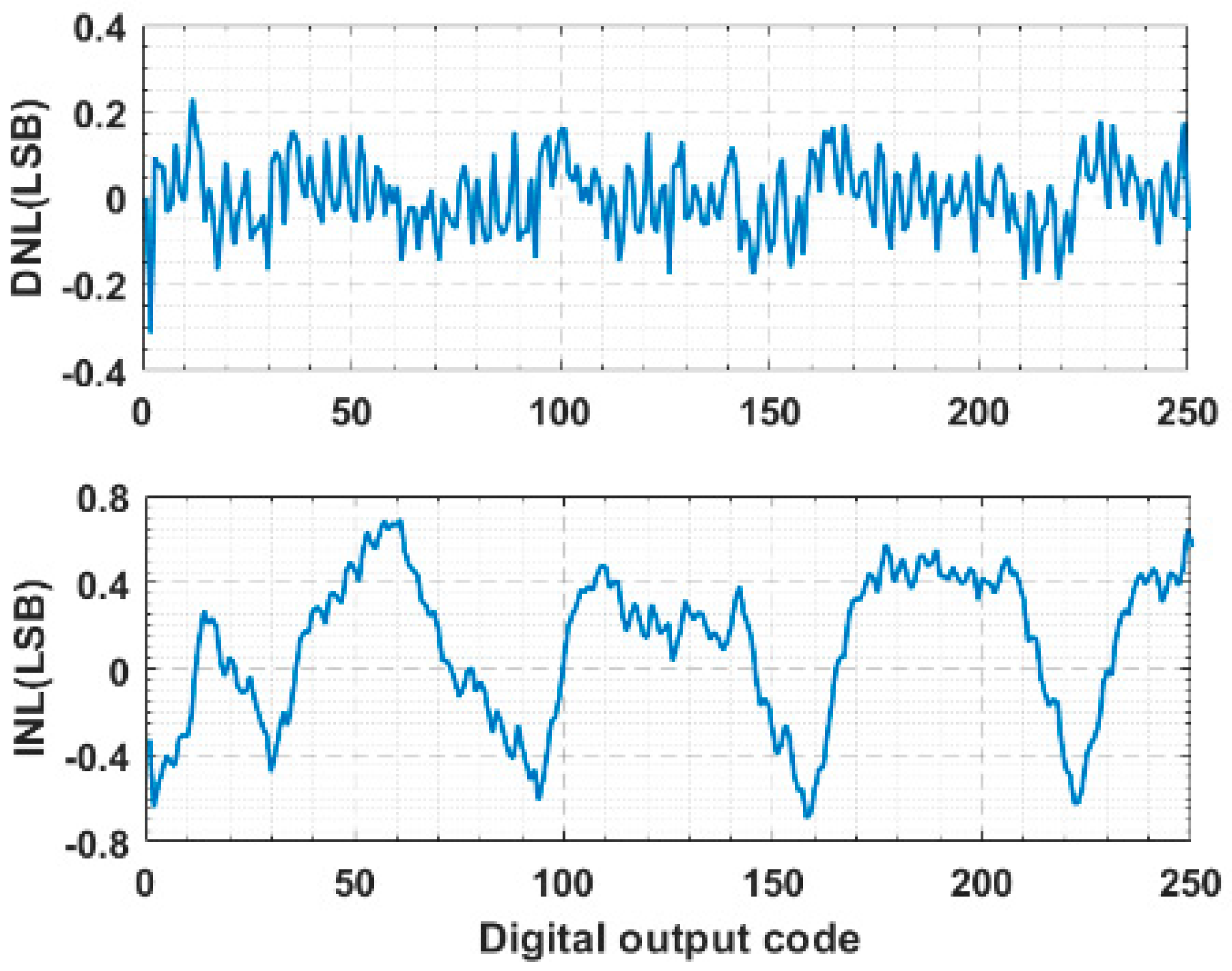
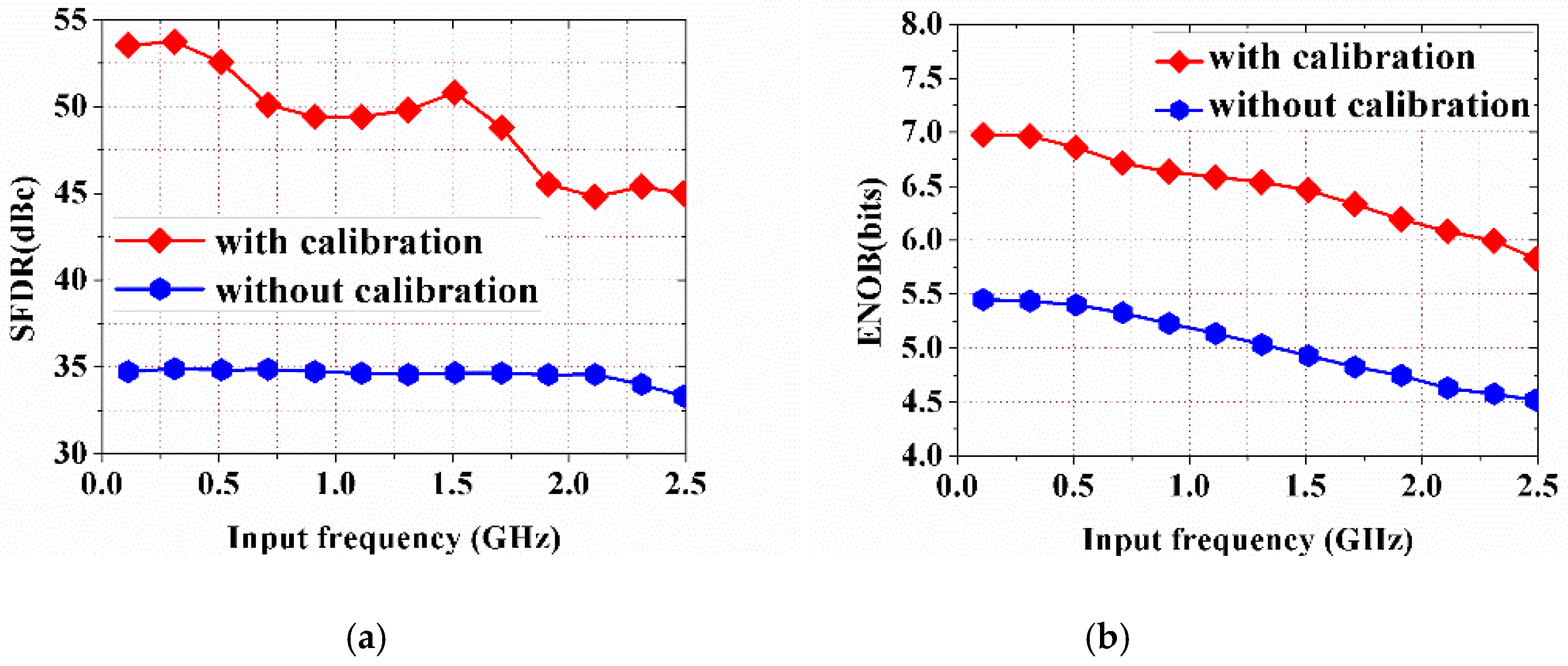
Due to the random mismatch, process variation and design deviation, time-interleaved ADC suffers from offset, gain, and time skew errors between sub-channels. Therefore, calibration is necessary to compensate for these interleaving errors. The on-chip self-calibration method is used with the calibration logic built in the chip, and the whole calibration procedure is automatic without the need for externally applied calibration vectors, making the chip application more convenient.
During the calibration process, the ADC outputs are processed in the digital domain, and the error information is extracted based on statistical estimation, then converted to analog signal by digital-to-analog converter (DAC) and fed back to the internal blocks of the ADC to adjust their operation states in the analog domain. This process forms a negative feedback loop to compensate for the errors iteratively, which is repeated until the error value converges to an acceptable range.
Since the offset and gain mismatches are static errors, their corrections are straightforward and simple, and they can be estimated by giving DC reference voltage to the input of the ADC during the calibration period [26]. In contrast, the time skew mismatch is relatively difficult to correct because the skew-induced error is dependent on signal content [6,27].
For the offset calibration, zero voltage is applied to all sub-ADCs [28]. Theoretically, the zero-level input of ADC corresponds to the median of the output digital codes (that is 127.5 for 8-bit ADC). The actual output digital codes of ADC are subtracted by 127.5, and then the difference is accumulated and averaged (ACC&AVG) to obtain the offset error, as indicated in Figure 6. The calculations involved in this error extraction only consist of simple subtraction operations in combination with averaging, enabling a small and efficient on-chip digital calibration engine instead of a complex software approach [29].
The extracted offset error is converted into an analog signal by an 8-bit current-steering DAC to adjust the bias setting of the THA output buffer, as shown in Figure 3b.
The gain error calibration follows as the offset calibration is completed. A reference voltage Vgain_cal with a fixed DC value is applied to all sub-ADCs [28]. In the ideal case without gain error, a deterministic output digital code labeled Cref is generated and stored as a default reference code. In fact, due to the influence of gain error, ADC may produce a different digital code, which is subtracted by Cref. Then, the difference is accumulated and averaged to obtain the gain error, as shown in Figure 7.
The calibration object for gain error is the resistive reference ladder with an adjustable current source at the bottom [30]. The gain error is fed back and converted into an analog signal by an 8-bit current-steering DAC to regulate the current source and trim the reference voltages, as shown in Figure 8.
The time skew results in the non-uniform sampling of the input signal, which causes sampling errors [31]. The correlation between the quantization results and the sampling time of ADC can be used to estimate the time skew. In the time skew calibration process, a triangular wave serves as the calibration input signal, whose values change linearly with time in the monotonically ascending or descending region. Therefore, the sampling time mismatch can be extracted indirectly based on the statistical information of the quantization results at different sampling instants.
In this design, two sub-ADCs alternately sample the monotonic linear region of the triangular signal in sequence. Assume that the sampling values of sub-ADC1 are St1 and St3, respectively, corresponding to the sampling instants t1 and t3, while for sub-ADC2, the case is St2 and t2. There are two possibilities for the relationship between sampled values, that is, St1 < St2 < St3 in a monotonically rising region or St1 > St2 > St3 in a monotonically decreasing region, as shown in Figure 9. The sampling time mismatch among channels can be reflected by the difference of |St3 - St2| and |St2 - St1|. For example, compared with the ideal sampling of |St2 - St1| = |St3 - St2|, the sampling time of sub-ADC2 is delayed if |St2 - St1| > |St3 - St2| or advanced if |St2 - St1| < |St3 - St2|.
In the actual calibration process, the output digital codes of the ADC, which are one-to-one mapped with the sampled values, are used as the basis for the time skew information extraction. For example, if sub-ADC2 is taken as the reference channel, the output digital codes of sub-ADC1 minus that of sub-ADC2 and the absolute values of the differences are accumulated and averaged to obtain the time skew between the two channels, as shown in Figure 10.
After the time skew is detected, it is converted into analog signals by an 8-bit current-steering DAC, which controls the variable delay cells in the clock network to iteratively adjust the phases of the sampling clocks. The variable delay cell is shown in Figure 11. The sampling clock ckin passes through a buffer to get ckin_d with a relative delay of 21.5 ps, and these two clock signals are input to an analog phase interpolator, which is designed by a pair of differential amplifiers with shared load resistors, acting as a current adder circuit [32]. The delay adjustment is realized by interpolating phase between ckin and ckin_d according to the different weights of the tail currents I1 and I2, which are controlled by an 8-bit current-steering DAC, resulting in a delay adjustment accuracy of 21.5 ps/28 = 84 fs/step.

5. Measured results

The ADC prototype was manufactured in 0.18 μm SiGe BiCMOS technology with a chip size of 3.9 × 3.6 mm2 (including pads). The micrograph is shown in Figure 12.
The static performance of DNL and INL is shown in Figure 13. The measured DNL and INL were −0.31/+0.23 LSB and −0.68/+0.68 LSB, respectively.
The calibration effectiveness is illustrated in Figure 14, where the output fast Fourier transform (FFT) spectrums before and after calibration at 110.3 MHz input frequency are shown. Before calibration, the ADC performance was limited mainly by the mismatches rather than harmonic distortion (HD). After calibration, the SFDR improved from 34.73 dB to 53.52 dB, and the ENOB from 5.45 bit to 6.97 bit.
Figure 15 shows SFDR and ENOB versus input frequency at 5 GS/s. Without calibration, the ADC performance was not satisfactory. In contrast, the calibrated results reveal that the SFDR improved by more than 10 dB and stayed above 44.8 dB up to 2.5 GHz, and the ENOB improved by at least 1.3 bit and greater than 5.8 bit up to 2.5 GHz.
The ADC consumed a total power of 2.8 W and achieved a FoM of 10 pJ/conversion step across the entire first Nyquist zone.
Table 1 gives a performance comparison of ADCs with similar specifications.

6. Conclusions

In this paper, a two-channel time-interleaved 5 GS/s 8-bit F&I ADC fabricated in 0.18 µm SiGe BiCMOS technology has been presented. The on-chip self-calibration technique used to reduce the interleaving errors exhibits lower calibration complexity and a good compensation effect. The ADC shows DNL of -0.31/+0.23 LSB and INL of -0.68/+0.68 LSB. The SFDR stays above 44.8 dB with a peak of 53.52 dB, and the ENOB is greater than 5.8 bit with a maximum of 6.97 bit up to Nyquist frequency. The chip consumes 2.8 W, occupies an area of 3.9 × 3.6 mm2, and realizes a FoM of 10 pJ/conversion step.

Author Contributions

D.W. (Dong Wang) designed the circuits, analyzed the measurement data, and wrote the manuscript. J.L., X.G., and L.Z. assisted with the circuit implementation and simulation. D.W. (Danyu Wu) helped to realize the self-calibration module. H.L. and H.D. performed the chip test. J.W. contributed to the technical discussions and reviewed the manuscript. X.L. gave some valuable guidance and confirmed the final version of the manuscript.

Funding

This research was supported by the National Science and Technology Major Project of China, grant number 2016ZX03001002.

Conflicts of Interest

The authors declare no conflict of interest.

References

  1. Lee, J.; Weiner, J.; Chen, Y.-K. A 20-GS/s 5-b SiGe ADC for 40-Gb/s Coherent Optical Links. IEEE Trans. Circuits Syst. I 2010, 57, 2665–2674. [Google Scholar] [CrossRef]
  2. Ritter, P.; Le Tual, S.; Allard, B.; Möller, M. Design Considerations for a 6 Bit 20 GS/s SiGe BiCMOS Flash ADC Without Track-and-Hold. IEEE J. Solid-State Circuits 2014, 49, 1886–1894. [Google Scholar] [CrossRef]
  3. Du, X.-Q.; Grozing, M.; Buck, M.; Berroth, M. A 40GS/s 4 bit SiGe BiCMOS flash ADC. In Proceedings of the 2017 IEEE Bipolar/BiCMOS Circuits and Technology Meeting (BCTM), Miami, FL, USA, 19–21 October 2017. [Google Scholar]
  4. Fang, J.; Thirunakkarasu, S.; Yu, X.; Silva-Rivas, F.; Zhang, C.; Singor, F.; Abraham, J. A 5-GS/s 10-b 76-mW Time-Interleaved SAR ADC in 28 nm CMOS. IEEE Trans. Circuits Syst. I 2017, 64, 1–11. [Google Scholar] [CrossRef]
  5. Kull, L.; Toifl, T.; Schmatz, M.; Francese, P.A.; Menolfi, C.; Braendli, M.; Kossel, M.; Morf, T.; Andersen, T.M.; Leblebici, Y. A 3.1 mW 8b 1.2 GS/s Single-Channel Asynchronous SAR ADC With Alternate Comparators for Enhanced Speed in 32 nm Digital SOI CMOS. IEEE J. Solid-State Circuits 2013, 48, 3049–3058. [Google Scholar] [CrossRef]
  6. Lin, C.-Y.; Wei, Y.-H.; Lee, T.-C. A 10-bit 2.6-GS/s Time-Interleaved SAR ADC With a Digital-Mixing Timing-Skew Calibration Technique. IEEE J. Solid-State Circuits 2018, 53, 1508–1517. [Google Scholar] [CrossRef]
  7. Buck, M.; Grozing, M.; Bieg, R.; Digel, J.; Du, X.-Q.; Thomas, P.; Berroth, M.; Epp, M.; Rauscher, J.; Schlumpp, M. A 6-GS/s 9.5-b Single-Core Pipelined Folding-Interpolating ADC With 7.3 ENOB and 52.7-dBc SFDR in the Second Nyquist Band in 0.25-µm SiGe-BiCMOS. IEEE Trans. Microwave Theory Techn. 2017, 65, 414–422. [Google Scholar] [CrossRef]
  8. Kuo, W.-M.L.; Lu, Y.; Floyd, B.; Haugerud, B.; Sutton, A.; Krithivasan, R.; Cressler, J.; Gaucher, B.; Marshall, P.; Reed, R.; et al. Proton radiation response of monolithic Millimeter-wave transceiver building blocks implemented in 200 GHz SiGe technology. IEEE Trans. Nucl. Sci. 2004, 51, 3781–3787. [Google Scholar]
  9. Fleetwood, Z.E.; Kenyon, E.W.; Lourenco, N.E.; Jain, S.; Zhang, E.X.; England, T.D.; Cressler, J.D.; Schrimpf, R.D.; Fleetwood, D.M. Advanced SiGe BiCMOS Technology for Multi-Mrad Electronic Systems. IEEE Trans. Device Mater. Relib. 2014, 14, 844–848. [Google Scholar] [CrossRef]
  10. Petrosyants, K.O.; Kozhukhov, M.V. Physical TCAD Model for Proton Radiation Effects in SiGe HBTs. IEEE Trans. Nucl. Sci. 2016, 63, 2016–2021. [Google Scholar] [CrossRef]
  11. Leroy, M.R.; Raman, S.; Chu, M.; Kim, J.-W.; Guo, J.-R.; Zhou, K.; You, C.; Clarke, R.; Goda, B.; McDonald, J.F.; et al. High-Speed Reconfigurable Circuits for Multirate Systems in SiGe HBT Technology. Proc. IEEE 2015, 103, 1181–1196. [Google Scholar] [CrossRef]
  12. Lal, D.; Ali, A.M.A.; Ricketts, D.S. Analysis and Comparison of High-Resolution GS/s Samplers in Advanced BiCMOS and CMOS. IEEE Trans. Circuits and Sys. II Express Briefs 2018, 65, 532–536. [Google Scholar] [CrossRef]
  13. Jiang, F.; Wu, D.; Zhou, L.; Wu, J.; Jin, Z.; Liu, X. An 8-bit 1 GS/s folding and interpolating ADC with a base-4 architecture. Analog Integr. Circuits Signal Process. 2013, 76, 139–146. [Google Scholar] [CrossRef]
  14. Li, Y.; Sanchez-Sinencio, E. A wide input bandwidth 7-bit 300-msample/s folding and current-mode interpolating adc. IEEE J. Solid-State Circuits 2003, 38, 1405–1410. [Google Scholar]
  15. Halder, S.; Gustat, H.; Scheytt, C. An 8 Bit 10 GS/s 2Vpp Track and Hold Amplifier in SiGe BiCMOS Technology. In Proceedings of the 2010 Proceedings of ESSCIRC, Montreux, Switzerland, 19–21 September 2006. [Google Scholar]
  16. Avitabile, G.; Cascella, D.; Cannone, F.; Coviello, G. Low distortion input buffer for high resolution GS/s rate track-and-hold amplifiers. Electron. Lett. 2012, 48, 755. [Google Scholar] [CrossRef]
  17. Fung, Q.; Fomani, A.A.; Feng, Y.; Ng, W.T. Design of a 2-GSample/s Track-and-Hold Amplifier implemented in a 60-GHz SiGe BiCMOS Process. In Proceedings of the 2007 IEEE Conference on Electron Devices and Solid-State Circuits, Tainan, Taiwan, 20–22 December 2007. [Google Scholar]
  18. Wu, D.; Jiang, F.; Zhou, L.; Wu, J.; Huang, Y.; Jin, Z.; Liu, X. A 4GS/s 8bit ADC fabricated in 0.35µm SiGe BiCMOS technology. In Proceedings of the 2013 IEEE Bipolar/BiCMOS Circuits and Technology Meeting (BCTM), Bordeaux, France, 30 September–3 Octomber 2013. [Google Scholar]
  19. Taft, R.; Menkus, C.; Tursi, M.; Hidri, O.; Pons, V. A 1.8-V 1.6-GSample/s 8-b self-calibrating folding ADC with 7.26 ENOB at Nyquist frequency. IEEE J. Solid-State Circuits 2004, 39, 2107–2115. [Google Scholar] [CrossRef]
  20. Van de Grift, R.; Rutten, I.W.J.M.; van der Veen, M. An 8-bit video ADC incorporating folding and interpolation techniques. IEEE J. Solid-State Circuits 1987, 22, 944–953. [Google Scholar] [CrossRef]
  21. Vessal, F.; Salama, C. An 8-bit 2-Gsample/s folding-interpolating analog-to-digital converter in SiGe technology. IEEE J. Solid-State Circuits 2004, 39, 238–241. [Google Scholar] [CrossRef]
  22. Jiang, F.; Wu, D.; Zhou, L.; Huang, Y.; Wu, J.; Jin, Z.; Liu, X. A wideband calibration-free 1.5-GS/s 8-bit analog-to-digital converter with low latency. Analog Integr Circ Sig Process 2014, 81, 341–348. [Google Scholar] [CrossRef]
  23. Vorenkamp, P.; Roovers, R. A 12-b, 60-MSample/s cascaded folding and interpolating ADC. IEEE J. Solid-State Circuits 1997, 32, 1876–1886. [Google Scholar] [CrossRef]
  24. Razzaghi, A.; Tam, S.-W.; Kalkhoran, P.; Wang, Y.; Kuan, C.-Y.; Nissim, B.; Vu, L.D.; Chang, M.-C.F. A single-channel 10b 1GS/s ADC with 1-cycle latency using pipelined cascaded folding. In Proceedings of the 2008 IEEE Bipolar/BiCMOS Circuits and Technology Meeting, Monteray, CA, USA, 13–15 October 2008. [Google Scholar]
  25. Nakajima, Y.; Sakaguchi, A.; Ohkido, T.; Kato, N.; Matsumoto, T.; Yotsuyanagi, M. A Background Self-Calibrated 6b 2.7 GS/s ADC With Cascade-Calibrated Folding-Interpolating Architecture. IEEE J. Solid-State Circuits 2010, 45, 707–718. [Google Scholar] [CrossRef]
  26. Miki, T.; Ozeki, T.; Naka, J.-I. A 2-GS/s 8-bit Time-Interleaved SAR ADC for Millimeter-Wave Pulsed Radar Baseband SoC. IEEE J. Solid-State Circuits 2017, 52, 2712–2720. [Google Scholar] [CrossRef]
  27. Kundu, S.; Alpman, E.; Lu, J.H.-L.; Lakdawala, H.; Paramesh, J.; Jung, B.; Zur, S.; Gordon, E. A 1.2 V 2.64 GS/s 8 bit 39 mW Skew-Tolerant Time-interleaved SAR ADC in 40 nm Digital LP CMOS for 60 GHz WLAN. IEEE Trans. Circuits Syst. I 2015, 62, 1929–1939. [Google Scholar] [CrossRef]
  28. Hsu, C.-C.; Huang, F.-C.; Shih, C.-Y.; Huang, C.-C.; Lin, Y.-H.; Lee, C.-C.; Razavi, B. An 11b 800MS/s Time-Interleaved ADC with Digital Background Calibration. In Proceedings of the 2007 IEEE International Solid-State Circuits Conference. Digest of Technical Papers, San Francisco, CA, USA, 11–15 February 2007. [Google Scholar]
  29. Doris, K.; Janssen, E.; Nani, C.; Zanikopoulos, A.; Van Der Weide, G. A 480 mW 2.6 GS/s 10b Time-Interleaved ADC With 48.5 dB SNDR up to Nyquist in 65 nm CMOS. IEEE J. Solid-State Circuits 2011, 46, 2821–2833. [Google Scholar] [CrossRef]
  30. Kertis, R.A.; Humble, J.S.; Daun-Lindberg, M.A.; Philpott, R.A.; Fritz, K.E.; Schwab, D.J.; Prairie, J.F.; Gilbert, B.K.; Daniel, E.S. A 20 GS/s 5-Bit SiGe BiCMOS Dual-Nyquist Flash ADC With Sampling Capability up to 35 GS/s Featuring Offset Corrected Exclusive-Or Comparators. IEEE J. Solid-State Circuits 2009, 44, 2295–2311. [Google Scholar] [CrossRef]
  31. El-Chammas, M.; Murmann, B. A 12-GS/s 81-mW 5-bit Time-Interleaved Flash ADC With Background Timing Skew Calibration. IEEE J. Solid-State Circuits 2011, 46, 838–847. [Google Scholar] [CrossRef]
  32. Agazzi, O.E.; Hueda, M.R.; Crivelli, D.E.; Carrer, H.S.; Nazemi, A.; Luna, G.; Ramos, F.; Lopez, R.; Grace, C.; Kobeissy, B.; et al. A 90 nm CMOS DSP MLSD Transceiver With Integrated AFE for Electronic Dispersion Compensation of Multimode Optical Fibers at 10 Gb/s. IEEE J. Solid-State Circuits 2008, 43, 2939–2957. [Google Scholar] [CrossRef]
  33. Chan, B.; Oyama, B.; Monier, C.; Gutierrez-Aitken, A. An Ultra-Wideband 7-Bit 5-Gsps ADC Implemented in Submicron InP HBT Technology. IEEE J. Solid-State Circuits 2008, 43, 2187–2193. [Google Scholar] [CrossRef]
Figure 1. The block diagram of the analog-to-digital converter (ADC).
Electronics 08 00253 g001
Figure 2. Radix-4 two-stage cascaded folding and interpolating curves.
Electronics 08 00253 g002
Figure 3. (a) Input buffer and switched emitter follower (SEF) in the track-and-hold amplifier (THA); (b) Output buffer with offset calibration interface; (c) Comparison of linearity enhancement effect.
Electronics 08 00253 g003
Figure 4. The folding amplifier in the first stage.
Electronics 08 00253 g004
Figure 5. (a) The folding amplifier in the second stage; (b) The input and output signals.
Electronics 08 00253 g005aElectronics 08 00253 g005b
Figure 6. Offset error extraction diagram.
Electronics 08 00253 g006
Figure 7. Gain error extraction diagram.
Electronics 08 00253 g007
Figure 8. Reference ladder with gain error calibration interface.
Electronics 08 00253 g008
Figure 9. Triangular wave as the calibration input signal.
Electronics 08 00253 g009
Figure 10. Time skew extraction diagram.
Electronics 08 00253 g010
Figure 11. (a) Variable delay cell for time skew calibration; (b) The diagram of phase interpolating.
Electronics 08 00253 g011
Figure 12. Micrograph of the proposed ADC.
Electronics 08 00253 g012
Figure 13. Measured differential nonlinearity (DNL) and integral nonlinearity (INL).
Electronics 08 00253 g013
Figure 14. Output fast Fourier transform (FFT) spectrum (a) before calibration; (b) after calibration.
Electronics 08 00253 g014
Figure 15. (a) Spurious free dynamic range (SFDR) versus input frequency; (b) Effective number of bits (ENOB) versus input frequency.
Electronics 08 00253 g015
Table 1. Comparison of the analog-to-digital converter (ADC) performance.
Parameter[1][8][11][33]This work
Technology0.25 µm SiGe0.35 µm SiGe47 GHz
SiGe
0.8 µm InP0.18 µm SiGe
ArchitectureF&ITI F&IF&IF&ITI F&I
Sample frequency (GS/s)64255
Resolution (bits)9.58878
ENOB (bits)
@Nyquist frequency
7.35.56.25.75.8
DNL/INL (LSB)1.2/3.50.3/0.80.5/1.0N.A.0.31/0.68
Core power (W)10.23.038.42.8
FoM (pJ/conv.step) 110.816.5123210
Calibrationnoyesnonoyes
1 FoM = Power/(2ENOB × Sampling frequency).

