16.8/15.2 ppm/°C 81 nW High PSRR Dual-Output Voltage Reference for Portable Biomedical Application

Abstract
:1. Introduction
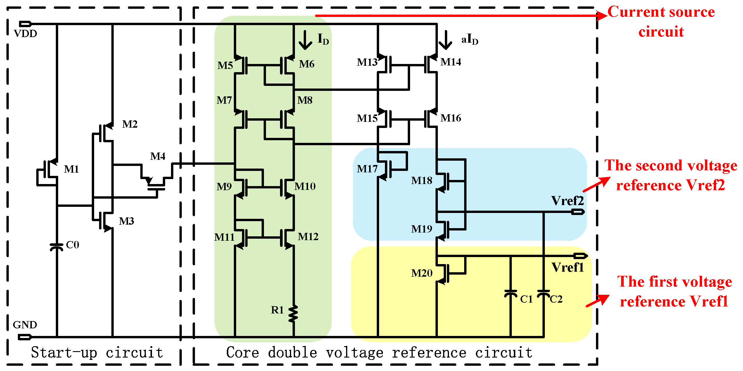
2. Circuit Design
2.1. Start-up Circuit
2.2. Current Source Circuit
2.3. The Vref1 Generator Circuit
2.4. The Vref2 Generator Circuit
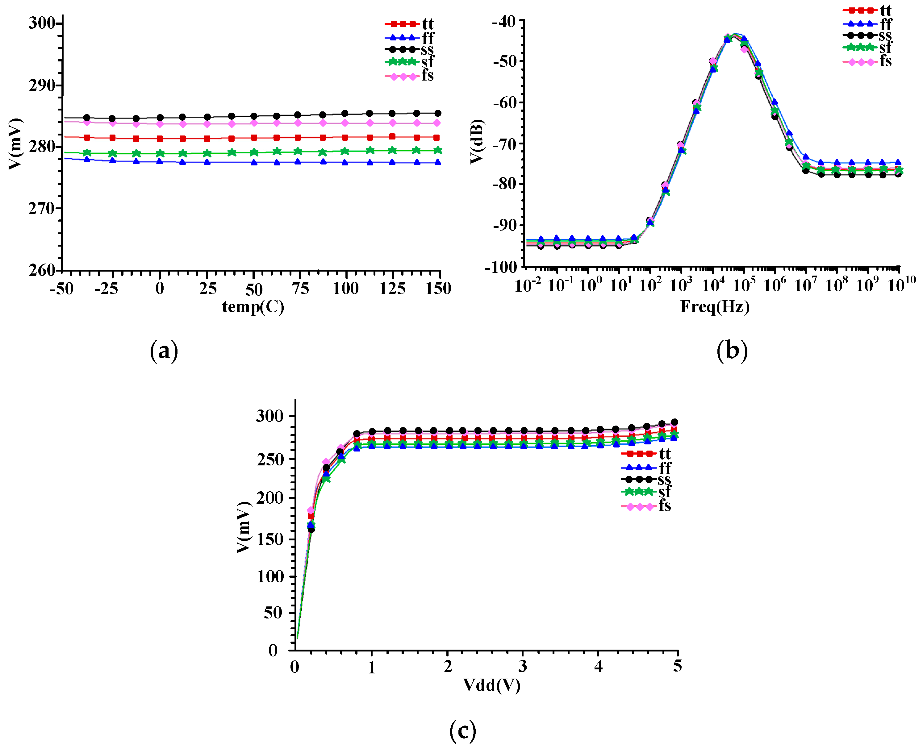
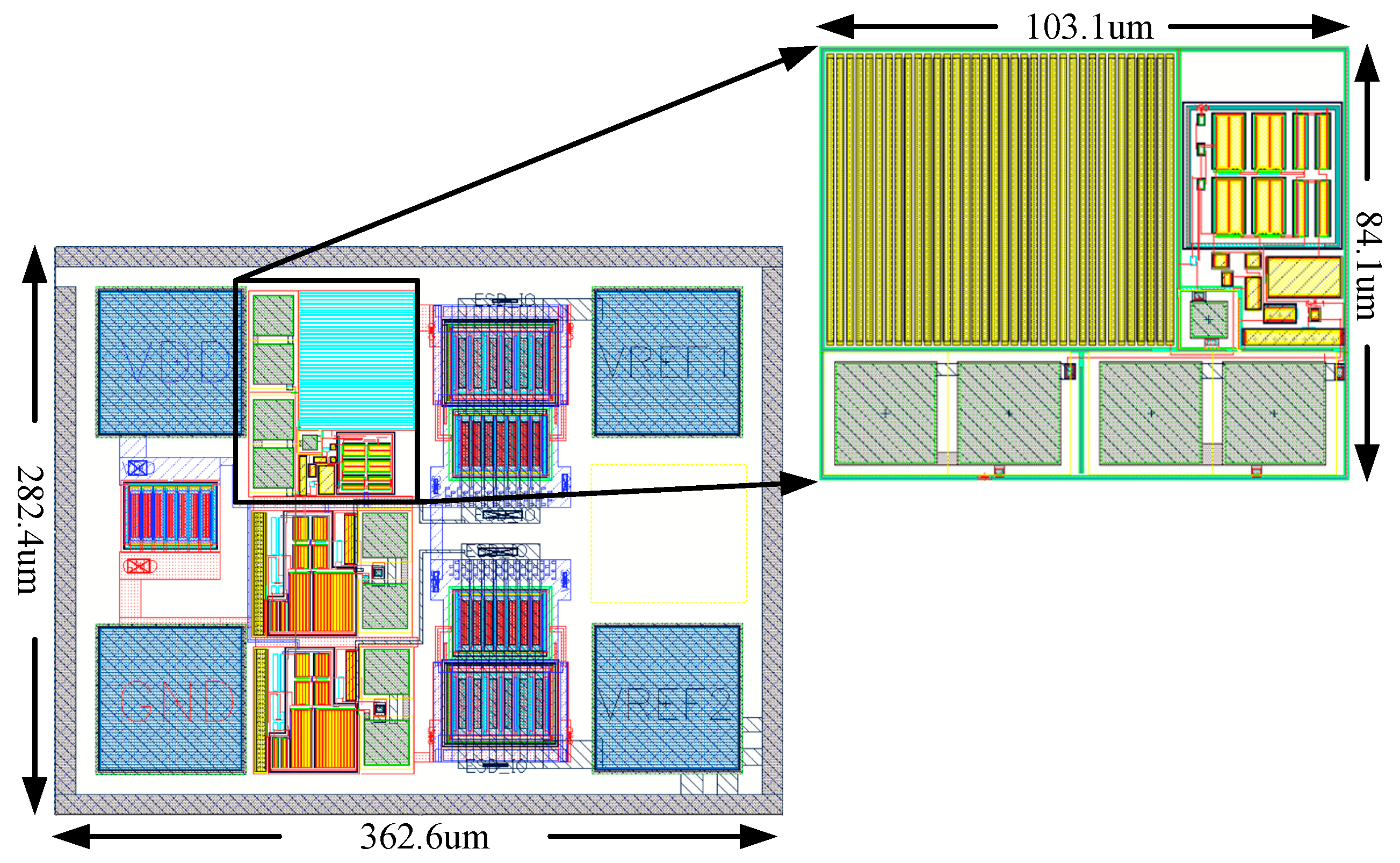
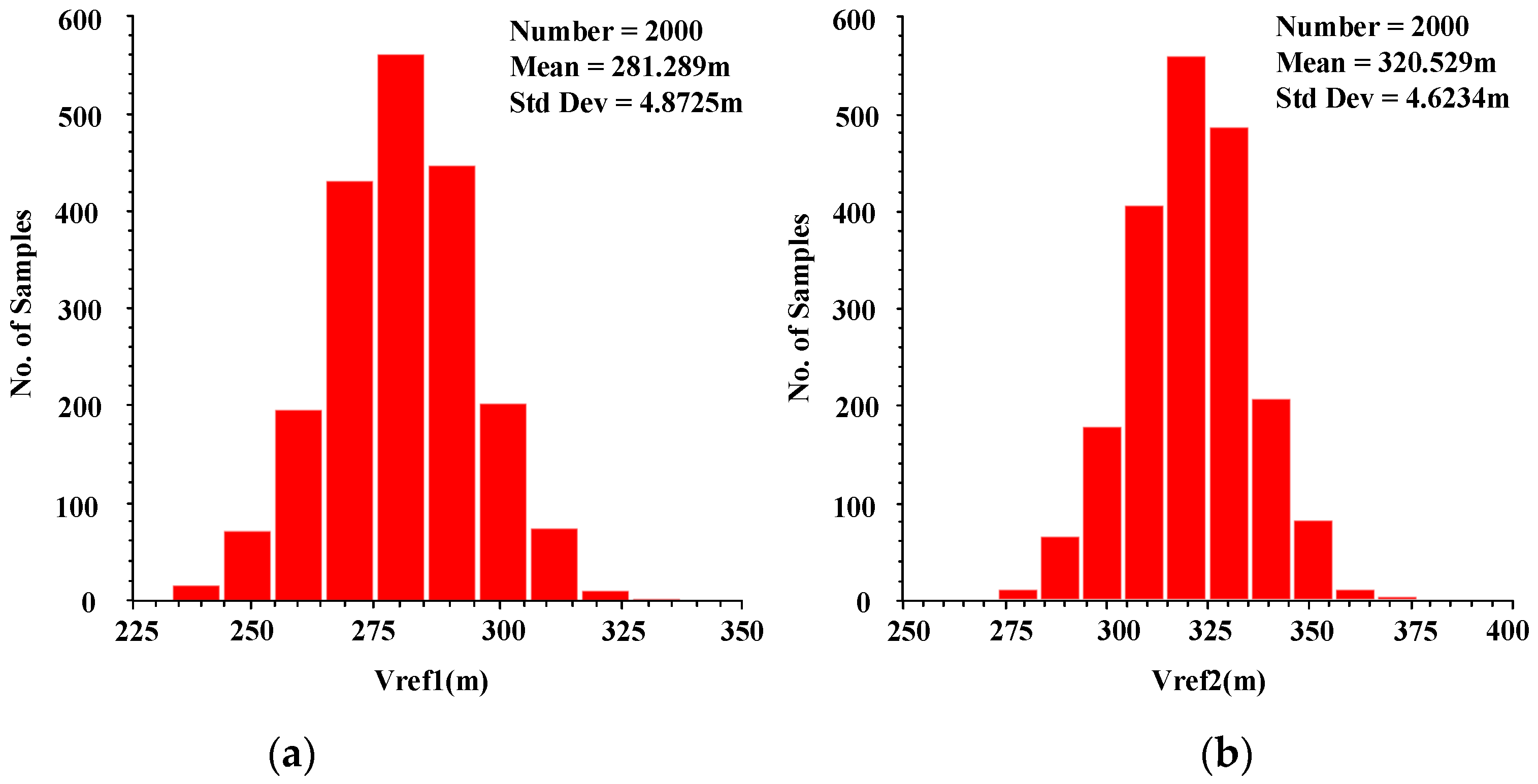
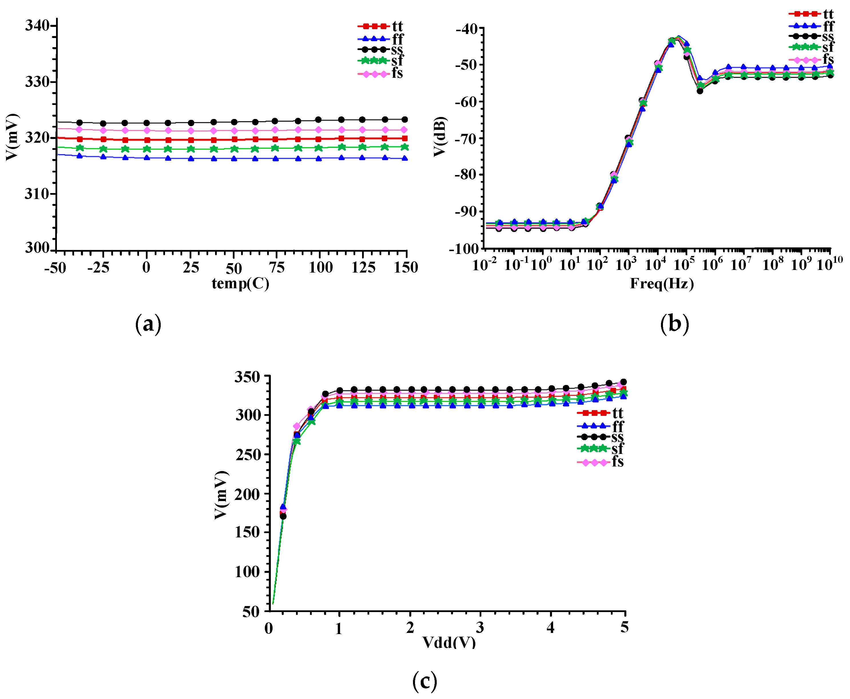
3. Simulation Results
4. Discussion
5. Conclusions
Author Contributions
Funding
Conflicts of Interest
References
- Wang, Y.; Zhu, Z.; Yao, J.; Yang, Y. A 0.45-V, 14.6-nW CMOS Subthreshold Voltage Reference With No Resistors and No BJTs. IEEE Trans. Circuits Syst. Express Briefs 2015, 62, 621–625. [Google Scholar] [CrossRef]
- Chen, H.-M.; Lee, C.-C.; Jheng, S.-H.; Chen, W.-C.; Lee, B.-Y. A Sub-1 ppm/°C Precision Bandgap Reference with Adjusted-Temperature-Curvature Compensation. IEEE Trans. Circuits Syst. Regul. Pap. 2017, 64, 1308–1317. [Google Scholar] [CrossRef]
- Osaki, Y.; Hirose, T.; Kuroki, N.; Numa, M. 1.2-V Supply, 100-nW, 1.09-V Bandgap and 0.7-V Supply, 52.5-nW, 0.55-V Subbandgap Reference Circuits for Nanowatt CMOS LSIs. IEEE J. Solid-State Circuits 2013, 48, 1530–1538. [Google Scholar] [CrossRef]
- Ueno, K.; Hirose, T.; Asai, T.; Amemiya, Y. A 300 nW, 15 ppm/°C, 20 ppm/V CMOS Voltage Reference Circuit Consisting of Subthreshold MOSFETs. IEEE J. Solid-State Circuits 2009, 44, 2047–2054. [Google Scholar] [CrossRef]
- Ashrafi, S.F.; Atarodi, S.M.; Chahardori, M. New low voltage, high PSRR, CMOS bandgap voltage reference. In Proceedings of the IEEE International SoC Conference, Newport Beach, CA, USA, 17–20 September 2008. [Google Scholar]
- Wang, L.; Zhan, C.; Tang, J.; Liu, Y.; Li, G. A 0.9-V 33.7-ppm/°C 85-nW Sub-Bandgap Voltage Reference Consisting of Subthreshold MOSFETs and Single BJT. IEEE Trans. VLSI Syst. 2018, 26, 2190–2194. [Google Scholar] [CrossRef]
- Hao, Z.; Bo, Z.; Zhao-Ji, L.; Ping, L. A New CMOS Current Reference with High Order Temperature Compensation. In Proceedings of the 2006 International Conference on Communications, Circuits and Systems, Guilin, China, 25–28 June 2006; Volume 4, pp. 2189–2192. [Google Scholar]
- Duan, J.; Zhu, Z.; Deng, J.; Xu, W.; Wei, B. A Novel 0.8-V 79-nW CMOS-Only Voltage Reference With −55-dB PSRR @ 100 Hz. IEEE Trans. Circuits Syst. Express Briefs 2018, 65, 849–853. [Google Scholar] [CrossRef]
- Razavi, B. Design of Analog CMOS Integrated Circuits, 1st ed.; Xian Jiaotong University Press: Xian, China, 2003; pp. 23–24. [Google Scholar]
- Luo, Y.; Zhang, J.; Wang, Q.; Zeng, Y.; Hu, J.; Tan, H.-Z. An ultra-low power CMOS subthreshold voltage reference. In Proceedings of the 2012 IEEE International Conference on Electron Devices and Solid State Circuit (EDSSC), Bangkok, Thailand, 3–5 December 2012. [Google Scholar]
- Liu, L.; Mu, J.; Zhu, Z. A 0.55-V, 28-ppm/°C, 83-nW CMOS Sub-BGR With UltraLow Power Curvature Compensation. IEEE Trans. Circuits Syst. I 2018, 65, 95–106. [Google Scholar] [CrossRef]
- Zeng, Y.; Li, Y.; Zhang, X.; Tan, H.-Z. Ultra-low-power, high PSRR CMOS voltage reference with negative feedback. IET Circuits Devices Syst. 2017, 11, 535–542. [Google Scholar] [CrossRef]


| Transistor | W/L (µm/µm) | Transistor | W/L (µm/µm) |
|---|---|---|---|
| M1 | 0.42/0.42 | M12 | 5.9/2 |
| M2 | 0.42/0.42 | M13 | 10/1 |
| M3 | 0.42/0.42 | M14 | 10/1 |
| M4 | 0.42/0.42 | M15 | 10/1 |
| M5 | 2*10/2 | M16 | 10/1 |
| M6 | 2*10/2 | M17 | 5.5/2 |
| M7 | 2*10/2 | M18 | 14/7 |
| M8 | 2*10/2 | M19 | 1.6/1.25 |
| M9 | 2.5/2 | M20 | 2.3/18 |
| M10 | 2.5/2 | Resistance | (kΩ) |
| M11 | 2.4/1 | R1 | 635.4 |
| Corner | TC (−40°C–150°C) (ppm/°C) | PSRR (dB) | LS (0.9 V–3.1 V) (%/V) | Min Power (nW) | |
|---|---|---|---|---|---|
| @100 Hz | @1 MHz | ||||
| Vref2tt | 16.8 | −88.9 | −52.8 | 0.11 | 81.4 |
| Vref1tt | 15.2 | −89.9 | −76.7 | 0.11 | |
| Vref2ff | 31.2 | −89.4 | −51.4 | 0.10 | 94.05 |
| Vref1ff | 28.5 | −90.2 | −75.1 | 0.10 | |
| Vref2ss | 36.5 | −88.6 | −54.1 | 0.08 | 73.3 |
| Vref1ss | 42.7 | −89.6 | −78.1 | 0.08 | |
| Vref2fs | 18.1 | −89.0 | −52.5 | 0.08 | 77.5 |
| Vref1fs | 12.9 | −89.8 | −77.0 | 0.08 | |
| Vref2sf | 26.1 | −88.8 | −53.2 | 0.09 | 85.45 |
| Vref1sf | 29.1 | −89.8 | −76.4 | 0.09 | |
| Parameter | [1] | [2] | [3] | [11] | [12] | This Work | |
|---|---|---|---|---|---|---|---|
| CMOS technology (nm) | 180 | 180 | 180 | 130 | 180 | 180 | |
| Supply voltage (V) | 0.45–1.8 | 1.3–1.8 | 1.1–1.8/0.7–1.8 | 1.2 | 0.85–2.5 | 0.9–3.1 | |
| VREF (mV) | 118.46 | 547 | 1090/548 | 735 | 634.1 | 320.5/281 | |
| Temperature Range (/°C) | −40–125 | −40–140 | −40–120 | −40–120 | −20–80 | −40–150 | |
| Average TC (ppm/°C) | 63.6 | 1.67 | 147/114 | 9.3 | 16.3 | 16.8/15.2 | |
| Line Sensitivity (%/V) | 1.2 | 0.08 | 0.737/1.05 | - | 0.086 | 0.11/0.11 | |
| PSRR (dB) | @100 Hz | −44.2 | −55 | −62/−56 | −30 | −83 | −88.9/−89.9 |
| @1 MHz | −26.3 | - | - | - | >−64 | −52.8/−76.7 | |
| Min Power (nW) | 14.4@4.5 V | - | 100@1.1/52.5@0.7 V | 30.5@0.6 V | 202@0.85 V | 81.4@0.9 V | |
| Area (mm2) | 0.012 | 0.0094 | 0.054 | 0.063 | 0.01 | 0.0086 | |
© 2019 by the authors. Licensee MDPI, Basel, Switzerland. This article is an open access article distributed under the terms and conditions of the Creative Commons Attribution (CC BY) license (http://creativecommons.org/licenses/by/4.0/).
Share and Cite
Yue, H.; Sun, X.; Liu, J.; Xu, W.; Li, H.; Wei, B.; Wang, T.; Lin, S. 16.8/15.2 ppm/°C 81 nW High PSRR Dual-Output Voltage Reference for Portable Biomedical Application. Electronics 2019, 8, 213. https://doi.org/10.3390/electronics8020213
Yue H, Sun X, Liu J, Xu W, Li H, Wei B, Wang T, Lin S. 16.8/15.2 ppm/°C 81 nW High PSRR Dual-Output Voltage Reference for Portable Biomedical Application. Electronics. 2019; 8(2):213. https://doi.org/10.3390/electronics8020213
Chicago/Turabian StyleYue, Hongwei, Xiaofei Sun, Junxin Liu, Weilin Xu, Haiou Li, Baolin Wei, Taotao Wang, and Siyu Lin. 2019. "16.8/15.2 ppm/°C 81 nW High PSRR Dual-Output Voltage Reference for Portable Biomedical Application" Electronics 8, no. 2: 213. https://doi.org/10.3390/electronics8020213
APA StyleYue, H., Sun, X., Liu, J., Xu, W., Li, H., Wei, B., Wang, T., & Lin, S. (2019). 16.8/15.2 ppm/°C 81 nW High PSRR Dual-Output Voltage Reference for Portable Biomedical Application. Electronics, 8(2), 213. https://doi.org/10.3390/electronics8020213