Abstract
In this research work, we investigated a dual switch (DS) active rectifier for the piezoelectric (PE) energy scavenging system. In the proposed DS active rectifier configuration, two extra switches are shunted across the PE transducer which helps the PE transducer’s capacitor in charging and discharging which results in maximum power extraction from the PE transducer. Moreover, in the proposed rectifier configuration comparator controlled active diodes are used instead of conventional/passive diodes to minimize the threshold voltage drop. The proposed DS active rectifier design is fabricated in a 1-poly 6-metal 180-nm standard CMOS process. The simulation and measured results of the proposed DS active rectifier design have the better power conversion efficiency (PCE) of 91.5 %, which definitely helps in extracting more power than the conventional full bridge rectifier (FBR).
1. Introduction
Energy Scavenging or Harvesting is a process in which energy can be derived/extracted from the various environmental sources like solar, thermal, RF, etc. [1,2,3,4]. Piezoelectric elements (PE) can be used to produce electrical energy from mechanical energy and it is quite a promising solution because of higher power density versus internal light and electromagnetic/electrostatic vibration. Usually, the PE transducers output is an irregular function of time and it needs to be rectified first to be usable. The most commonly used AC–DC converters are the conventional full bridge rectifiers (FBR) and half wave rectifiers. The drawback of these rectifiers is low power extraction and low conversion efficiency which introduced a switch only (single switch) rectifier [2,3]. It almost doubles the power extraction efficiency by the addition of a single switch across the PE transducer when it is compared with the conventional FBR circuit. In [2], the forward voltage drops across the rectifying diodes were a major source of conduction power loss and this issue is minimized by the use of the comparator based active diodes [3]. The work in [3,4,5,6] has designed the active rectifier and [3] redesign it and use it with a single switch which improves the power conversion efficiency [7,8,9]. In this research work, we introduce a dual switch active rectifier with high-power extraction and better conversion efficiency implemented on a 180-nm Complementary metal oxide semiconductor transistor (CMOS) process. An efficiency of 91.5% is achieved and this number is better than other reported rectifiers.
2. Proposed Rectifier and Circuit Implementation
2.1. Proposed DS Active Rectifier
The PE transducer shown in Figure 1 is usually modelled as a current source shunted with the capacitor and a resistor i.e., and , where is the amplitude of the current and is the excitation frequency. The PE transducer output is not usable directly, as it is in a sinusoidal shape. It has to be rectified first and then it can be usable by the load circuits [1,2,3,4,5]. In order to increase the conversion efficiency of the conventional FBR as well as other rectifiers proposed in [1,2], we propose a CMOS dual switch (DS) active rectifier shown in Figure 1. In the proposed rectifier, two P-type (PMOS) transistors, MP1 and MP2, are configured in cross-coupled structure while other N-type (NMOS) transistors are implemented by using comparators and combined with two NMOS transistors MN1 and MN2. Two symmetrical switches in parallel with the PE transducer are used to discharge the PE transducer capacitor completely. When the switch voltage Switch voltage (VSW) turns on for a brief time, it discharges the PE transducer capacitor completely through the ground. is the output capacitor and is used to store the harvested energy while is the load resistor.
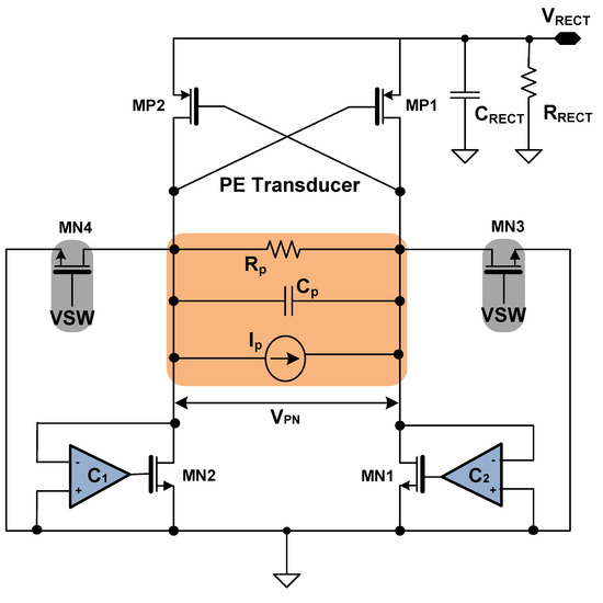
Figure 1.
Schematic of the proposed DS active rectifier [3,10,11].
2.2. Operation Principle of Proposed DS Active Rectifier
Initially, the current of PE transducer shown in Figure 1 is used to charge . As further increases i.e., increases and decreases. When the difference of and i.e., = − is greater than the threshold voltage |Vthp| of the transistor, it turned on MP1. is shorted to output , further increase in decreases , and it switched the comparators output to a high state and this turns on transistor MN2. As a result, a current path to load capacitor is formed as both the transistors MP1 and MN2 are turned on. When approaches zero, the switch VSW turns on shortly and discharges completely the PE transducer capacitor by shortening the nodes and to the ground. At this time, = 0 and both the transistor MP1 and MN2 turn off too, and the first cycle ends. In the next half cycle, the proposed DS active rectifier operates in a similar manner except that, now, MP2 and MN1 are involved. The adoption of two symmetrical switches help to charge and discharge instantly to transfer as much energy as possible.
2.3. Power Conversion and Extraction Analysis
For further understanding of the proposed rectifier, we analyze the power extraction and conversion process of the conventional full bridge rectifier (FBR). The conventional FBR with ideal diodes , its current pulse , and waveform across the PE transducer i.e., is shown in Figure 2.
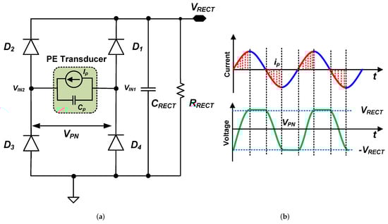
Figure 2.
(a) Schematic diagram of the conventional FBR; (b) Associated current and voltage waveforms.
Figure 2 shows that available charge in the PE transducer is not completely delivered at the output [2]. The shaded portion shows that, at every half cycle, the amount of charge is not delivered at the output, and the current waveform from the PE transducer has to charge the capacitor from to before the diodes turns on. This losted charge limits the amount of power that can be extracted using the conventional FBR. The charge that actually flows into the output capacitor is just the difference between the total available charge and the lost charge [2]. The amount of charge available from the PE transducer is given as [12]
where and , the open circuit voltage is given as . The Equation (1) can be written as
The charge per cycle lost will be
The actual charge that flows into the output capacitor per cycle is the difference between the total charge available and charge lost per cycle is given by
The total energy per cycle is
Now the total power delivered at the output can be calculated using
It is obvious that power vary with and at , it reach at its maximum value, than maximum power is
The actual charge that flows at the
The total energy delivered to every cycle is given by
The power delivered to the output by DS active rectifier is the product of the charge delivered and frequency as
The maximum power can be extracted by using DS active rectifier is
There are two major issues in conventional FBR. The first is its very poor power extraction capability and other one is the voltage drop across the diodes which results power losses. To overcome these issues, we propose DS active rectifier. The DS active rectifier combines the advantages of both conventional FBR and switch only rectifier in [2]. Figure 3 shows the current and voltage waveforms associated with the DS active rectifier. The switches across the PE transducer turned on for a brief time to discharge its capacitor to ground at every zero crossing of the PE transducer current .
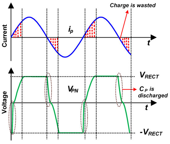
Figure 3.
Current and voltage waveforms associated with the proposed DS active rectifier.
3. Results and Discussion
The proposed DS active rectifier shown in Figure 1 is implemented in 180-nm CMOS technology and is simulated and measured with the following transducer parameters, = 490 A, = 130 nF, = 200 Hz, and = 1 M. The values of load resistor and capacitor are 200 K and 1 F, respectively.
For comparison, a cross-coupled rectifier is implemented too. The transient voltages at the input and output of the proposed DS active rectifier and cross-coupled rectifier is shown in Figure 4. It is obvious that the use of two switches in parallel with the PE transducer, discharges the capacitor to ground twice in a cycle, when current crosses zero which results in higher value and higher power extraction compared to the cross-coupled active rectifier. It also shows the comparison of rectified output voltage and the input voltage of the DS active rectifier and cross-coupled rectifier. The in flipping case is higher than the conventional one.
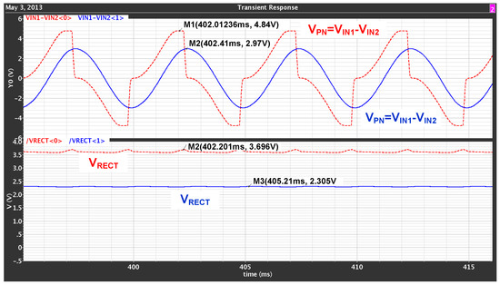
Figure 4.
Comparison of transient voltage at the input and output of the proposed DS active rectifier and conventional cross-coupled rectifier.
Figure 5 shows the rectified output voltage of the DS active rectifier and cross-coupled rectifier is 3.91 and 2.15 V, respectively. It starts from zero, when the PE-transducer is at rest. The output voltage increases when the traducer starts vibrating and reached at its steady state. The proposed DS rectifier is simulated at different corners (tt, ff, ss) as well as for the verification of the design functionality are shown in Figure 6. It is shown that the maximum rectified output voltage can be seen at ’tt’, while comparable rectified out voltage can be seen at ’ff’ and ’ss’. This is because at ‘ss’ the threshold voltages of NMOS/PMOS becomes low which results in a low rectified output voltage. The same will happen at ‘ff’ corner as NMOS/PMOS transistors threshold voltage becomes high [13]. The theoretical maximum output power of the proposed and conventional cross-coupled rectifier is 468 and 234 W, respectively, and the calculated power of proposed and cross-coupled rectifier is 427 and 189 W, respectively. The active area of the proposed DS active rectifier is 53 × 18 m and is shown in Figure 7. The efficiency of the proposed DS active rectifier is 91.5%. The performance summary of the proposed DS active rectifier and its comparison with other reported rectifiers is shown in Table 1. It is shown that the voltage and efficiency is the best when it is compared with the other reported designs in the literature [14,15,16,17,18,19]. The measured results of the proposed DS active rectifier are shown in Figure 8. For the measurement the PE transducer’s equivalent model circuit is used instead of the actual PE transducer. It consists of an AC voltage source in series with a capacitor is used. A sine wave of 200 Hz with 3-V pk-pk is placed in series with the = 130 nF. The measured waveform , the control signal VSW and the rectified output voltage is shown in Figure 8. The measured output voltage is 3.61 V while in simulation it is 3.91 V.
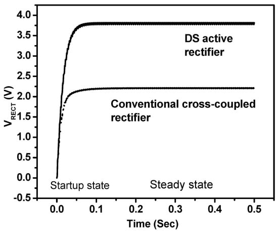
Figure 5.
Comparison of transient voltage at the input of the proposed DS active rectifier and conventional cross-coupled rectifier.
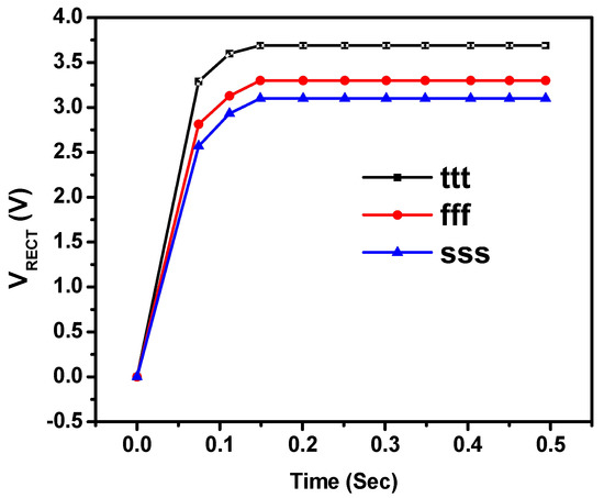
Figure 6.
Proposed DS active rectifier simulations at different corners.
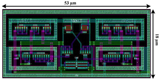
Figure 7.
Layout of the proposed DS active rectifier.

Table 1.
Performance Summary and Comparison of Different Rectifiers.
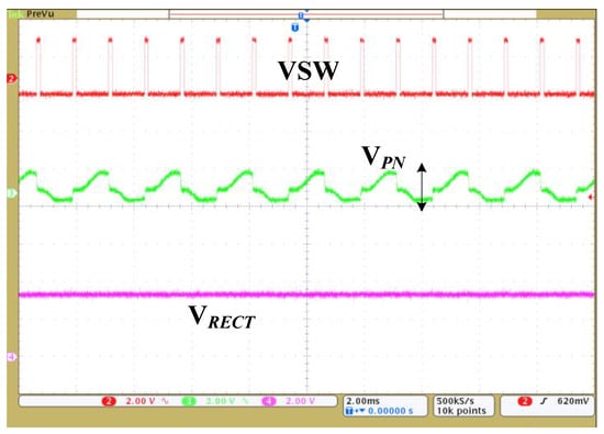
Figure 8.
Measured results of the proposed DS active rectifier.
4. Conclusions
In this research, we show that a dual switch (DS) active rectifier for a piezoelectric (PE) energy scavenging system becomes more efficient by shunting two extra switches with the PE transducer. These switches can significantly increase power extraction from a PE transducer by discharging the transducer capacitor in each half cycle. Moreover, in the proposed dual switch active rectifier configuration, passive diodes are swapped with the comparator-controlled active diodes to minimize the threshold voltage drop . The chip is fabricated using 0.18 m CMOS process with an active area of 53 × 18 mm. The results show that the PCE of 91.5% is achieved. This figure is 4-times more, when it is compared with the conventional full bridge rectifier (FBR) circuit.
Author Contributions
Conceptualization, AU.D. and J.-W.L.; methodology, A.U.D.; software, A.U.D.; validation, J.-W.L., M.K. and W.M.; formal analysis, A.U.D.; investigation, J.-W.L.; resources, J.-W.L., K.A., A.S.A.; data curation, A.U.D.; writing—original draft preparation, A.U.D.; writing—review and editing, K.A., A.S.A.; visualization, M.K.; supervision, J.-W.L.; project administration, A.U.D., J.-W.L.; funding acquisition, J.-W.L., K.A., A.S.A.
Funding
This research was supported by the Basic Science Research Program through the National Research Foundation of Korea (NRF-2018R1A2A2A05018621). The chip fabrication and CAD tools were made available through the IDEC (IC Design Education Center). The authors extend their appreciation to the Deanship of Scientific Research at King Saud University for funding this work through research group No. (RG-1438-034).
Conflicts of Interest
The authors declare no conflict of interest.
References
- Roundy, S. Energy Scavenging for Wireless Sensor Networks with Special Focus on Vibrations; Kluwer Academic Press: Dordrecht, The Netherlands, 2003; pp. 32–58. [Google Scholar]
- Ramadass, Y.K.; Chandrakasan, A.P. An efficient piezoelectric energy harvesting interface circuit using a bias-flip rectifier and shared inductor. IEEE J. Solid State Circuits 2010, 45, 189–204. [Google Scholar] [CrossRef]
- Sun, Y.; Hieu, N.H.; Joeng, C.J.; Lee, S.G. An integrated high-performance active rectifier for piezoelectric vibration energy harvesting system. IEEE Trans. Power Electron. 2012, 27, 623–627. [Google Scholar] [CrossRef]
- Krihely, N.; Ben-Yaakov, S. Self-contained resonant rectifier for piezoelectric sources under variable mechanical excitation. IEEE Trans. Power Electron. 2011, 26, 612–621. [Google Scholar] [CrossRef]
- Lefeuvre, E.; Badel, A.; Richard, C.; Guyomar, D. A comparison between several vibration-powered piezoelectric generators for standalone systems. Sens. Actuators A Phys. 2005, 126, 405–416. [Google Scholar] [CrossRef]
- Lu, S.; Boussaid, F. A highly efficient P-SSHI rectifier for piezoelectric energy harvesting. IEEE Trans. Power Electron. 2015, 30, 5364–5369. [Google Scholar] [CrossRef]
- Umeda, T.; Yoshida, H.; Shuichi, S.; Fujita, F.; Suzuki, T.; Otaka, S.F. A 950-MHz rectifier circuit for sensor network tags with 10-m distance. IEEE J. Solid State Circuits 2006, 1, 35–41. [Google Scholar] [CrossRef]
- Guo, S.; Lee, H. An efficiency-enhanced CMOS rectifier with unbalanced-bias comparators for transcutaneous power high-current implants. IEEE J. Solid State Circuits 2009, 44, 1796–1804. [Google Scholar] [CrossRef]
- Din, A.U.; Chung, D.; Park, D.; Lee, H.; Lee, J.-W. A high extraction self-controllable CMOS resonant rectifier circuit for piezoelectric energy scavenging system. In Proceedings of the 2014 International SoC Design Conference (ISOCC), Jeju, Korea, 3–6 November 2014; pp. 40–41. [Google Scholar]
- Lu, C.; Tsui, C.Y.; Ki, W.H. Vibration energy scavenging system with maximum power tracking for micropower applications. IEEE Trans. Very Large Scale Integr. (VLSI) Syst. 2011, 19, 2109–2119. [Google Scholar] [CrossRef]
- Lu, C.; Tsui, C.Y.; Ki, W.H. Vibration energy scavenging and management for ultra low power applications. In Proceedings of the ACM/IEEE International Symposium on Low Power Electronics and Design (ISLPED), Portland, OR, USA, 27–29 August 2007; pp. 316–321. [Google Scholar]
- Karthikeyan, L.; Amrutur, B. Signal-powered low-drop-diode equivalent circuit for a full-wave bridge rectifier. IEEE Trans. Power Electron. 2012, 27, 4192–4201. [Google Scholar] [CrossRef]
- Lin, H.; Chang, D.K. A Low-Voltage Process Corner Insensitive Subthreshold CMOS Voltage Reference Circuit. In Proceedings of the IEEE International Conference on IC Design and Technology, Padova, Italy, 1–4 May 2006, Padova (ICIDT); pp. 1–4.
- Caliò, R.; Rongala, U.; Camboni, D.; Milazzo, M.; Stefanini, C.; de Petris, G.; Oddo, C. Piezoelectric energy harvesting solutions. Sensors 2014, 14, 4755–4790. [Google Scholar] [CrossRef] [PubMed]
- Dicken, J.; Mitcheson, P.D.; Stoianov, I.; Yeatman, E.M. Power-extraction circuits for piezoelectric energy harvesters in miniature and low-power applications. IEEE Trans. Power Electron. 2012, 27, 4514–4529. [Google Scholar] [CrossRef]
- Lu, S.; Boussaid, F. An inductorless self-controlled rectifier for piezoelectric energy harvesting. Sensors 2015, 15, 29192–29208. [Google Scholar] [CrossRef] [PubMed]
- Do, X.-D.; Nguyen, H.H.; Han, S.K.; Lee, S.-G. A rectifier for piezoelectric energy harvesting system with series synchronized switch harvesting inductor. In Proceedings of the 2013 IEEE Asian Solid-State Circuits Conference (A-SSCC), Singapore, 11–13 November 2013; pp. 10–13. [Google Scholar]
- Kwon, D.; Rincón-Mora, G.A.F. A single-inductor 0.35 μm CMOS energy-investing piezoelectric harvester. IEEE J. Solid State Circuits 2014, 49, 2277–2291. [Google Scholar] [CrossRef]
- Du, S.; Jia, Y.; Seshia, A.A. An efficient inductorless dynamically configured interface circuit for piezoelectric vibration energy harvesting. IEEE Trans. Power Electron. 2017, 32, 3595–3609. [Google Scholar] [CrossRef]
© 2019 by the authors. Licensee MDPI, Basel, Switzerland. This article is an open access article distributed under the terms and conditions of the Creative Commons Attribution (CC BY) license (http://creativecommons.org/licenses/by/4.0/).