Article

Hardware RTOS: Custom Scheduler Implementation Based on Multiple Pipeline Registers and MIPS32 Architecture

by
Ionel Zagan
1,2,* and
Vasile Gheorghiță Găitan
1,2
1
Faculty of Electrical Engineering and Computer Science, Stefan cel Mare University, 720229 Suceava, Romania
2
Integrated Center for Research, Development and Innovation in Advanced Materials, Nanotechnologies, and Distributed Systems for Fabrication and Control (MANSiD), Stefan cel Mare University, 720229 Suceava, Romania
*
Author to whom correspondence should be addressed.
Electronics 2019, 8(2), 211; https://doi.org/10.3390/electronics8020211
Submission received: 8 January 2019 / Revised: 3 February 2019 / Accepted: 12 February 2019 / Published: 14 February 2019
(This article belongs to the Special Issue New Applications and Architectures Based on FPGA/SoC)

Abstract

:
The task context switch operation, the inter-task synchronization and communication mechanisms, as well as the jitter occurred in treating aperiodic events, are crucial factors in implementing real-time operating systems (RTOS). In practice and literature, several solutions can be identified for improving the response speed and performance of real-time systems. Software implementations of RTOS-specific functions can generate significant delays, adversely affecting the deadlines required for certain applications. This paper presents an original implementation of a dedicated processor, based on multiple pipeline registers, and a hardware support for a dynamic scheduler with the following characteristics: performs unitary event management, provides access to architecture shared resources, prioritizes and executes the multiple events expected by the same task. The paper also presents a method through which interrupts are assigned to tasks. Through dedicated instructions, the integrated hardware scheduler implements tasks synchronization with multiple prioritized events, thus ensuring an efficient functioning of the processor in the context of real-time control.

1. Introduction

In the field of Real-time System (RTS), minimizing the jitter when treating the asynchronous events is an important factor in increasing the response speed, this issue being an interesting subject for obtaining fast enough equipment for the most demanding applications. In this regard, in order to guarantee the performance of a RTS, only an increased speed for the execution of tasks does not suffice; an optimal scheduler is also needed in order to meet individual tasks deadlines without reducing their average response time [1,2].
The need to obtain shorter response times to external stimuli for rapid processes has led to in-depth research regarding the processors and RTOS architecture [3]. In this case, most researchers in the field reached the conclusion that some of the components (or even the entire RTOS–HW-RTOS) must be embedded in hardware, due to its capacity to increase the parallel processing of information and, therefore, to decrease response times of the embedded systems [4]. The aim of moving the operating system, or some of its components in hardware, is to reduce the non-determinism sources introduced by external synchronous interrupts and by the variable execution time of the real-time operating system. This variable execution time is determined mainly by the number of tasks, the type of scheduler, data dependency introduced by the assembly line, and interrupts.
Affordable field-programmable gate array (FPGA) devices [5], with a large number of logic gates, can be used as a hardware support for implementing and testing real-time operating systems. With their extensive capabilities for a wide range of applications, the FPGAs are ideal to implement a vast amount of digital logic in a single chip. The main advantages of the programmable logic gate arrays include deep optimization, parallelism, an increased flexibility [6], cost savings and outstanding performances.
The novelty and relevance of the results presented in this paper is given by the nHSE (Hardware Scheduler Engine for n tasks) patented in Germany, Munich [7], as well as through related work publications [8,9]. Based on the multiplication of resources, such as program counter, the pipeline registers and CPU general purpose registers, the nMPRA (multi-pipeline register architecture for n tasks) processor depicted in this paper is based on a minimum response time in treating asynchronous interrupts and events [9,10,11]. Following the validation of the processor using the Virtex-7 development kit [12], Verilog HDL, and the Vivado 2018.2 Design Suite by Xilinx, Inc. (San Jose, CA, USA), the experimental results confirm that context switching operation is performed within a critical RTS timeframe. Considering the nMPRA architecture presented in [11], based on applied research, the following contributions have been made:
  • We proposed a real SoC (System on Chip) implementation of nMPRA and nHSE using the xc7vx485tffg1761-2 FPGA chip (the patent [7] proposes and defines only the architecture with logical gates and flip-flops).
  • In the current implementation we designed the mapping of all nHSE registers in the MIPS32 coprocessor 2 (COP2) register file space, validating the model proposed in patent.
  • We also designed the Verilog HDL implementation of registers and instructions in order to control the dynamic nHSE scheduler (the original project [9] contains only a static round-robin scheduler).
  • We have considered a set of benchmark tests for verifying data hazard and exceptions, for treating asynchronous external interrupts and for inter-task synchronization and communication mechanisms.
The first section of the paper contains a brief introduction, highlighting the contributions of the authors. Section 2 shows a description of the nMPRA processor architecture. Section 3 is dedicated to the integrated hardware scheduler on which the particular results of this processor implementation are based, and Section 4 describes the validation of the proposed nHSE concept, testing the hardware implementation of the inter-task synchronization and communication mechanisms, including the system of handling multiple events. Section 5 compares the results from our nMPRA implementation with other similar projects published in the literature, and Section 6 focuses on discussions regarding the real-time evaluation of the nMPRA processor. The paper ends with the final conclusions in Section 7.

2. nMPRA Architecture

The acronym nMPRA stands for an architecture with multiple (n) pipeline registers. The nMPRA architecture was initially proposed and described in [11], in which a MIPS pipeline [13], the program counter (PC), pipeline registers (PR) and general-purpose registers (GPR) have been multiplied by n times, as shown in Figure 1. Consequently, a structure type PCi, PRi, and GPRi can be defined, so that only a PCi, PRi, and GPRi triad can be activated at a given moment. The result is a structure representing the n-multiplexed resources. Together with the memory and functional blocks (ALU, hazard detection unit, forward unit and the control unit), this structure forms a typical MIPS architecture [14] which we will call semi CPU (sCPU). An i instance of this semiprocessor will be called semiprocessor i (sCPUi). All sCPUis share the same processor units, such as control unit, condition testing unit, hazard detection unit, ALU, and data redirection unit, so that the design of the data path and of the nHSE embedded scheduler must guarantee the consistency of data belonging to different sCPUi. Due to the fact that each sCPUi has a PC, a set of pipeline registers and a GPR, the switch from one sCPUi to another, selected by the nHSE scheduler, does not require any saving of registers and deletion of the pipeline register content [15,16].
If at a certain point, the nHSE deactivates a sCPUi and activates another, all the information specific to the program running on the deactivated sCPUi is preserved due to resources multiplication [17]. The program executed on a sCPUi could be a task, part of a small real-time application. The transition from one sCPUi to another does not require any action in order to save the pipeline register content. This context switching operation generates a very fast switch to a sCPUi scheduled by the nHSE. If every sCPUi runs a task i, then switching from one task to another is very rapid, therefore minimizing the jitter effect produced by interrupts and asynchronous events. In this context each task handles a set of different interrupts (an interrupt can be attached only to a single task at a certain moment).

3. nHSE Unit and Hardware Support

The GPR from the nMPRA processor was specifically designed to achieve a rapid switching of the sCPUi’s contexts, in order to meet the stringent conditions imposed by the real-time systems. The architecture described in this paper does not use the stack concept as in existing processors; however, it uses the functionality of the nested function calls and their order [18], based on the XUM project described in [19]. The scalability of the nMPRA architecture facilitates the convenient organization of n sCPUi’s, in order to dynamically or statically schedule a reasonable number of tasks. Because the nHSE scheduler implements a preemptive scheduling algorithm based on priorities, the architecture proposed in the present paper fully meets the requirements of applications for monitoring and controlling industrial processes. Thus, the interrupts can be attached to the sCPUis with a higher or a lower priority and their asynchronous activation would not alter the feasibility of scheduling the set of tasks.
If the periodic execution of a task is needed, as in the case of managing the human machine interface (HMI), or that of collecting data from sensors, the timers implemented at the level of each sCPUi can play a very important role in the structure of such a system. Under these circumstances, the robustness of the CPU results from the outstanding performances obtained from context switching, from handling external interrupts, and from the simplicity of the architecture.
Figure 2 shows the nHSE scheduler module designed at the level of COP2. The events treated by the nHSE scheduler are the following: the timer-generated event (TEvi), the event produced by overcoming the first critical limit (D1Evi), the event produced by overcoming the second decisive limit (D1Evi), the event produced by the watchdog timer (WDEvi), interrupts (IntEvi), inter-task communication mechanism (SynEvi), and the mutex-generated events (MutexEvi).

3.1. Command, Control, and Status Registers of the nMPRA Concept with Direct and Indirect Effect over the nHSE

MIPS provides the user with a system of coprocessors for extending the functionality of the basic CPU. Coprocessor 2 is available to the user. The nHSE architecture contains four types of registers:
  • Monitoring registers (mr_)—can be accessed only by the sCPU0 and possibly by the monitored sCPUi.
  • Control registers (cr_)—specific to each sCPUi.
  • Local registers (lr_)—private space of each sCPUi.
  • Global registers (gr_)—can be accessed by all sCPUi.
The presence of new registers requires also the extension of the MIPS32 instruction set. The COP2 instructions are generic and, according to their implementation, they can have other mnemonics or also can be implemented using macros. As can be seen in Figure 3, the multiplication of resources for 4 sCPUi is represented by the ID_Instruction_reg[3:0] pipeline registers. With the Vivado simulator, we can observe the control and monitoring registers designed at the level of the nHSE module. Through the nHSE_Task_Select (ID_sCPUi) and nHSE_EN_sCPUi (en_sCPU0/en_sCPUn−1) signals, the hardware scheduler module dictates the execution state for all sCPUi, and the nHSE_inhibit_CC signal can inhibit context switching in certain critical situations.

3.2. Implementing the Instructions Dedicated to the nHSE Embedded Scheduler

This implementation represents an example of a generic nHSE-type correspondence MIPS coprocessor with two instructions. Other processor implementations can perform other correspondences, depending on the application. Thus, data transfer between nHSE and COP0 is achieved by using four instructions implemented at the level of COP2, namely CFC2 (copy control word from coprocessor 2), CTC2 (copy control word to coprocessor 2), MFC2 (move word from coprocessor 2), and MTC2 (move word to coprocessor 2). The new instructions presented in Table 1 have been designed using the MIPS32 Release 1 ISA, the significance of the registers being explained in detail in the specifications of the nMPRA processor. We have improved the patented nMPRA concept, removing the multiplication of the register file for each function call, because this involves high resource consumption.
The time required for switching contexts is the key element of this hardware scheduler. The nMPRA concept uses a unified space for interrupts and tasks and, therefore, interrupts inherit the priority and the characteristics of the tasks to which they are attached [20]. Thus, contexts switching takes place within a clock cycle, depending on the moment of the event threated by nHSE. At the same time, the task can respond to an external event, if that event is masked by the wait Rj instruction with movcr mnemonic. This instruction is very important because it allows the synchronization of execution when multiple events are to be expected.
The execution of the wait Rj instruction by COP2 results in copying the content of the Rj register (COP0) in the crTRi register (COP2) of the nHSE scheduler, in order to validate the events expected by task i attached to the sCPUi. If at least one of the events is active, its value is copied in the Rj. The action of the wait Rj instruction for a semiprocessor i is crTRiRj, where Rj represents a general purpose register GPR[rt] at the level of COP0, and crTRi is a register intended to validate or inhibit one of the seven events.
Table 2 lists the specialized task manipulation functions implemented by the nHSE unit. Switching from one state to another can be performed either through the task managing functions (wait Rj), or by the nHSE scheduler in the presence of validated events at the level of each sCPUi. These instructions enable the activation/deactivation of a task. The wait instruction enables the creation/inhibition of one or more periodic or aperiodic events at the level of each sCPUi. This way, the registers corresponding to each sCPUi in the Data Registers Bank (Figure 2) memory area of the nHSE (activated/inhibited events) are accessed. If at least one event is active at the time of the call, the task is not preempted. Otherwise, the current task is suspended (Preempts) and the scheduler dispatches the next task to execute, putting it on the running state. The block diagram in Figure 2 shows the Configuration Registers Banks implemented in nHSE that makes possible to access the monitoring registers of each task, i.e., the sCPUi, by the means of the RWsCPUiState instruction (Table 2).
Before activating the task, the parameters corresponding to each task must be set through the CTC2 and MTC2 MIPS32 instructions (Table 1), taking into account the priority of the tasks and the RTS requirements. It should be specified that the implementation of instructions, such as the Create/Destroy Task was not necessary, because each task running on the sCPUi has its own context due to the resources multiplication on which the nMPRA concept is based. The last two instructions (sCPUiswEv and sCPUiswExc) enable the software to alter the state of an event treated by a certain sCPUi, and the sCPUiswExc instruction generates a software exception (Table 2).
Figure 4 shows the supported task states and the corresponding transitions between them. There are also the conventional task states, such as stopped, idle, ready, running, preempted, and blocked. For conceptual considerations of the nMPRA architecture, the free and sleeping state have not been implemented.

4. Implementation and Validation of the nMPRA Architecture

4.1. Management of the Events and Interrupts with Support of Dynamic nHSE Embedded Scheduler

The crTRi, crEVi, and crEPRi control registers (Table 1) validate, store, and prioritize the events and interrupts expected by each sCPUi. With an independent execution, the scheduler has entries for multiple events prioritized differently by each sCPUi through the crEPRi (event priority register) control register. In order to store each event treated at the level of a sCPUi, gr_EV_select_sCPU[3:0] global registers have been used, with values from 0 to 6, depending on the treated event; 7 indicates the fact that there is no active event. The mrPRIsCPUi[3:0] registers provides the priority of each sCPUi, which can only be modified by the sCPU0. 
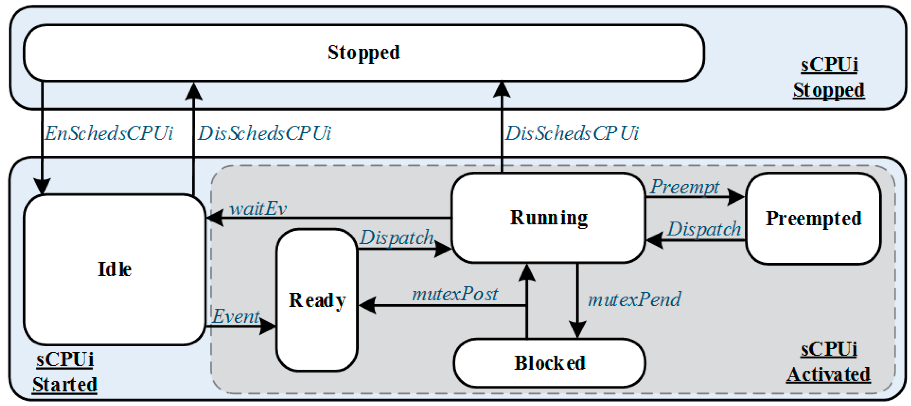
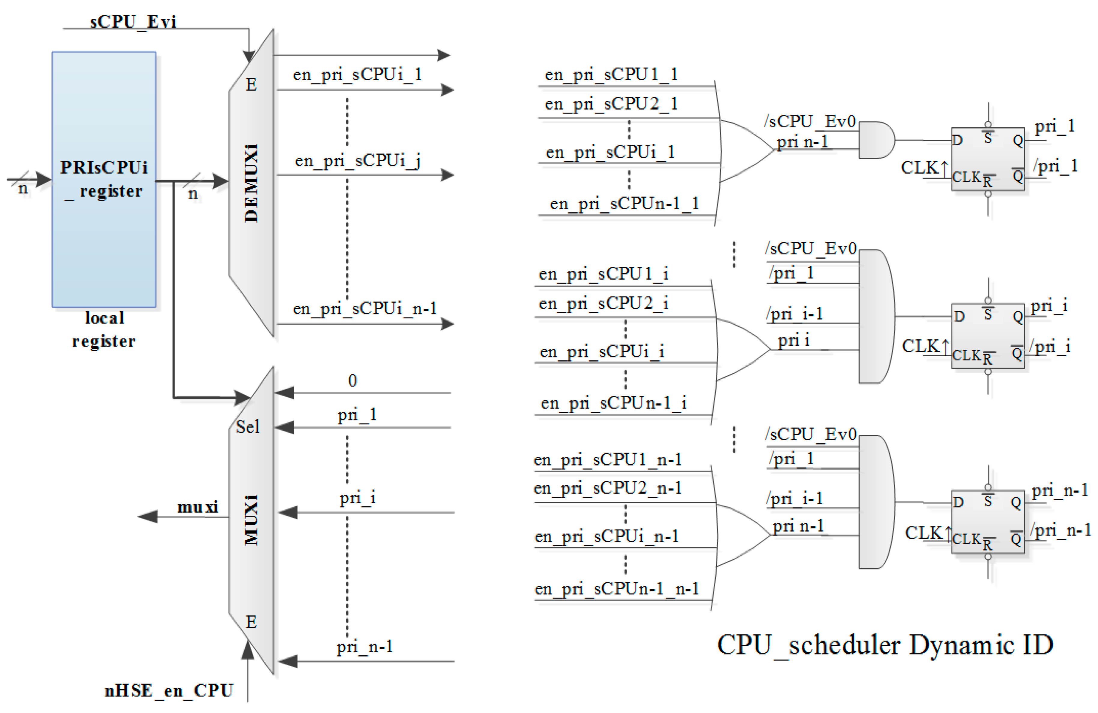
Figure 5 shows the support for the dynamic scheduler. For each sCPUi a local register is provided, enabling the writing of the desired priority at a given moment. An exception to this rule is sCPU0 which always has 0 priority (the highest).
Based on the value stored in the mrPRIsCPUi register, which can be from 1 to n − 1 (without 0), sCPU_Evi and nHSE_EN_sCPUi signals, the pri_1/pri_n − 1 signals are generated; in turn, these signals generate the muxi signal. The sCPU_Ev0, mux1, mux2, …, muxi, …, muxn-1 signals are used to generate the task ID in a similar manner like it was generated for the static scheduler. In fact, the same coder is used for the static ID, the correspondence being sCPU0_ready with sCPU_Ev0, sCPU1_ready with mux1, sCPU2_ready with mux2, sCPUi_ready with muxi, sCPUn-1_ready with muxn-1 respectively.
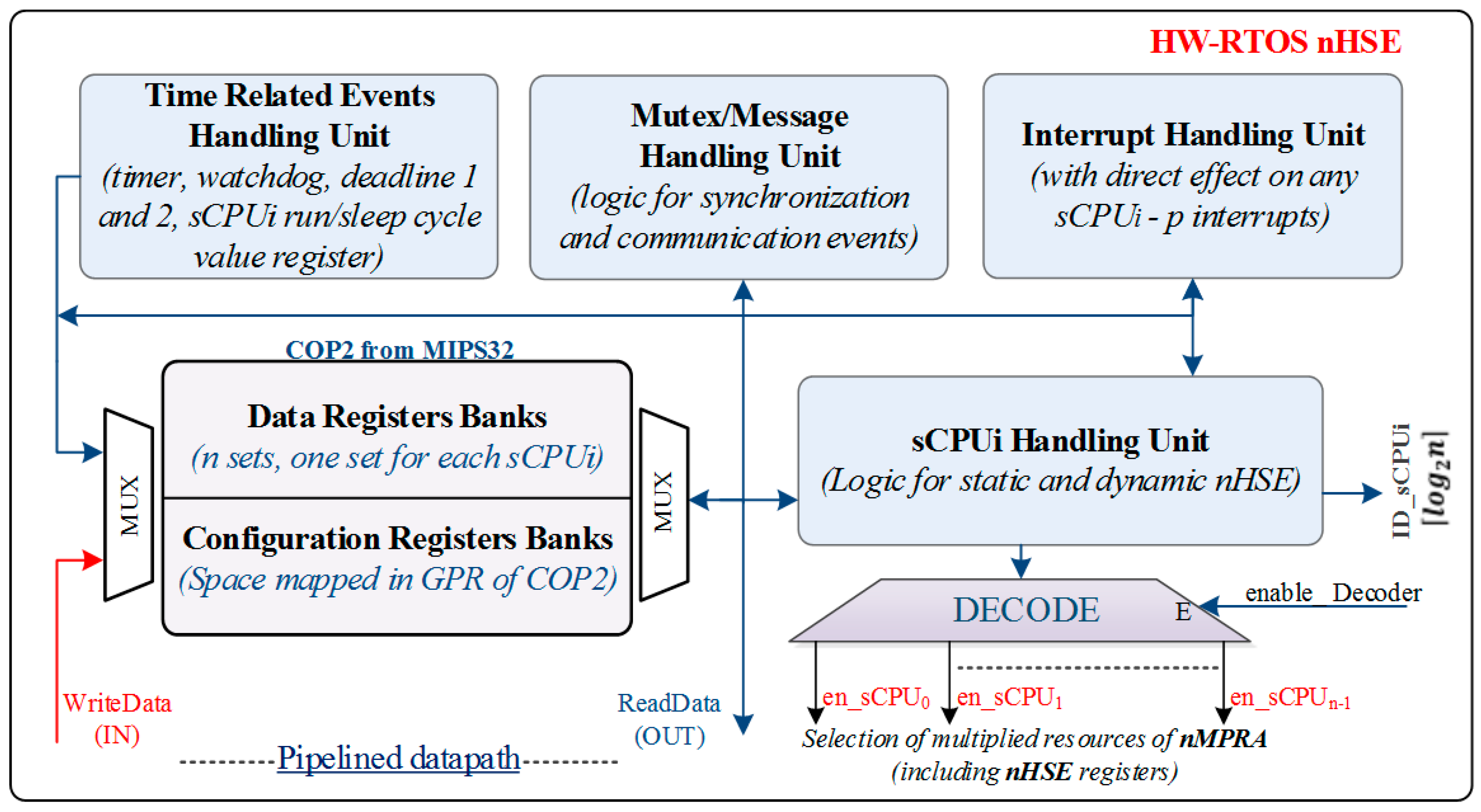
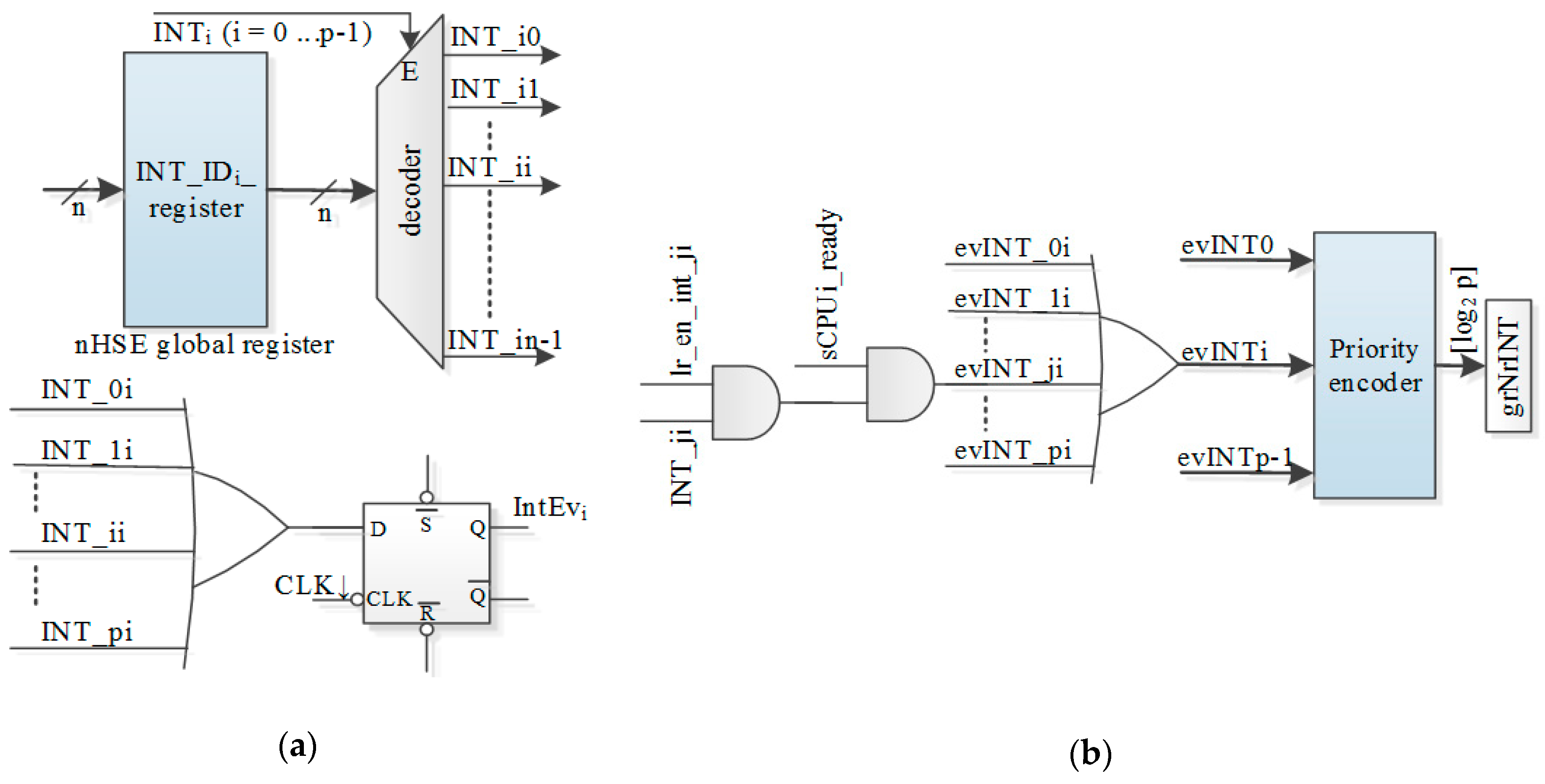
Figure 6a presents the scheme proposed for the interrupt events. We assume that there are p interrupts in the system. For each interrupt, there is a global register with n useful bits and a INT_IDi_register that stores the ID of the task to which the interrupt is associated. The activation of the INTi interrupt validates the decoder Decoder which, in turn, activates one of the INT_i0INT_in-1 signals.
The gate OR (Figure 6a) can collect all interrupts from the system. They can be attached to sCPUi if all p INT_IDi_register (i = 0…p-1) registers are written with the i value. Correspondingly, no interrupt can be attached, if none of the p INT_IDi_register (i = 0…p – 1) registers are written with an i value. The D type bistable has the role of synchronizing the random occurrence of the INTi interrupt event, generating the IntEvi event. The HW-RTOS scheduler automatically detects that a high priority task (sCPUi) is waiting for this interrupt and thus makes the task ready-to-run.
A deficiency of the priority encoding scheme is that when a task has multiple interrupts attached to it, a loop testing is executed when the prioritization is performed through software, and the response time depends on the position in the loop.
The proposed scheme is very versatile and can implement many interrupt working models in a real-time executive, Figure 6b presenting a real improvement in this context. If all interrupts were attached to a single task, the interrupt with the highest priority would be INT0, and the interrupts with the lowest priority would be INTp-1. From this point of view, the priorities are fixed. In order to take into consideration only the interrupts of a single task, with the highest priority at a given moment, the local registers crEPIji (one of the local registers for validating the interrupts for their priority encoder) were considered (j is sCPUj, i is the register number). These registers contain one bit for each of the p interrupts. If the bit is 1, the interrupt is attached to the task and the INT_IDi register must be written with the task ID. This correspondence must be ensured for any interrupt attached to a task. If this correspondence does not occur for an interrupt, the interrupt will never generate an interrupt code because an evINT_ji signal will always be 0 logic. The evINT_ji signal will activate only if the sCPUj, to which it was attached, is in execution corresponding to the sCPUj_ready signal on 1 logic. For example, the evINTi signal can collect all possible i interrupts attached to any sCPUi’s, but it is mandatory that an interrupt is attached to a single task (sCPUj). Consequently, since only one sCPUj is active at a given moment on the input of the priority encoder, only the interrupts of that task can be active. Using the grNrINT register, sCPUj will read the number of the highest priority event.
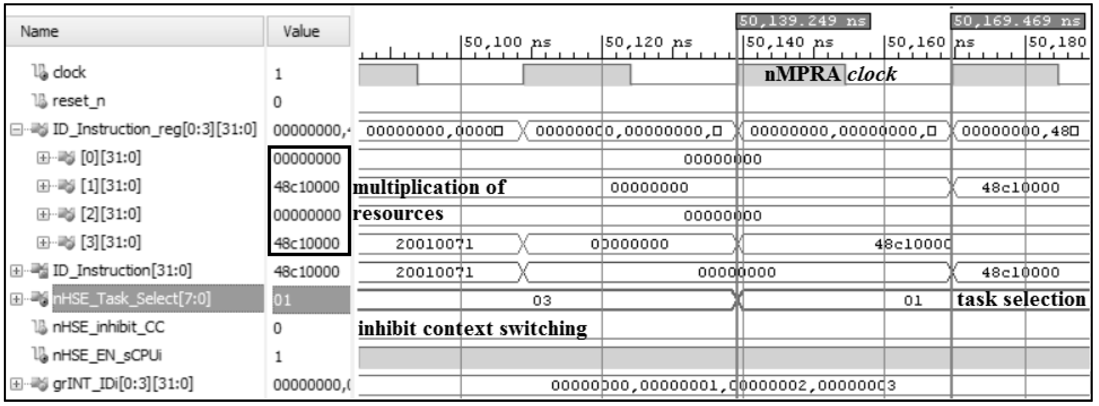
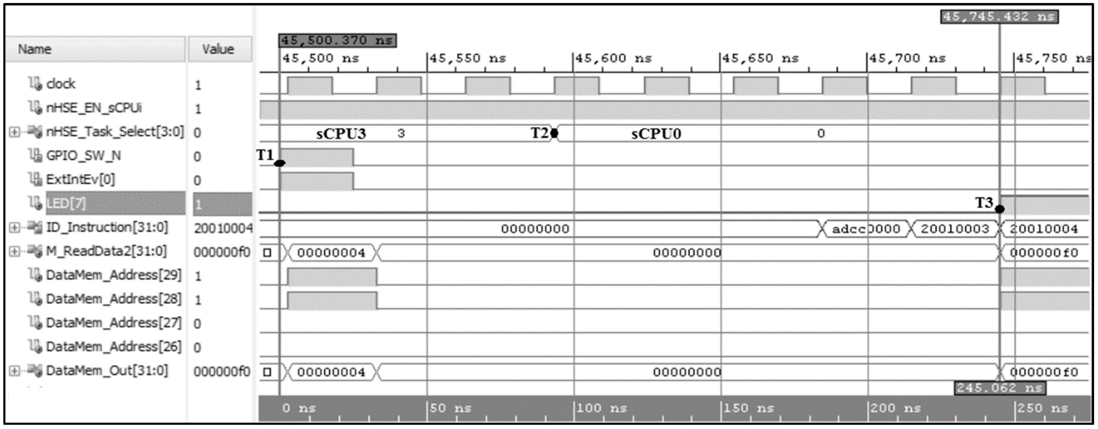
The response time of the nMPRA processor can be simulated and measured when an asynchronous external event occurs; the time required to switch contexts can also be determined. Simulation waveforms with Vivado illustrate the internal signals of the processor at the working frequency of 33 MHz, GPIO_SW_N representing the input signal assigned to the ExtIntEv[0] interrupt event (pushbutton), marked by time moment T1 (Figure 7). Therefore, to treat this external interrupt attached to sCPU0, about three clock cycles are sufficient (T1–T2 time period). The time moment T2 indicates the response of the nHSE scheduler by modifying the nHSE_Task_Select internal signals to execute sCPU0. Time moment T3 indicates the change of the LED[7] signal state (Figure 7) and the corresponding output of this LED is mapped in the data memory address space. In order to access this led, the processor will run a sw type MIPS instruction (0xadcc0000). From the occurrence of the external event, until the LED on the Virtex-7 is switched ON, up to eight clock cycles are required (245.062 ns), depending on the moment T1 when GPIO_SW_N pushbutton is activated.
For treating multiple events with their own trap cells (interrupts, mutexes and message events), the proposed solution integrates the priority encoder for interrupts, on the one hand, and for local events associated to a sCPUi, on the other. This way, the scheduler provides hardware support for an automatic jump to the handler, treating the event with the highest priority assigned to the semiprocessor sCPUi. In software operating systems, the operation of saving and eventually restoring the current task contexts inserts significantly longer delay times (from a few us to tens of us), and it increases the degree of unpredictability generated by various search operations in lists or tables based on the task identifier.

4.2. Inter-Task Synchronization and Communication Mechanisms

Two other fundamental aspects, distinctive to the nMPRA concept are the mechanisms of synchronization and communication. This is an interesting research topic and is related to the sharing of resources by the nMPRA processor tasks. The integration of these mechanisms in hardware conveniently improves the worst-case execution time (WCET), thus providing an optimal solution for communication between tasks and mutual exclusion in the case of shared resources. From an architectural standpoint, these mechanisms must introduce extremely brief critical code sections corresponding to certain atomic operations. In other words, the implementation of mutexes is based on atomic instructions, achieving good performance, and short CPU blocking times.
Table 3 shows the working instructions for mutexes and the communication mechanism through messages implemented at the level of the nHSE module. Mutex and message type events are created through the CTC2 and MTC2 MIPS32 instructions (Table 1). The mutexPend, mutexPost, mutexAccept, and msgSent functions are fully or partially implemented in hardware using MIPS32 LWC2 and SWC2 instructions. Therefore, the validation of multiple events, such as mutex or message, can be signaled by the dedicated wait Rj instruction.
The hardware support for implementing the synchronization mechanism is Mutex Regiter File (MRF) and the associative search of a mutex release is done based on a Content Addressable Memory (CAM) principle. These grMutexi special registers, which compose the MRF, contain the mutex status and the owner task ID. The number of mutexes (we used m as an example) depends on the application. Sharing resources by all sCPUi’s in nMPRA implies that the grMutexi global registers can be accessed by any sCPUi under the direct control of the nHSE scheduler. Regarding the real-time aspect, it is fundamental to avoid suspending execution when a mutex is modified, as the operations with these entities are atomic. As soon as the mutex or the expected message is unlocked or received, the suspended task is reactivated by the nHSE, entered into the Ready state and executed according to its priority. Every grMutexi register contains a bit for storing the state of the mutex and m-1 bits for storing the owner sCPUi ID. When a task i running on the sCPUi semiprocessor receives a message or expects the release of a mutex, it is necessary to identify the source of the event.
Being accessed by all sCPUis, the mutex lock and release operations must be performed indivisibly with the help of nHSE_inhibit_CC signal. When the Mutex_i bit is 0, it is considered that the mutex i is available, a sCPUi being able to lock only one mutex at a certain time. Since these mechanisms are implemented in hardware, the time needed to search the message source or the selection of a sCPUi that is expecting a mutex can be performed in a time period characteristic to real-time systems. Table 4 describes the MIPS code of a benchmark test to evaluate the synchronization mechanism presented in Figure 8. In the example illustrated in Figure 8, the crEMRi0 = 0x0000000F and crEERi0 = 0x0000000F registers (Table 1) indicate the fact that four mutexes and four inter-task communication events are validated. It should be emphasized that these registers have the role of validating the synchronization and communication mechanisms and cannot produce MutexEvi or SynEvi events. Next we illustrate the situation where the scheduler waits to deactivate the nHSE_inhibit_CC signal, delaying the response of the nHSE scheduler. Therefore, it is possible to analyze the contents of the COP2 registers when a context switch is performed concurrently with the occurrence of a mutex event (T1). As we can see, context switching performed at time moment T2 to treats the mutex event requires one clock cycle. When the mutex (MutexEvi event) is signaled, the HW-RTOS automatically determines whether a sCPUi is waiting for the signal and if so, initiates a context switch to the waiting task based on sCPUi priorities.
In order to implement the inter-task communication mechanism, the nMPRA architecture uses a number of grERFi global registers, each of 2n+k+1 bits. These registers compose the Events Register File (ERF), each register using a bit to store the event status, 2nj bits to store the their tasks ID, source, and destination, and k bits to store the message. Therefore, grERFi is the register that defines an event, and is part of the ERF; after a reset, all bits are 0. The source and destination identifiers have nj bits, where n represents the ID of the sCPUis.
The oscilloscope capture in Figure 9a illustrates the results of the response time measurement when treating an asynchronous external event attached to sCPU0 semiprocessor. Thus, the presented signals validate the nHSE scheduler by practically checking the waveforms in Figure 7. There can be a 30.3 ns jitter, depending on the moment when the interrupt occurred and the next rising edge of the clock cycle (nMPRA clock = 33 MHz). The trigger of the input signal generated by the GPIO_SW_N pushbutton is at the time moment T1 = −2.575 ns, and the reaction of the semiprocessor sCPU0, by switching ON the LED[7] on the Virtex-7 kit, occurs at time moment T2 = 266.0 ns. The response time, obtained by using the PicoScope 2205MSO oscilloscope by Pico Technology (St Neots, UK), is only of Δt = 268.6 ns (Figure 9a); this validates the real-time characteristic of the nMPRA architecture and checks the WCET coefficients in Table 8.
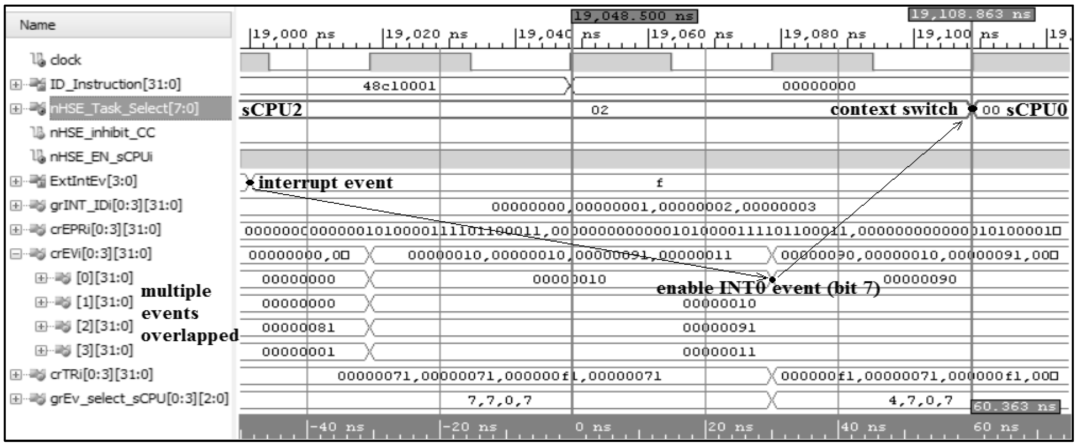
Figure 9b presents the jitter of the application running on nMPRA in order to test the communication mechanism. Since the CAM search in the grERFi registers is performed in hardware, the jump to the trap cell assigned to message events is done in only two clock cycles, sCPU0 having the highest priority in the system. As can be seen in Figure 10, in order to simulate the standard deviation of the response time, multiple overlapped events attached to sCPU0 and sCPU2 were considered. The crEPRi[i] registers presented in Figure 10, represents the priorities attached to each event that can be validated or not at the level of each sCPUi. Thus, at the level of sCPU0 (mrPRIsCPUi[0] = 0x00000000) the interrupt event has the highest priority (crEPR0[14:12] = 000), with no other events waiting to be executed for that moment. If a sCPUi has more validated events, the jitter increase according to the priority of the enabled events.

4.3. The Impact of Different Configuration Models on FPGA Resources and Energy Consumption

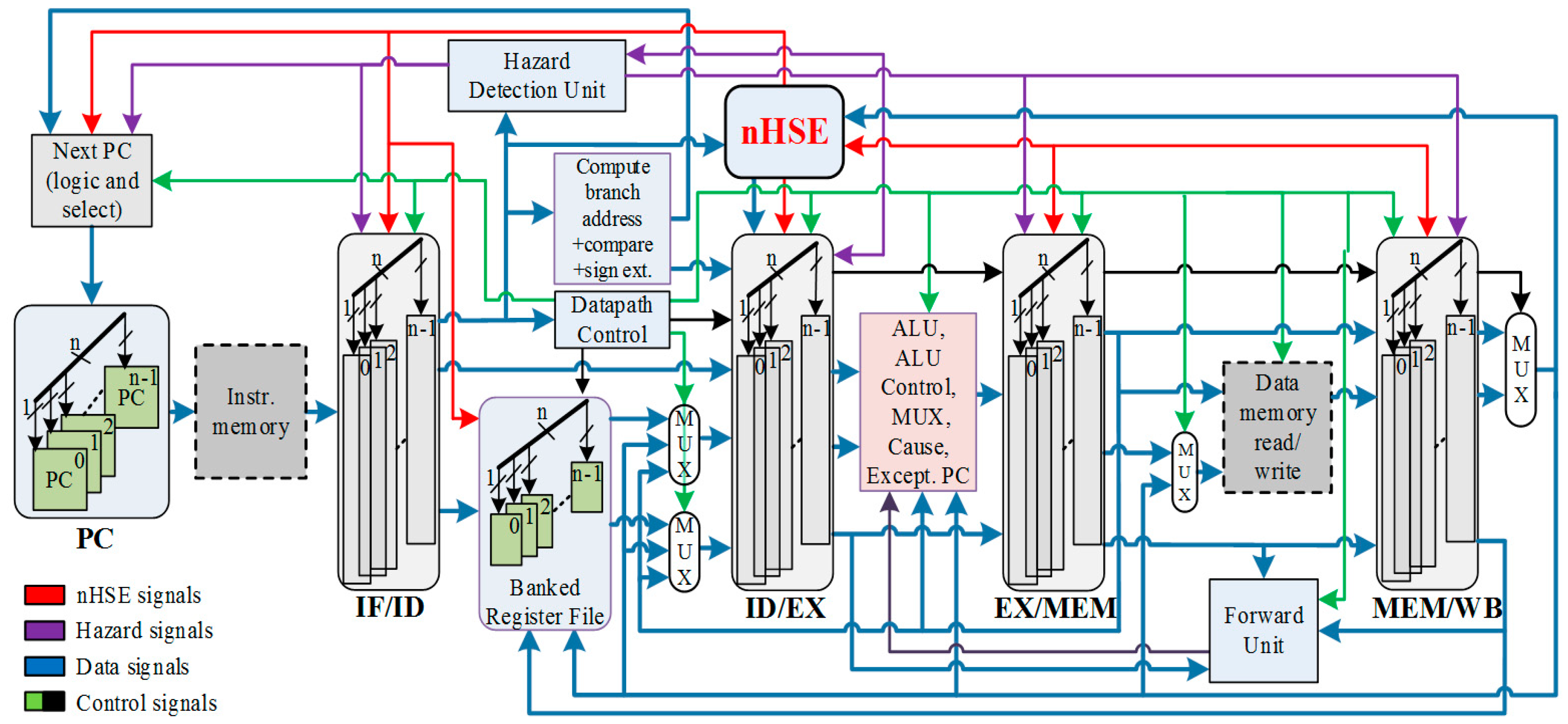
Although nMPRA is a resource multiplexing architecture, its implementation is more cost effective compared to other architectures proposed in the literature. It should be specified that such an implementation has significant advantages over the existing commercial implementations for a number of 16, 32, or even 64 tasks. Implementing this architecture for a large number of tasks would entail too many resources related to the system in which the processor is used, and unwarranted large signal propagation times, significantly reducing the processor’s working frequency. Since the multiplexing resource multiplication operation was performed at the level of each memory element, the cost/performance ratio obtained was more than convenient. Therefore, only the multiplication of the registers contained in the ID/EX pipeline stage was performed, and not the multiplication of the whole ID/EX module, thus gaining a significant advantage over other implementations. The modules containing only combinational elements, such as the Hazard Detection module, have not been multiplied because they provide output signals corresponding to the inputs, these values being already stored in the nMPRA registers.
Table 5 illustrates the logic blocks requirements for implementing the nMPRA architecture with various sCPUi, mutexes (grMutexi) and message events (grERFi), where i = 4, 8, and 16, including the resources needed to implement the nHSE scheduler, the recent version being greatly improved than the one described in [11,21]. Therefore, in designing the nHSE module, the number of sCPUis, inter-task synchronization events, and the number of external interrupts are firstly taken into account. The scheduler must contain all the memory elements needed by the above-mentioned entities, as well as the combinational logic necessary to ensure the correct operation of the static and dynamic scheduler, even when exceptions occur. The number of sCPUi that nHSE controls through the generated signals is the key factor in determining the resource requirement for implementing the nMPRA architecture.
Table 6 presents the resource requirements for implementing the entire SoC project that includes the nMPRA processor. It is worth mentioning that these requirements include the resources used for the on-chip implementation of the dual-port memory for instructions and data, the resources needed for implementing the HMI, and the UART communication for writing the program memory and implementing the oversampling mechanism for the input data of the UART module.
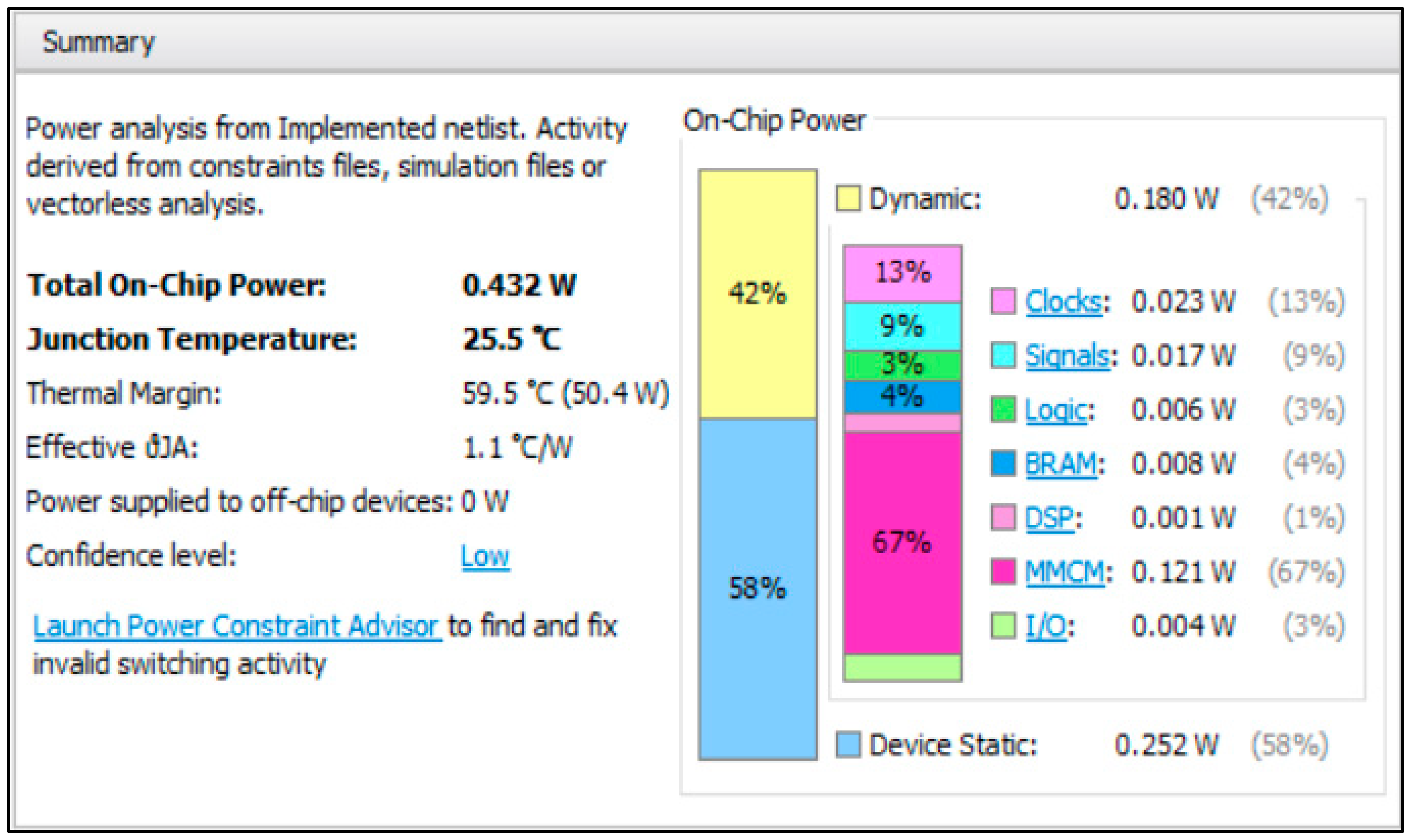
Figure 11 shows, in details, the power consumed by the nMPRA implementations, with eight sCPUi, eight grMutexi, and eight grERFi, based on the hardware support for treating interrupts, their dynamic attachment to any sCPUi, and the hardware implementation of the inter-task synchronization and communication mechanisms.
The different values presented in Figure 11, depending on the nHSE module and xc7vx485tffg1761-2 FPGA used for implementation, were obtained following the practical implementation of the nMPRA processor using the Vivado 2018.2 Design Suite and the Virtex-7 development kit by Xilinx, Inc. (San Jose, CA, USA). However, the overall power consumption is more than acceptable compared to other similar implementations [22,23].
The implementation in hardware of the nHSE scheduler and of the synchronization and communication events guarantees the predictability for the task set and the deadline set in the boot and initialization sections. The results have been obtained using an nMPRA processor with working frequency of 33 MHz, which can be increased by the improvement of the instructions and data memory used.

5. Related Work

An interesting challenge is proposed by Edwards and Lee in [24]. They believe it is time for a change in the architecture of real-time systems, which ignores the predictability and repeatability of temporal features. Thus, as a solution, [25] presents a new processor architecture with a behavior in time that is as easy to control as its logical functions. These processors are called Precision Timed Machines—PRET. For this new processor architecture, there are a lot of challenges related to programming languages, memory hierarchy, cache, virtual memory, pipeline techniques, power consumption management, I/O and DRAM design, bus architecture, just-in-time compilation (JIT), multitasking, task scheduling, and software component technologies.
The FlexPRET project presented in [26] is a fine grained multithreading processor. This implementation has been designed to also support architectural techniques for mixed criticality systems. The architecture proposed by the authors supports the interlacing of an arbitrary number of controlled threads by a new scheduler. The threads are classified as hard (hard real-time thread - HRTT) and soft (soft real-time thread—SRTT). FlexPRET supports the hardware isolation for HRTT, enabling at the same time the SRTT threads to efficiently use the processor. Therefore, the dynamic scheduler introduces the advantage of using all processor cycles at the expense of a WCET being more difficult to obtain.
The Merasa project [27,28] has been developed in order to obtain a processor architecture which is successfully used for the hard real-time systems. The MERASA project has a mixed criticality oriented hardware system, focusing on the multi-core level [27]. The main characteristics of this project are task execution predictability and the efficient analysis of the WCET coefficient for each task. The proposed architecture is based on the simultaneous multithreading (SMT) technique, and is able to simultaneously execute both hard real-time (HRT) and non-real-time (NHRT) execution threads. In order to manage the shared resources and critical execution thread sections, the proposed architecture provides inter-task synchronization and communication mechanisms, such as spin-lock, conditional variables or barriers.
The MicroBlaze processor [29] is a FPGA-optimized 32-bit RISC soft processor, with virtual memory management, 32-bit general purpose registers, cache software support, and AXI4-Stream interfaces. For an optimal configuration of the MicroBlaze processor, Xilinx provides the Configuration Wizard tool. This option is used successfully with various FPGAs. The MicroBlaze core resource utilization for various parameter configurations perfectly matches to the predefined templates in the MicroBlaze Configuration Wizard.
The ARPA-MT processor provides several permanent execution contexts in hardware [30], the IF and ID replication of the pipeline registers for each instanced task, and runs concurrently on the last three pipeline stages (EX, MA, and WB). The solution of replicating the resources containing the architectural state of tasks is an expensive hardware one. However, ARPA-MT processor improves the efficiency and determinism of the system management functions and services, minimizes the task switching speed, and reduces the number of task context switches.
In [31] the authors propose a hardware scheduler based on task queues. In order to meet the stringent conditions imposed by the RTS, this scheduler improves the system performances in exchange for the inflexibility, integration difficulties and for increasing the hardware resources used by the FPGA. The proposed hardware scheduler can be configured to support various algorithms such as earliest deadline first, time sliced priority scheduling and least slack time. Following the experimental results for both periodic and aperiodic tasks, the authors argue that the hardware scheduler can significantly reduce the event trigger latency, from 8518 (software eCos) to 1424 clock cycles (using eight tasks). Therefore, the hardware scheduler proposed reduces the overhead generated by the scheduler by more than 1000 clock cycles and raises the system utilization bound by a maximum 19.2%. Although it adds an additional resource cost of around 17% of a typical softcore system, the scheduling jitter is reduced from a few hundred clock cycles, when this operation is performed in software, to only two or three clock cycles for most operations. The authors assert that the proposed configurable scheduler architecture can achieve outstanding performances because it operates in parallel to the processor and requires no system tick ISR (Interrupt Service Routine) when compared to a software scheduler. However, the new task queue scheduling model can reduce drastically the operating frequency as the queue depth increases the queue limit in order to not introduce this negative effect of up to 64 levels.
In [32], the authors propose a real-time management of hardware and software tasks for embedded FPGA-based systems. Considering that real-time systems are subject to dynamic workloads and have tasks that can be computationally intensive, this paper introduces a novel resource allocation scheme and an online admission control test that achieves high performance and flexibility. However, the system uses a runtime reconfiguration to maximize the number of admitted real-time tasks. The results of simulations performed using a set of tasks show that the performance benefits of relocation have been successfully measured and underlined. Studying this paper, we can assert that the online task assignment and migration between the processor and the reconfigurable device are detailed, obtained for both commonly used slotted and 1D area models.
Table 7 presents a comparison between the nMPRA architecture and a few other processor implementations. The authors of the present paper aimed a realistic comparison between these different implementations by using different designing platforms. Regarding the experimental data presented in Table 7, nMPRA and MicroBlaze implementation was tested by the authors whereas for the remaining solutions we took the values reported by the authors of the referenced papers.

6. nMPRA Evaluation Relative to Periodic Real-Time Executive Overhead and Discussions

In order to determine the impact of the nHSE scheduler on the execution of real-time applications over nMPRA executive, several parameters have been evaluated. It has mainly been taken into consideration the improvement of three parameters, namely the time for the selection and treatment of multiple events, the time required for task context switching, and the software overhead of several internal functions and application services.
Table 8 presents the WCET coefficients in microseconds following the processor performance evaluation presented in this paper. For this, a set of four tasks that passed the feasibility tests have been used, each with multiple periodic and aperiodic events attached, and with imposed relative deadlines. The following times have been measured: the relative time for the initialization and boot operation of the real-time executive, the time required for the task context switching operation in the least favorable case when the assembly line contains atomic instructions, and the task activation time by an interrupt or the selection of an aperiodic event. Following the execution of the inter-task synchronization and communication mechanisms described and validated in Section 4, the results obtained by the nHSE scheduler are significantly better than the existing proposed scheduling architectures which use tens or even hundreds of clock cycles. The results of the experiments, obtained following the implementation and validation of the nMPRA processor, have shown a minimum WCET. This is because the combinational part related to the scheduling and configuration operation is performed in hardware, in parallel with the execution of the user application, and not contributing to the computational overhead of the RTOS. In most conditions, the HW-RTOS responds faster than its equivalent software-based operation. The following aspects contributed to the WCET coefficients obtained and presented in Table 8: the multiplication of resources for each sCPUi in nMPRA, the hardware implementation of the nHSE scheduler at the level of COP2, as well as designing the synchronization and communication mechanisms as part of the nHSE module.

7. Conclusions

The robustness and performance of the nMPRA architecture is guaranteed by the context switch operations, presence of the inter-task synchronization and communication mechanisms and the efficient use of multiplexed resources by designing in hardware the real-time nHSE scheduler. The interrupt prioritization scheme has also been extended over events, thus becoming a hardware solution for a new event attached to any sCPUi for treating the situation when multiple events become active. The round-robin or preemptive scheduling scheme, that can be implemented by the nMPRA module with the help of integrated timers and hardware activated tasks, meets the AutosarOS requirements that inherits the OSEK/VDX characteristics. By using the nMPRA architecture in the project segment of this field, and by implementing the context isolation in accordance with ISO26262, a requirement proposed for implementation starting with the 4.0.3 version of the Autosar standard, additional performance can be achieved. It is a realistic idea because the multiplication of resources in the nMPRA processor does not entail a significant cost related to the available resources. Increasing safety in such systems is just one of the main important features of this concept.
The nMPRA architecture and nHSE scheduler also supports the configuration of the task number with flexible priority levels. The proposed architecture allows high performance inter-task synchronization and communication mechanisms, improving the overall response time when the mutex or message is expected for a higher priority task. Since it is a configurable scheduler, nHSE enables designers to more efficiently utilize the processor time and tune the task set parameters to reach maximum performance for the applied applications.

8. Patents

The nMPRA and nHSE concept presented in this paper is patented in Germany, Munich (DE202012104250U1) [7].

Author Contributions

Conceptualization: I.Z. and V.G.G.; software: I.Z.; data curation: I.Z.; writing—original draft preparation: I.Z. and V.G.G.; writing—review and editing: I.Z. and V.G.G.; supervision: V.G.G.; project administration: I.Z. and V.G.G.; funding acquisition: V.G.G.

Funding

This research was funded by the project “Demonstrator experimental de laborator bazat pe nHSE - sistem de operare de timp real integrat în hardware - implementat pe o arhitectură ZScale - RISC V”, acronym: nHSE-RiscV, contract no. 219PED/2017, PN-III-P2-2.1-PED-2016-1460, PNCDI III, using the infrastructure from the project “Integrated Center for research, development and innovation in Advanced Materials, Nanotechnologies, and Distributed Systems for fabrication and control”, contract no. 671/09.04.2015, Sectoral Operational Program for Increase of the Economic Competitiveness co-funded from the European Regional Development Fund.

Acknowledgments

The authors would like to thank the editor and the anonymous reviewers for their valuable comments and suggestions that improved the quality of this paper.

Conflicts of Interest

The authors declare no conflict of interest.

References

  1. Koulamas, C.; Lazarescu, M.T. Real-time embedded systems: Present and future. MDPI Electron. 2018, 7, 205. [Google Scholar] [CrossRef]
  2. Wang, W.; Zhang, X.; Hao, Q.; Zhang, Z.; Xu, B.; Dong, H.; Xia, T.; Wang, X. Hardware-enhanced protection for the runtime data security in embedded systems. MDPI Electronics 2019, 8, 52. [Google Scholar] [CrossRef]
  3. Zagan, I.; Găitan, V.G. Improving the performances of the nMPRA processor using a custom interrupt management scheduling policy. Adv. Electr. Comput. Eng. 2016, 16, 45–50. [Google Scholar] [CrossRef]
  4. Lee, J.; Mooney, V.J.; Daleby, A.; Ingstrom, K.; Klevin, T.; Lindh, L. A comparison of the RTU hardware RTOS with a hardware/software RTOS. In Proceedings of the Asia and South Pacific Design Automation Conference (ASP-DAC), Kitakyushu, Japan, 24 January 2003; pp. 683–688. [Google Scholar] [CrossRef]
  5. Shahbazi, M.; Poure, P.; Saadate, S.; Zolghadri, M.R. FPGA-based reconfigurable control for fault-tolerant back-to-back converter without redundancy. IEEE Trans. Ind. Electron. 2013, 60, 3360–3371. [Google Scholar] [CrossRef]
  6. Han, Y.; Virupakshappa, K.; Vitor Silva Pinto, E.; Oruklu, E. Hardware/software co-design of a traffic sign recognition system using zynq FPGAs. MDPI Electron. 2015, 4, 1062–1089. [Google Scholar] [CrossRef]
  7. Dodiu, E.; Găitan, V.G. Central Processing Unit with Combined into a Bank Pipeline Registers. DE Grant DE202012104250U1, 25 February 2013. [Google Scholar]
  8. Labrosse, J.J. Hardware-Accelerated RTOS: µC/OS-III HW-RTOS and the R-IN32M3; Micrium: Weston, FL, USA, 23 July 2014; Available online: https://www.micrium.com/hardware-accelerated-rtos-%C2%B5cos-iii-hw-rtos-and-the-r-in32m3/ (accessed on 23 January 2017).
  9. Dodiu, E.; Găitan, V.G.; Graur, A. Custom designed CPU architecture based on a hardware scheduler and independent pipeline registers—Architecture description. In Proceedings of the IEEE 35’th Jubilee International Convention on Information and Communication Technology, Electronics and Microelectronics, Zagreb, Croatia, 24 May 2012; pp. 859–864. [Google Scholar]
  10. Dodiu, E.; Găitan, V.G. Custom designed CPU architecture based on a hardware scheduler and independent pipeline registers—Concept and theory of operation. In Proceedings of the IEEE EIT International Conference on Electro-Information Technology, Indianapolis, IN, USA, 6–8 May 2012; pp. 1–5. [Google Scholar] [CrossRef]
  11. Gaitan, V.G.; Găitan, N.C.; Ungurean, I. CPU architecture based on a hardware scheduler and independent pipeline registers. IEEE Trans. Very Large Scale Integr. (VLSI) Syst. 2015, 23, 1661–1674. [Google Scholar] [CrossRef]
  12. Xilinx. VC707 Evaluation Board for the Virtex-7 FPGA User Guide. Available online: https://www.xilinx.com/support/ documentation/boards_and_kits/vc707/ug885_VC707_Eval_Bd.pdf (accessed on 28 August 2017).
  13. Patterson, D.A.; Hennessy, J.L. Computer Organization and Design; Revised Fourth Edition: The Hardware-Software Interface; Elsevier: Amsterdam, The Netherlands, 2011; pp. 330–379. ISBN 9780-12-374750-1. [Google Scholar]
  14. MIPS® Architecture for Programmers Volume I-A: Introduction to the MIPS32® Architecture; Revision 3.02. Available online: https://courses.engr.illinois.edu/cs426/Resources/MIPS32INT-AFP-03.02.pdf (accessed on 16 May 2017).
  15. Moisuc, E.E.; Larionescu, A.B.; Găitan, V.G. Hardware Event Treating in nMPRA. In Proceedings of the 12th International Conference on Development and Application Systems—DAS, Suceava, Romania, 15–17 May 2014; pp. 66–69. [Google Scholar] [CrossRef]
  16. Găitan, N.C.; Găitan, V.G.; Ciobanu Moisuc, E.E. Improving Interrupt Handling in the nMPRA. In Proceedings of the International Conference on Development and Application Systems (DAS), Suceava, Romania, 15–17 May 2014; pp. 11–15. [Google Scholar] [CrossRef]
  17. Andries, L.; Găitan, V.G.; Moisuc, E.E. Programming Paradigm of a Microcontroller with Hardware Scheduler Engine and Independent Pipeline Registers—A Software Approach. In Proceedings of the 19th International Conference on System Theory, Control and Computing (ICSTCC), Cheile Gradistei, Romania, 14–16 October 2015; pp. 705–710. [Google Scholar] [CrossRef]
  18. Dodiu, E. Real-Time Hardware Scheduler for FPGA Based Embedded Systems. Ph.D. Thesis, University Stefan cel Mare of Suceava, Suceava, Romania, 2013. [Google Scholar]
  19. Ayers, G. eXtensible Utah Multicore (XUM) project at the University of Utah, 2011–2012. Available online: http://opencores.org/project,mips32r1 (accessed on 16 May 2017).
  20. Kelinman, S.; Eykholt, J. Interrupts as threads. ACM SIGOPS Op. Syst. Rev. 1995, 29, 21–26. [Google Scholar] [CrossRef]
  21. Zagan, I.; Găitan, V.G. Implementation of nMPRA CPU architecture based on preemptive hardware scheduler engine and different scheduling algorithms. IET Comput. Dig. Tech. 2017, 11, 221–230. [Google Scholar] [CrossRef]
  22. Tănase, C.A. An Approach of MPRA Technique over ARM Cache Architecture. In Proceedings of the International Conference on Development and Application Systems (DAS), Suceava, Romania, 19–21 May 2016; pp. 86–90. [Google Scholar] [CrossRef]
  23. Kuacharoen, P.; Shalan, M.; Mooney, V.J. A Configurable Hardware Scheduler for Real-Time Systems. In Proceedings of the Engineering of Reconfigurable Systems and Algorithms, Las Vegas, NV, USA, 23–26 June 2003; pp. 95–101. [Google Scholar]
  24. Edwards, S.A.; Lee, E.A. The Case for the Precision Timed (PRET) Machine. In Proceedings of the Design Automation Conference, DAC ’07. 44th ACM/IEEE, Las Vegas, NV, USA, 2–6 June 2007; pp. 264–265. [Google Scholar] [CrossRef]
  25. Liu, I.; Reineke, J.; Lee, E.A. A PRET architecture supporting concurrent programs with composable timing properties. In Proceedings of the Conference Record of the Forty Fourth Asilomar Conference on Signals, Systems and Computers (ASILOMAR), Pacific Grove, CA, USA, 7–10 November 2010; pp. 2111–2115. [Google Scholar] [CrossRef]
  26. Zimmer, M.; Broman, D.; Shaver, C.; Lee, E.A. FlexPRET: A processor platform for mixed-criticality systems. In Proceedings of the 20th IEEE Real-Time and Embedded Technology and Applications Symposium—RTAS, Berlin, Germany, 15–17 April 2014; pp. 101–110. [Google Scholar] [CrossRef]
  27. Kluge, F.; Wolf, J. System-Level Software for a Multi-Core MERASA Processor; Tech. Rep. 2009-17; Institute of Computer Science, University of Augsburg: Augsburg, Germany, October 2009. [Google Scholar]
  28. Ungerer, T.; Cazorla, F.; Sainrat, P.; Bernat, G.; Petrov, Z.; Rochan, C. Merasa: Multicore execution of hard real-time applications supporting analyzability. IEEE Micro 2010, 30, 66–75. [Google Scholar] [CrossRef]
  29. Xilinx. MicroBlaze Soft Processor Core. 2017. Available online: https://www.xilinx.com/products/design-tools/microblaze.html (accessed on 9 February 2018).
  30. Oliveira, A.S.R.; Almeida, L.; Ferrari, A.d.B. The ARPA-MT embedded SMT processor and its RTOS hardware accelerator. IEEE Trans. Ind. Electron. 2011, 58, 890–904. [Google Scholar] [CrossRef]
  31. Tang, Y.; Bergmann, N.W. A hardware scheduler based on task queues for FPGA-based embedded real-time systems. IEEE Trans. Comput. 2015, 64, 1254–1267. [Google Scholar] [CrossRef]
  32. Pellizzoni, R.; Caccamo, M. Real-time management of hardware and software tasks for FPGA-Based embedded systems. IEEE Trans. Comput 2007, 56, 1666–1680. [Google Scholar] [CrossRef]
  33. Amber Open Source Project: Amber 2 Core Specification. Available online: https://opencores.org/websvn,filedetails?repname=amber&path=%2Famber%2Ftrunk%2Fdoc%2Famber-core.pdf (accessed on 9 February 2018).
  34. Amber Open Source Project User Guide. Available online: https://opencores.org/websvn,filedetails?repname=amber&path=%2Famber%2Ftrunk%2Fdoc%2Famber-user-guide.pdf (accessed on 9 February 2018).
  35. BalaKumar, R.; Kalimuthukumar, S. Design & implementation of nios II processor for low powered embedded systems. Int. J. Innov. Res. Comput.Commun. Eng. 2014, 2, 413–420. [Google Scholar]
  36. Agron, J.; Andrews, D. Hardware Microkernels for Heterogeneous Manycore Systems. In Proceedings of the International Conference on Parallel Processing Workshops, Vienna, Austria, 22–25 December 2009; pp. 19–26. [Google Scholar] [CrossRef]
Figure 1. Multi-pipeline register architecture for n tasks. nHSE—n sCPUi hardware scheduler engine, PC—program counter, IF/ID—instruction fetch/decode pipeline registers, ID/EX—instruction decode/execute, EX/MEM—execute/memory, MEM/WB—memory/write-back pipeline registers.
Electronics 08 00211 g001
Figure 2. Architecture of hardware scheduler engine nHSE.
Electronics 08 00211 g002
Figure 3. Command, control, and status registers that influence the nHSE directly or indirectly.
Electronics 08 00211 g003
Figure 4. Task states and transitions supported by the nMPRA processor and nHSE hardware scheduler.
Electronics 08 00211 g004
Figure 5. nHSE scheduler support with dynamic priorities.
Electronics 08 00211 g005
Figure 6. (a) The principle of association interrupts to sCPUi; (b) encoding at the level of a sCPUi of the interrupt with the highest priority; grNrINT—interrupt priority number register.
Electronics 08 00211 g006
Figure 7. Simulation of the SoC response depending on the occurrence of an asynchronous external event.
Electronics 08 00211 g007
Figure 8. Waveforms for treating a MutexEvi event based on a CAM search.
Electronics 08 00211 g008
Figure 9. (a) Response time of the highest priority task sCPU0 highlighted in relation with the asynchronous event generated by GPIO_SW_N pushbutton; and (b) the response time to send a message from sCPU1 to sCPU0 (lr_enSyni event is validated at the sCPU0 level since crTRi[sCPU0][7] = 1).
Electronics 08 00211 g009
Figure 10. Simulation of the nHSE ability to handle multiple events overlapped (timer and interrupt).
Electronics 08 00211 g010
Figure 11. Estimation of the power consumed by the SoC project that includes the nMPRA processor (eight sCPUi); MMCM—mixed mode clock manager; BRAM—block RAM; device static represents the power consumed by the FPGA at startup, when the device is configured with the work logic (quiescent power).
Electronics 08 00211 g011
Table 1. The instructions dedicated to the nHSE hardware integrated scheduler.
MnemonicInstruction EffectOpCode (31..26)Field 25..21OperationInvolved Registers
CFC2Move control word from COP20100_10CF 00010GPRi[rt] ← COP2[Immediate]Data Registers Bank (Figure 2) (crTRi, crEVi, cr0D1, cr0D2, crEPRi, cr0MSTOP, cr0CPUID, cr0RESET, crEERij, crEMRij)
CTC2Move control word to COP20100_10CT 00110COP2[Immediate] ← GPRi[rt]Data Registers Bank (crTRi, cr0D1, cr0D2, crEVi, crEPRi, cr0MSTOP, crEMRij, cr0RESET, crEERij)
MFC2Move monitoring word from COP20100_10MF 00000GPRi[rt] ← COP2[Immediate]Configuration Registers Bank (Figure 2) (mrPRIsCPUi, mrTEvi, mrD1EVi, mrD2Evi, mrWDEVi, mrCntRuni, mr0CntSleep, mrCntSleepi, mrCommRegij)
MTC2Move monitoring word to COP20100_10MT 00001COP2[Immediate] ← GPRi[rt]Configuration Registers Bank (mrPRIsCPUi, mrTEvi, mrD1EVi, mrD2Evi, mrWDEVi, mrCntRuni, mr0CntSleep, mrCntSleepi, mrCommRegij)
LWC2Load word to COP2 from data memory1100_10baseCOP2[rt,0] ← MEM[GPRi[base] + SignExtImmediate]Interrupts, Mutex /Message Handling Unit (Figure 2) (grINT_Idi, grMutexi, grESSRi, grESSF, grINT_PR)
SWC2Store word to data memory from COP21110_10baseMEM[GPRi[base] + SignExtImmediate] ← COP2[Rt,0]Interrupts, Mutex and Communication Control Block (grINT_Idi, grMutexi, grESSRi, grESSF, grINT_PR)
Table 2. The task managing specialized instructions.
InstructionDescription
EnSchedsCPUiThe instruction marks task i as schedulable and places it in the IDLE state
DisSchedsCPUiThe instruction marks task i as unschedulable, deactivating its corresponding context represented by the multiplied resources
waitIt activates/preempts multiple events and alters the state of the task (activates/preempts current task)
RWsCPUiStateIt reads/writes monitoring registers of the specified sCPUi
sCPUiswEvIt generates or inhibits an event through software
sCPUiswExcIt generates a software exception in order to signal an error condition
Table 3. Specialized manipulation instructions for synchronization and communication mechanisms.
InstructionDescription
mutexCreate, msgCreateValidation instructions for mutexes and inter-task communication mechanisms
mutexDestroy, msgDestroyInhibition instruction for mutexes and inter-task communication mechanism
mutexPend, mutexPost, mutexAcceptLock, unlock, and accept a mutex
msgSent, msgAcceptCreates or expects a message type event
Table 4. The code of some applications for validating the mutexes using the MIPS32 and COP2 instructions.
Application DescriptionMIPS32 Code for Mutexes and Messages Validation Transmitted through the ID_Instruction[31:0] Wire Type Signals
sCPU0 is executed for treating a mutex event, the nHSE_inhibit_CC signal preventing the nHSE to perform the context switch when a grMutexi[0] is accessed (Figure 8).//sCPU0 run
20010000,//addi (Add Immediate), SignExtImm = 0000
00000000,//nop (no operation)
AC2F0000,//sw (Store Word), save r15 COP0 in memory
C8220000,//ldgr, load from data memory in grMutexi[0] COP2 register
//Context switch: sCPU0 to sCPU3
C8220000,//ldgr, load from data memory in grMutexi[0] COP2 register
00000000,//nop
48C1ffff,//movcr, the wait instruction causes the next context switch
//dictated by nHSE
//Context switch: sCPU3 to sCPU0
20010070,//addi (Add Immediate), SignExtImm = 0070
20010071,//addi, SignExtImm = 0071
CC030000,//stgr, save grMutex[0] COP2 register in data memory
8C030000,//lw (Load Word), load from data memory in r3 register
//located in general purpose register (GPR)
Table 5. The resources required by the nMPRA Processor that incorporates the support for the dynamic scheduler using the Virtex-7 kit (post-implementation).
nMPRA Implementation/ResourcesFPGA Resources Used by nHSE and nMPRA Processor
LUTs (LUTs as Logic + LUTs as Memory)Slice Registers
(FFs + Latch)
4 sCPUi/4 grMutex/4 grERF13,9298466
8 sCPUi/8 grMutex/8 grERF26,38816,706
16 sCPUi/16 grMutex/16 grERF57,37933,031
Table 6. The use of resources (post-implementation) at the level of the SoC project, incorporating the nMPRA processor and the nHSE module.
Resources/SoC prj.4 sCPUi/4 grMutex/4 grERFi8 sCPUi/8 grMutex/8 grERFi16 sCPUi/16grMutexi/16 grERFiVirtex-7 Resources
LUT15,32027,78458,774303,600
LUTRAM814858946130,800
FF870816,49531,916607,200
BRAM1481481481030
IO323232700
BUFG15151532
MMCM11114
Table 7. Comparison between the processors and RTOS architectures proposed in the literature.
ImplementationArchitecture TypeScheduler ImplementationFrequencyPlatformPipeline Stages/Processor Type/Power Consumption
nMPRA4 [11]MIPS32Static and support for dynamic nHSE in hardware33 MHzVirtex-7, XC7VX485T-2ffg1761C5 stages/single core/0.432 W
FlexPRET [26]RISC VStatic and dynamic (EDF, rate monotonic)/software80 MHzVirtex-5, XC5VLX110T5 stages/fine grained multithreaded single core/-
Merasa [27,28]MERASA based on SMT coresRound-robin implemented in hardware/software25 MHz (real-time bus)Stratix II, EP2S180F1020C32 pipeline with 5 stages/multi core/-
MicroBlaze [29]MicroBlaze architecture (RISC)SoftwareMax. 396 MHzVirtex-7, XC7VX485T-ffg17613 stages/single core/0.233 W
ARPA-MT [30]SMT implementation of the MIPS32 architectureStatic and dynamic in hardware (EDF, rate monotonic)42.8 MHz (4 contexts)Spartan-3, XC3S15005 stages/single core/-
Amber 23 [33,34]ARM compatible 32-bit RISC processorSoftware40 MHz—Spartan, 6/80 MHz—Virtex-6Spartan-6, xc6slx45t-fgg484-3/Virtex-63 stages—Amber23, 5 stages—Amber 25/Single core/-
Nios II [35]Nios II architecture, 32-bit RISC processorSoftware50 MHz (max. 200 MHz)Cyclone III, EP3C16F484C61, 5 and 6 stages (Nios II/e, s, f)/Single core/0.07642 W [35]
Table 8. WCET parameters related to the executive functions and services implemented partially or totally in hardware by the nHSE scheduler and other CPU architectures.
Parameter Evaluated/CPU Implementation (8 Tasks/sCPUi)nMPRA, 8 sCPUi, WCET (µs)ARPA-MT: OReK-Sw [30], WCET (µs)hthreads [36], 100 MHz, WCET (µs)
Task context save and restore0.1212 (Figure 7, 33 MHz)3.2 (72 cycles, 24 MHz)0.51
Selection of the next task to execute (scheduler time)0.0602.81.4 (scheduler jitter)
Preempt a task instance0.0900.5-
Treating an asynchronous external interrupt0.268 (attached to sCPU0) (Figure 9a)2.31.910 (250 active SW threads)
Executive booting and configuration21.8 (8 mutex and 8 message events – grERF8)39.70.5 (scheduler configuration: HW-only)
Create/destroy a task0.1516.2/7.70.1
Activation and prioritization of a periodic task0.2429.20.28 (SW thread)
Read/write task state (1 parameter—32 bit)0.1512.30.1
Enable/disable a mutex or semaphore0.101 (mutex, Figure 8)1.0 (semaphore)0.03 (mutex)
Lock/unlock a mutex or semaphore0.212 (mutex)2.6 (lock a semaphore)0.0273/0.0521 (mutex)

