Article

Device Design Assessment of GaN Merged P-i-N Schottky Diodes

1
School of Information Science and Technology, ShanghaiTech University, Shanghai 201210, China
2
Shanghai Institute of Microsystem and Information Technology, Chinese Academy of Sciences, Shanghai 200050, China
3
University of Chinese Academy of Sciences, Beijing 100049, China
4
State Key Laboratory of Optoelectronic Materials and Technologies, School of Electronics and Information Technology, Sun Yat-sen University, Guangzhou 510275, China
*
Author to whom correspondence should be addressed.
Electronics 2019, 8(12), 1550; https://doi.org/10.3390/electronics8121550
Submission received: 30 October 2019 / Revised: 7 December 2019 / Accepted: 12 December 2019 / Published: 16 December 2019
(This article belongs to the Special Issue Nitride Semiconductors Revolution: Material, Devices and Applications)

Abstract

:
Device characteristics of GaN merged P-i-N Schottky (MPS) diodes were evaluated and studied via two-dimensional technology computer-aided design (TCAD) after calibrating model parameters and critical electrical fields with experimental proven results. The device’s physical dimensions and drift layer concentration were varied to study their influence on the device’s performance. Extending the inter-p-GaN region distance or the Schottky contact portion could enhance the forward conduction capability; however, this leads to compromised electrical field screening effects from neighboring PN junctions, as well as reduced breakdown voltage. By reducing the drift layer background concentration, a higher breakdown voltage was expected for MPSs, as a larger portion of the drift layer itself could be depleted for sustaining vertical reverse voltage. However, lowering the drift layer concentration would also result in a reduction in forward conduction capability. The method and results of this study provide a guideline for designing MPS diodes with target blocking voltage and forward conduction at a low bias.

1. Introduction

In recent decades, extensive research efforts have been put into developing III-N-based optoelectronic and electronic devices for future lighting and high-power systems because of the III-N semiconductor’s wide energy bandgap, large critical electrical field, and good thermal dissipation capability [1,2,3,4]. For high-frequency rectifying applications, a variety of GaN-based two-terminal devices have been developed, including Schottky barrier diodes (SBDs, or Schottky diode for short), P-i-N diodes, and so on.
A Schottky diode could be formed by several-micron-thick n-type GaN films and a highly doped contact layer, for Schottky contact and ohmic contact, respectively. The Schottky barrier height is typically designed to be 1 eV or less, which translates into a turn-on voltage of no larger than 1 V, and a small conduction loss. However, the GaN SBD demonstrated so far exhibited a relatively inferior breakdown voltage when compared with GaN P-i-N diodes, partly due to the relatively high leakage current and the occurrence of peak electrical fields at the device’s surface [5,6,7,8,9].
GaN-based P-i-N diodes have been demonstrated for a number of substrates, including GaN [10,11,12,13,14], SiC [15], sapphire [16,17,18], and Si [19,20,21,22]. So far, GaN P-i-N diodes with breakdown voltages over 4 kV have been reported employing a drift layer thickness of over 30 µm grown on native GaN substrates [23]. The breakdown voltage of GaN P-i-N diodes grown on foreign substrates are also making great progress with the development of growth technologies [24]. In addition, termination technologies of the device can also improve the breakdown voltage of power P-i-N diodes [25,26]. Furthermore, the switching performance and breakdown ruggedness [18,27,28] have been studied to ensure the applicability of GaN-based P-i-N diodes for high-frequency switching applications. One potential drawback of GaN P-i-N diodes could be their relatively large forward voltage, typically over 3 V, leading to a nonnegligible conduction loss.
To combine the merits of SBD and P-i-N diodes, a novel device concept called merged P-i-N-Schottky (MPS) diode was developed and implemented by integrating Schottky contacts into PN junctions [29,30,31]. The GaN MPS is promising for high-frequency (megahertz level) switching applications. When compared with pure P-i-N diodes, the GaN MPS is expected to have better switching performance, such as smaller power losses induced by reverse recovery transient. When compared with pure SBD, the GaN MPS would withstand much higher reverse voltage and demonstrate a much lower leakage current, which is directly related to off-state power loss.
The MPS concept was implemented and investigated for SiC-based devices [32,33,34,35,36,37,38]; however, there have been only a few reports about GaN-based MPS [39,40,41]. The early MPS work used a Si+ ion implantation technique to form n-type regions inside p-epi layers on free-standing GaN substrates, and the MPS appeared to be a smooth surface [40]. Recently, the GaN MPS diodes with bumpy surfaces were reported with p-type regions formed by Mg implantation or dry etching, showing forward conduction characteristics, and good blocking performance [41]. It should be noted that junction barrier Schottky diodes (JBSDs), which share a similar structure with MPS but have a different forward characteristic, are out of the scope of this study.
Despite successful demonstration of GaN MPSs with breakdown voltage (VBR for short) over 2 kV [41], there are still a few related issues to be addressed: (1) the influence of Schottky contact/ohmic contact dimensions on the device’s characteristics (including E-field screening capability and forward conduction) is unknown, particularly for GaN MPSs with a smooth surface configuration; and (2) the impact of drift layer background concentration on the device’s characteristics, such as blocking voltage scaling with drift layer thickness, forward current level, and so on, is still unclear.
In this paper, the device performance of GaN MPSs with smooth surface configurations was assessed and studied by technology-based computer-aided design (TCAD) simulation tools [42]. The model parameters and breakdown criteria were extracted and calibrated by fitting the characteristics of fabricated component devices (SBD and P-i-N diodes), including forward I-V curves and reverse blocking performance. The results provided in this study could serve as an example guideline to design MPSs with target blocking voltage and forward current at a low forward voltage.

2. Materials and Methods

In order to guarantee the authenticity of simulation model parameters, the characteristics of a number of fabricated component devices (GaN SBD and P-i-N diodes with various drift layer thicknesses) were fitted to extract the model parameters, as shown in Table 1.
As shown in Figure 1 and Figure 2, one fabricated GaN SBD using Ni/GaN as Schottky contact and three GaN P-i-N diodes with various drift layer thicknesses [24] were utilized to extract key material parameters, such as low field mobility, saturation velocity, and carrier lifetime, which are highly correlated to the forward characteristics. The best experimental match was found with electron low-field mobility at 400 cm2/v-s and electron lifetime at 0.7 ns [43,44,45]. The total number of grid points were 80,000, while 170,000 triangles were used in calculations. Device simulations were executed by solving the Poisson, continuity, and current density equations, considering incomplete ionization, the Auger recombination model, and the Shockley–Read–Hall (SRH) recombination model. In addition, all the simulations were carried out using Fermi–Dirac statistics [43]. Traps were not taken into account for the simulation process, although traps are believed to be sources of leakage current and would lead to pre-breakdown of devices, such as P-i-N diodes [20,24].
The theoretical critical electrical field for GaN was reported to be as high as 3.3 MV/cm; however, the practical breakdown occurred at a relatively lower electrical field due to imperfect material properties, especially for GaN grown on foreign substrates. The realistic critical electrical field at which the breakdown occurred was determined by a set of fabricated GaN P-i-N diodes on Si substrates with drift layer thicknesses from 2.0 to 3.0 μm, as shown in Figure 2a. The basic device structure consists of a 0.8 μm thick n-GaN layer (electron concentration n = 1 × 1019 cm−3), a 2/2.6/3 μm-thick i-GaN layer (electron concentration n = 2 × 1016 cm−3), and a 0.5 μm thick p-GaN (hole concentration p = 2 × 1017 cm−3). Figure 2b shows the extracted experimental data for fabricated devices with diameters of 100 μm. The corresponding breakdown voltage was increased from 390 to 515 V, respectively. The electrical field distribution of three devices at the point of breakdown was plotted through TCAD-based tools, and it was found that the peak electrical field was all 2.1 MV/cm, despite the variation of the drift layer thicknesses, as shown in Figure 2c. A recently reported SBD device [5] revealed a high breakdown voltage of 1 kV using 11 μm thick drift layer, and the critical electrical field for Schottky contact was about 1.60 MV/cm according to our fitting results (see Figure S1, Supplementary Materials). In short, 2.1 and 1.6 MV/cm were determined as critical breakdown electrical fields for depleted GaN layer and Ni/GaN Schottky contact, respectively, and will be used as criteria for breakdown determinations in the study of MPS structure.

3. Results and Discussion

3.1. P-i-N Diode with 5 µm Drift Layer and MPS Diode Design Assessment

To meet higher breakdown voltage applications, such as the 600 V breakdown voltage rate that is widely used in power applications, the drift layer thickness is typically increased to sustain a higher breakdown voltage. Figure 3a shows the schematic cross-sectional view of a GaN P-i-N diode with a 5 μm thick drift layer. The fully vertical MPS structure can be fabricated using a substrate removal technique, which has been well-developed and reported in our previous work [20]. It was found that the device’s characteristics were highly related to the drift layer background concentration. In practice, the background concentration of the unintentionally doped i-GaN layers was in the range of 7 × 1015 cm−3 to 2 × 1016 cm−3, depending on substrate choices, thin film thickness, and growth methods [5,19,46,47]. The background concentration could be lowered by doping carbon or iron [48] during the growth. Alternatively, one may slightly tune the concentration by altering growth temperature and pressure.
When the drift layer i-GaN background concentration was n = 2 × 1016 cm−3, the critical electrical field inside the device reached the breakdown criteria of 2.1 MV/cm, given 600 V reverse bias. When the i-GaN background concentration was reduced to 1 × 1016 cm−3, the blocking voltage was increased to 860 V, using the same critical breakdown criteria: 2.1 MV/cm.
A comparison of the electrical field distribution (Figure S2. Supplementary Materials) showed that the decrease of the background concentration would greatly enlarge the space charge region, which could thus help to hold relatively larger blocking voltages. The results implied that high blocking voltage could only be achieved when the drift layer could be depleted to a great extent.
The GaN MPS, which aims to combine the merits of GaN SBDs and GaN P-i-N diodes, was assessed by TCAD tools (Figure 3b). In this structure, the i-GaN drift layer thickness was kept as 5 µm. The p-GaN (p = 2 × 1017 cm−3, 800 nm thick) boxes and i-GaN boxes (with the same background concentration as i-GaN layer underneath, 800 nm thick) were alternatively placed above the i-GaN layer. Nickel and titanium were selected to form ohmic contact and Schottky contact with p-GaN and i-GaN, respectively [8,24]. Wp and Wd denote the p-GaN box width and inter-p-GaN box distance, respectively.

3.2. Forward and Reverse Characteristics of GaN MPSs

3.2.1. Reverse Characteristics

Figure 4 showed electrical field distribution of MPSs at −400 V, with inter-p-GaN layer distance Wd from 0.5 to 6 µm, while keeping the p-GaN box width Wp 1 µm, depth Dp 800 nm, and i-GaN concentration 2 × 10¹⁶/cm3. When the MPS was reverse biased, the space charge region in the PN junction was expanded outwards. In the case of Wd–Wp = 0.5–1 µm, the space charge region of the neighboring PN junction would merge together to help hold vertical voltage under the Schottky contact, resulting in a reduced electrical field at the Schottky contact surface, compared with a pure SBD. In this case, the Schottky contact was protected from a high electrical field. When increasing the reverse bias up to 550 V, the peak E-field inside the MPS could reach its critical value, at which the MPS reached breakdown. One may find the blocking voltage 550 V was only slightly lower than that of pure P-i-N diodes (600 V). When increasing Wd from 0.5 to 4 and 6 µm, one may find that at the same reverse 400 V, the fusion effect of two neighboring space charge regions was mitigated, or in other words, the screening effect from the space charge region to protect the Schottky contact was weakened, as shown in Figure 4b,c. There needs to be a higher voltage drop for the space charge region of the PN junction to expand to the extent that two neighboring space charge regions could merge with each other. Additionally, it is possible that before the space charge region could get the charge to fuse, a breakdown may already occur at the Schottky contact interface which is determined as the breakdown hot spot, as is the case in Figure 4c. Table 2 summarizes extracted device characteristics at the breakdown for various inter-p-GaN regions (distance Wd), while keeping the p-GaN lateral dimension fixed at 1 μm. One may find a monotonously decreased breakdown voltage as Wd was increased, as a result of continuously mitigated E-field screening effects. Correspondingly, the hot spot of the breakdown was shifted from inside the GaN space charge region to the Schottky contact surface.
The MPS with an i-GaN concentration of 1 × 10¹⁶ /cm3 was also simulated as shown in Figure 5. Similar to the MPS with an i-GaN layer concentration of 2 × 10¹⁶ /cm3, the Schottky contact was well-protected for short Wd, such as Wd–Wp = 0.5–1 µm (Figure 5a). As Wd increased, the screening effect was mitigated. Additionally, it was found that a critical point (simultaneous breakdown) occurred at a combination of Wd–Wp = 8–1 µm, which is quite different from the MPS with an i-GaN layer concentration of 2 × 10¹⁶/cm3. The simultaneous breakdown point can be regarded as an indicator that the breakdown hot spot shifted from inside the MPS to be at the Schottky contact surface. In the latter case, the E-field screening effect from PN junctions was compromised, such that the Schottky contact was not well-screened from the high electrical field. A further comparison of Table 2 and Table 3 suggested that for an MPS with the same device dimensions, the breakdown voltage could be well enhanced by reducing the drift layer background concentration, as a result of the larger space charge region generated.

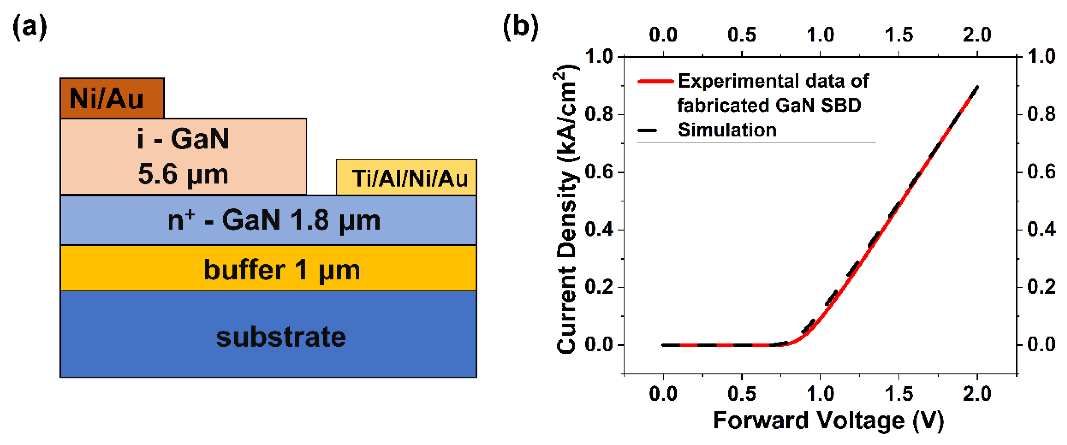
3.2.2. Forward Characteristics

The role of inter-p-GaN distance Wd and of drift layer concentration plays on the forward characteristics was also simulated and studied. Figure 6a presented the forward current density for five cases of Wd from 0 to 8 µm, while keeping Wp 1 μm wide and an i-GaN concentration of 1 × 10¹⁶/cm3. All the MPSs shared similar turn-on voltages of around 0.8 V, which was determined by the concentration of i-GaN and the work function of the metal selected. It could be found that MPSs exhibit better forward characteristics than pure P-i-N at a low bias range, typically below 5 V. As the ratio of Wd/Wp was increased, the current density was increased for voltages ranging from 0.8 to around 8 V, as a result of the higher portion of Schottky contact as a conduction channel. On the other hand, the pure P-i-N diode, which had a relatively large turn-on voltage, showed a relatively lower differential on resistance (due to conductivity modulation), meaning that the current density could overrun that of the MPS at a relatively large bias, typically over 7 V.
Figure 6c,d shows a comparison of the current density for MPSs (i-GaN concentration of 1 × 10¹⁶/cm3) with Wd–Wp = 1–1 μm and Wd–Wp = 4–1 μm at 5 V. The current was mainly concentrated in and dominated by the Schottky contact region at 5 V. The larger Wd is, the larger the portion of the device (Schottky contact part) that was activated for conduction, as well as the current density through the device. As is illustrated in Figure 4 and Table 3, the better conduction induced by larger portions of Schottky contact was achieved at the cost of a reduction of more than 100 V in the breakdown voltage.
Figure 6b shows the comparison of forward current density among MPSs with various i-GaN concentrations and physical dimensions. It could be observed that the MPSs with relatively high background concentrations tend to exhibit higher currents after turn-on, due to the higher intrinsic carrier concentration for conduction. (More results about MPSs with i-GaN concentrations of 2 × 10¹⁶/cm3 can be found in Figure S3, Supplementary Materials).

4. Conclusions

The influence of lateral physical dimensions and of drift layer background concentration was assessed and studied. The model parameters used in the simulation study were carefully calibrated with fabricated GaN SBD and GaN P-i-N diodes to ensure the parameters’ authenticity. Extending inter-p-GaN region distance Wd enhanced the forward conduction capability, especially at a low bias range. At the same time, the electrical field screening effects were compromised so that a reduced breakdown voltage was observed. When reducing the drift layer background concentration, a higher breakdown voltage is expected for each combination of Wd–Wp, as larger portions of the drift layer itself could be depleted by sustaining higher reverse voltage. However, lower drift layer concentration would also lead to a trade-off in forward conduction capabilities. The design of MPS diodes has to take both forward and reverse characteristics into account. The simulation method and results in this study provide a guideline for designing MPSs and assessing GaN MPS performance, which combines the merits of both SBD and P-i-N diodes for high-voltage and low-loss applications.

Supplementary Materials

The following are available online at https://www.mdpi.com/2079-9292/8/12/1550/s1. Figure S1: E-field distribution of SBD reported by S. Yang et al. at −900 V. Figure S2: (a,b) E-field distribution of GaN P-i-N diodes with i-GaN concentration of 2 × 10¹⁶/cm3 and 2 × 10¹⁶/cm3. Figure S3: (a) Forward characteristic of (2 × 10¹⁶/cm3) GaN MPSs with various Wd, while keeping Wp 1 μm wide. (b,c) current density distribution of MPSs with Wd–Wp = 1–1 μm and Wd–Wp = 6–1 μm at 5 V. Figure S4: (a,b) Hole concentration distribution of reverse biased GaN MPSs at 300 K and 400 K, respectively. Table 1: Extracted hole concentration distribution at different temperatures. Figure S5: (a) Forward current of fabricated GaN P-i-N diodes at four temperatures. (b) Forward current of fabricated GaN MPS diodes at 400 K and 450 K. Figure S6: (a) Reverse leakage current of GaN MPSs with 1 × 1016 cm−3 i-GaN concentration and Wd–Wp = 2–1 μm at four temperatures. Figure S7: (ad) Figure 1b, Figure 2d, Figure 6a,b in the manuscript were plotted in a log scale, simulation code of Wd–Wp = 2–1 μm GaN MPS.

Author Contributions

Conceptualization, Y.Z. and X.Z.; methodology, Y.Z. and X.Z.; validation, X.L.; formal analysis, Y.Z.; supervision, X.Z.; writing—original draft preparation, Y.Z. and X.Z.; writing—review and editing, X.Z.; funding acquisition, X.Z. All authors have read and agreed to the published version of the manuscript.

Funding

This work was supported by the ShanghaiTech University Startup Fund and sponsored by the Shanghai Pujiang Program No. 18PJ1408200 and the Shanghai Eastern Scholar (Youth) Program.

Conflicts of Interest

The authors declare no conflict of interest.

References

  1. Mishra, U.K.; Shen, L.; Kazior, T.E.; Wu, Y. GaN-Based RF Power Devices and Amplifiers. Proc. IEEE 2008, 96, 287–305. [Google Scholar] [CrossRef]
  2. Chowdhury, S.; Mishra, U.K. Lateral and Vertical Transistors Using the AlGaN/GaN Heterostructure. IEEE Trans. Electron Devices 2013, 60, 3060–3066. [Google Scholar] [CrossRef]
  3. Mohammad, S.N.; Salvador, A.A.; Morkoc, H. Emerging gallium nitride based devices. Proc. IEEE 1995, 83, 1306–1355. [Google Scholar] [CrossRef]
  4. Millán, J.; Godignon, P.; Perpiñà, X.; Pérez-Tomás, A.; Rebollo, J. A Survey of Wide Bandgap Power Semiconductor Devices. IEEE Trans. Power Electron. 2014, 29, 2155–2163. [Google Scholar] [CrossRef]
  5. Han, S.; Yang, S.; Sheng, K. High-Voltage and High-ION/IOFF Vertical GaN-on-GaN Schottky Barrier Diode With Nitridation-Based Termination. IEEE Electron Device Lett. 2018, 39, 572–575. [Google Scholar] [CrossRef]
  6. Tsou, C.; Wei, K.; Lian, Y.; Hsu, S.S.H. 2.07-kV AlGaN/GaN Schottky Barrier Diodes on Silicon With High Baliga’s Figure-of-Merit. IEEE Electron Device Lett. 2016, 37, 70–73. [Google Scholar] [CrossRef]
  7. Zhu, M.; Song, B.; Qi, M.; Hu, Z.; Nomoto, K.; Yan, X.; Cao, Y.; Johnson, W.; Kohn, E.; Jena, D.; et al. 1.9-kV AlGaN/GaN Lateral Schottky Barrier Diodes on Silicon. IEEE Electron Device Lett. 2015, 36, 375–377. [Google Scholar] [CrossRef]
  8. Zhang, Y.; Sun, M.; Piedra, D.; Azize, M.; Zhang, X.; Fujishima, T.; Palacios, T. GaN-on-Si Vertical Schottky and p-n Diodes. IEEE Electron Device Lett. 2014, 35, 618–620. [Google Scholar] [CrossRef]
  9. Wang, Y.; Li, Z.; Hao, Y.; Luo, X.; Fang, J.; Ma, Y.; Yu, C.; Cao, F. Evaluation by Simulation of AlGaN/GaN Schottky Barrier Diode (SBD) With Anode-Via Vertical Field Plate Structure. IEEE Trans. Electron Devices 2018, 65, 2552–2557. [Google Scholar] [CrossRef]
  10. Ohta, H.; Asai, N.; Mishima, T.; Horikiri, F.; Narita, Y.; Yoshida, T. Stable Fabrication of High Breakdown Voltage Mesa-Structure Vertical GaN p-n Junction Diodes Using Electrochemical Etching. In Proceedings of the IEEE International Meeting for Future of Electron Devices, Kansai (IMFEDK), Kyoto, Japan, 21–22 June 2018; pp. 1–2. [Google Scholar] [CrossRef]
  11. Yu, C.J.; Lu, J.Y.; Shan, L.W.; Chen, C.J.; Liao, J.H.; Wu, M.C. Over 1 GW/cm2 for high-power GaN p-i-n diodes with edge termination structure and laser annealing. J. Vac. Sci. Technol. B 2019, 37, 5. [Google Scholar] [CrossRef]
  12. Maeda, T.; Narita, T.; Ueda, H.; Kanechika, M.; Uesugi, T.; Kachi, T.; Kimoto, T.; Horita, M.; Suda, J. Parallel-Plane Breakdown Fields of 2.8–3.5 MV/cm in GaN-on-GaN p-n Junction Diodes with Double-Side-Depleted Shallow Bevel Termination. In Proceedings of the IEEE International Electron Devices Meeting (IEDM), San Francisco, CA, USA, 1–5 December 2018. [Google Scholar] [CrossRef]
  13. Hu, Z.Y.; Nomoto, K.; Qi, M.; Li, W.S.; Zhu, M.D.; Gao, X.; Jena, D.; Xing, H.G. 1.1-kV Vertical GaN p-n Diodes With p-GaN Regrown by Molecular Beam Epitaxy. IEEE Electron Device Lett. 2017, 38, 1071–1074. [Google Scholar] [CrossRef]
  14. Nomoto, K.; Song, B.; Hu, Z.; Zhu, M.; Qi, M.; Kaneda, N.; Mishima, T.; Nakamura, T.; Jena, D.; Xing, H.G. 1.7-kV and 0.55-mΩ·cm2 GaN p-n Diodes on Bulk GaN Substrates With Avalanche Capability. IEEE Electron Device Lett. 2016, 37, 161–164. [Google Scholar] [CrossRef]
  15. Limb, J.B.; Yoo, D.; Ryou, J.; Shen, S.; Dupuis, R.D. Low on-resistance GaN pin rectifiers grown on 6H-SiC substrates. Electron. Lett. 2007, 43, 67–68. [Google Scholar] [CrossRef]
  16. Liu, W.K.; Xu, W.Z.; Zhou, D.; Ren, F.F.; Chen, D.J.; Yu, P.; Zhang, R.; Zheng, Y.D.; Lu, H. Avalanche Ruggedness of GaN p-i-n Diodes Grown on Sapphire Substrate. Phys. Status Solidi A Appl. Mater. 2018, 215, 6. [Google Scholar] [CrossRef]
  17. Shan, L.W.; Liu, Z.Y.; Lin, M.P.; Yu, C.J.; Hsieh, K.C.; Wu, M.C. Electrical analyses of GaN PIN diodes grown on patterned sapphire substrates. J. Vac. Sci. Technol. B 2017, 35, 4. [Google Scholar] [CrossRef]
  18. Harrison, S.E.; Shao, Q.; Frye, C.D.; Voss, L.F.; Nikolić, R.J. 1.1 kV vertical p-i-n GaN-on-sapphire diodes. In Proceedings of the 76th Device Research Conference (DRC), Santa Barbara, CA, USA, 24–27 June 2018; pp. 1–2. [Google Scholar] [CrossRef]
  19. Khadar, R.A.; Liu, C.; Zhang, L.Y.; Xiang, P.; Cheng, K.; Matioli, E. 820-V GaN-on-Si Quasi-Vertical p-i-n Diodes With BFOM of 2.0 GW/cm(2). IEEE Electron Device Lett. 2018, 39, 401–404. [Google Scholar] [CrossRef] [Green Version]
  20. Zou, X.; Zhang, X.; Lu, X.; Tang, C.W.; Lau, K.M. Fully Vertical GaN p-i-n Diodes Using GaN-on-Si Epilayers. IEEE Electron Device Lett. 2016, 37, 636–639. [Google Scholar] [CrossRef]
  21. Mase, S.; Hamada, T.; Freedsman, J.J.; Egawa, T. Effect of Drift Layer on the Breakdown Voltage of Fully-Vertical GaN-on-Si p-n Diodes. IEEE Electron Device Lett. 2017, 38, 1720–1723. [Google Scholar] [CrossRef]
  22. Mase, S.; Urayama, Y.; Hamada, T.; Freedsman, J.J.; Egawa, T. Novel fully vertical GaN p-n diode on Si substrate grown by metalorganic chemical vapor deposition. Appl. Phys. Express 2016, 9, 4. [Google Scholar] [CrossRef]
  23. Ohta, H.; Kaneda, N.; Horikiri, F.; Narita, Y.; Yoshida, T.; Mishima, T.; Nakamura, T. Vertical GaN p-n Junction Diodes With High Breakdown Voltages Over 4 kV. IEEE Electron Device Lett. 2015, 36, 1180–1182. [Google Scholar] [CrossRef]
  24. Zhang, X.; Zou, X.; Lu, X.; Tang, C.W.; Lau, K.M. Fully- and Quasi-Vertical GaN-on-Si p-i-n Diodes: High Performance and Comprehensive Comparison. IEEE Trans. Electron Devices 2017, 64, 809–815. [Google Scholar] [CrossRef]
  25. Pribytny, P.; Donoval, D.; Chvala, A.; Marek, J.; Molnar, M. Electro-thermal analysis and optimization of edge termination of power diode supported by 2D numerical modeling and simulation. Microelectron. Reliab. 2012, 52, 463–468. [Google Scholar] [CrossRef]
  26. Feng, G.; Suda, J.; Kimoto, T. Space-Modulated Junction Termination Extension for Ultrahigh-Voltage p-i-n Diodes in 4H-SiC. IEEE Trans. Electron Devices 2012, 59, 414–418. [Google Scholar] [CrossRef]
  27. Slobodyan, O.; Smith, T.; Flicker, J.; Sandoval, S.; Matthews, C.; van Heukelom, M.; Kaplar, R.; Atcitty, S. Hard-switching reliability studies of 1200 V vertical GaN PiN diodes. MRS Commun. 2018, 8, 1413–1417. [Google Scholar] [CrossRef]
  28. Matthews, C.; Flicker, J.; Kaplar, R.; Heukelom, M.V.; Attcity, S.; Kizilyalli, I.C.; Aktas, O. Switching characterization of vertical GaN PiN diodes. In Proceedings of the IEEE 4th Workshop on Wide Bandgap Power Devices and Applications (WiPDA), Fayetteville, AR, USA, 7–9 November 2016; pp. 135–138. [Google Scholar] [CrossRef]
  29. Baliga, B.J. Analysis of a high-voltage merged p-i-n/Schottky (MPS) rectifier. Electron Device Lett. 1987, 8, 407–409. [Google Scholar] [CrossRef]
  30. Baliga, B.J. Advanced Power Rectifier Concepts; Springer: New York, NY, USA, 2009; pp. 195–285. [Google Scholar]
  31. Baliga, B.J. Gallium Nitride and Silicon Carbide Power Devices; World Scientific: Singapore, 2017. [Google Scholar]
  32. Jiang, Y.F.; Sung, W.; Baliga, J.; Wang, S.Z.; Lee, B.; Huang, A. Electrical Characteristics of 10-kV 4H-SiC MPS Rectifiers with High Schottky Barrier Height. J. Electron. Mater. 2018, 47, 927–931. [Google Scholar] [CrossRef]
  33. Wu, J.P.; Ren, N.; Wang, H.Y.; Sheng, K. 1.2-kV 4H-SiC Merged PiN Schottky Diode With Improved Surge Current Capability. IEEE J. Emerg. Sel. Top. Power Electron. 2019, 7, 1496–1504. [Google Scholar] [CrossRef]
  34. Wu, J.; Fursin, L.; Li, Y.Z.; Alexandrov, P.; Weiner, M.; Zhao, J.H. 4.3 kV 4H-SiC merged PiN/Schottky diodes. Semicond. Sci. Technol. 2006, 21, 987–991. [Google Scholar] [CrossRef]
  35. Tone, K.; Zhao, J.H.; Weiner, M.; Pan, M. Fabrication and Testing of 1000 V–60 A 4H-SiC MPS Diodes in an Inductive Half-Bridge Circuit. In Silicon Carbide and Related Materials—1999 Pts, 1 & 2; Carter, C.H., Devaty, R.P., Rohrer, G.S., Eds.; Trans Tech Publications Ltd.: Zurich-Uetikon, Switzerland, 2000; Volume 338-3, pp. 1187–1190. [Google Scholar] [CrossRef]
  36. Palanisamy, S.; Fichther, S.; Lutz, J.; Basler, T.; Rupp, R. Various structures of 1200 V SiC MPS diode models and their simulated surge current behavior in comparison to measurement. In Proceedings of the 28th International Symposium on Power Semiconductor Devices and ICs (ISPSD), Prague, Czech Republic, 12–16 June 2016; pp. 235–238. [Google Scholar] [CrossRef]
  37. Heinze, B.; Lutz, J.; Neumeister, M.; Rupp, R.; Holz, M. Surge current ruggedness of silicon carbide Schottky- and merged-pin-Schottky diodes. In Proceedings of the20th International Symposium on Power Semiconductor Devices and IC’s, Orlando, FL, USA, 18–22 May 2008; p. 245. [Google Scholar] [CrossRef]
  38. Sawant, S.; Baliga, B.J. 4 kV merged PiN Schottky (MPS) rectifiers. In Proceedings of the10th International Symposium on Power Semiconductor Devices and ICs. ISPSD’98 (IEEE Cat. No. 98CH36212), Kyoto, Japan, 3–6 June 1998; pp. 297–300. [Google Scholar] [CrossRef]
  39. Li, W.; Nomoto, K.; Pilla, M.; Pan, M.; Gao, X.; Jena, D.; Xing, H.G. Design and Realization of GaN Trench Junction-Barrier-Schottky-Diodes. IEEE Trans. Electron Devices 2017, 64, 1635–1641. [Google Scholar] [CrossRef]
  40. Irokawa, Y.; Kim, J.; Ren, F.; Baik, K.H.; Gila, B.P.; Abernathy, C.R.; Pearton, S.J.; Pan, C.C.; Chen, G.T.; Chyi, J.I.; et al. Si+ ion implanted MPS bulk GaN diodes. Solid State Electron. 2004, 48, 827–830. [Google Scholar] [CrossRef]
  41. Hayashida, T.; Nanjo, T.; Furukawa, A.; Yamamuka, M. Vertical GaN merged PiN Schottky diode with a breakdown voltage of 2 kV. Appl. Phys. Express 2017, 10. [Google Scholar] [CrossRef]
  42. TCAD World Leader, Silvaco Inc., USA. Available online: https://www.silvaco.com.cn/tech_lib_TCAD/tech_info/devicesimulation/pdf/TCADWL_May2010.pdfA (accessed on 29 July 2019).
  43. Silvaco Data System Inc. Atlas User Manual; Santa: Clara, CA, USA, 2009. [Google Scholar]
  44. Chaudhuri, R.; Bader, S.J.; Chen, Z.; Muller, D.A.; Xing, H.G.; Jena, D. A polarization-induced 2D hole gas in undoped gallium nitride quantum wells. Science 2019, 365, 1454. [Google Scholar] [CrossRef] [PubMed] [Green Version]
  45. Sabui, G.; Parbrook, P.J.; Arredondo-Arechavala, M.; Shen, Z.J. Modeling and simulation of bulk gallium nitride power semiconductor devices. AIP Adv. 2016, 6, 14. [Google Scholar] [CrossRef]
  46. Yates, L.; Pavlidis, G.; Graham, S.; Usami, S.; Nagamatsu, K.; Honda, Y.; Amano, H. Electrical and Thermal Analysis of Vertical GaN-on-GaN PN Diodes. In Proceedings of the 17th IEEE Intersociety Conference on Thermal and Thermomechanical Phenomena in Electronic Systems (ITherm), San Diego, CA, USA, 29 May–1 June 2018; pp. 831–837. [Google Scholar] [CrossRef]
  47. Zhang, Y.H.; Piedra, D.; Sun, M.; Hennig, J.; Dadgar, A.; Yu, L.L.; Palacios, T. High-Performance 500 V Quasi- and Fully-Vertical GaN-on-Si pn Diodes. IEEE Electron Device Lett. 2017, 38, 248–251. [Google Scholar] [CrossRef]
  48. Dharmarasu, N.; Karthikeyan, G.S.; Agrawal, M.; Alex, S.T.L.; Radhakrishnan, K. AlGaN/GaN HEMT grown on SiC with carbon doped GaN buffer by MOCVD. In Proceedings of the Electron Devices Technology and Manufacturing Conference (EDTM), Singapore, 12–15 March 2019; pp. 434–436. [Google Scholar] [CrossRef]
Figure 1. (a) A schematic cross-section of fabricated GaN Schottky barrier diodes (SBDs); (b) the measured current density and simulated I-V curve using the parameters in Table 1.
Electronics 08 01550 g001
Figure 2. (a) A schematic cross-sectional view of fabricated GaN P-i-N diodes; (b) the extracted experimental data of device’s characteristics; (c) the electrical field distribution of P-i-N diodes with various drift layer thicknesses at breakdown voltage; (d) the measured P-i-N diode current densities and simulated I-V curve using the parameters in Table 1.
Electronics 08 01550 g002
Figure 3. (a) A schematic cross-sectional view of the GaN P-i-N diode with extended i-GaN thickness; (b) a schematic view of the GaN merged P-i-N Schottky (MPS) diode. Wp and Wd denote p-GaN box width and inter-p-GaN region distance, respectively.
Electronics 08 01550 g003
Figure 4. (a–c) E-field distribution of GaN MPS (i-GaN background concentration 2 × 10¹⁶/cm3) with Wd–Wp = 0.5–1 μm, Wd–Wp = 4–1 μm, and Wd–Wp = 6–1 μm at a reverse bias of 400 V.
Electronics 08 01550 g004
Figure 5. (a–c) E-field distribution of GaN MPS (i-GaN background concentration 1 × 10¹⁶/cm3) with Wd–Wp = 0.5–1 μm, Wd–Wp = 8–1 μm, and Wd–Wp = 9–1 μm at a reverse bias of 620 V.
Electronics 08 01550 g005
Figure 6. (a) The forward characteristics of GaN MPSs (i-GaN concentration of 2 × 10¹⁶/cm3) with various Wd, while keeping Wp 1 μm. (b) The comparison of forward current density among GaN MPSs. (c,d) The current density distribution of MPSs with Wd–Wp = 1–1μm and Wd–Wp = 4–1 μm at 5 V.
Electronics 08 01550 g006
Table 1. Parameters used in GaN-based device simulations and key models.
ParametersQuantityUnitDescription
Eg (300)3.42eVDirect band gap at 300 K
Affinity4.1eVAffinity
Permittivity9.5-Permittivity
Workf5.2eVWork function
Mun400/100cm2/V·sElectron mobility
Mup10cm2/V·sHole mobility
Vstan1.9 × 107cm/sElectron saturation velocity
Vstap7 × 106cm/sHole saturation velocity
Taun00.7 × 10−9sElectron lifetime
Taup02 × 10−9sHole lifetime
Nsrhn4 × 1018cm−3Shockley-Read-Hall concentration-dependent lifetime model for electrons
Nsrhp4 × 1018cm−3Shockley-Read-Hall concentration-dependent lifetime model for holes
Augn3 × 10−31cm6/sAuger recombination parameter for electrons
Augp3 × 10−31cm6/sAuger recombination parameter for holes
Table 2. The E-field at Schottky contact and the peak E-field inside the MPS (i-GaN background concentration 2 × 10¹⁶/cm3) with various combinations of Wd–Wp. The numbers underlined indicate that the E-field reached corresponding critical E-fields of breakdown.
Wd–WpApplying VoltageE-Field at Schottky Contact (MV/cm)Peak E-Field Inside MPS (MV/cm)
0.5–1 μm−550 V0.42.1
2–1 μm−430 V1.342.12
4–1 μm−400 V1.612.11
5–1 μm−370 V1.602.05
6–1 μm−355 V1.602.01
Table 3. The E-field at Schottky contact and the peak E-field inside MPS (i-GaN background concentration 1 × 10¹⁶/cm3) with various combinations of Wd–Wp. The numbers underlined indicate that the E-field reached corresponding critical E-fields of breakdown.
Wd–WpApplying VoltageE-Field at Schottky Contact (MV/cm)Peak E-Field Inside MPS (MV/cm)
0.5–1 μm−800 V0.22.11
2–1 μm−660 V1.222.1
4–1 μm−635 V1.52.1
8–1 μm−620 V1.6052.117
9–1 μm−610 V1.5972.086

